EP3086475B1 - Dispositif électronique ayant une structure de dissipation de chaleur - Google Patents
Dispositif électronique ayant une structure de dissipation de chaleur Download PDFInfo
- Publication number
- EP3086475B1 EP3086475B1 EP16166259.8A EP16166259A EP3086475B1 EP 3086475 B1 EP3086475 B1 EP 3086475B1 EP 16166259 A EP16166259 A EP 16166259A EP 3086475 B1 EP3086475 B1 EP 3086475B1
- Authority
- EP
- European Patent Office
- Prior art keywords
- electronic device
- heat dissipation
- dissipation plate
- battery pack
- disposed
- Prior art date
- Legal status (The legal status is an assumption and is not a legal conclusion. Google has not performed a legal analysis and makes no representation as to the accuracy of the status listed.)
- Active
Links
Images


Classifications
-
- H—ELECTRICITY
- H05—ELECTRIC TECHNIQUES NOT OTHERWISE PROVIDED FOR
- H05K—PRINTED CIRCUITS; CASINGS OR CONSTRUCTIONAL DETAILS OF ELECTRIC APPARATUS; MANUFACTURE OF ASSEMBLAGES OF ELECTRICAL COMPONENTS
- H05K7/00—Constructional details common to different types of electric apparatus
- H05K7/20—Modifications to facilitate cooling, ventilating, or heating
- H05K7/2039—Modifications to facilitate cooling, ventilating, or heating characterised by the heat transfer by conduction from the heat generating element to a dissipating body
-
- G—PHYSICS
- G06—COMPUTING OR CALCULATING; COUNTING
- G06F—ELECTRIC DIGITAL DATA PROCESSING
- G06F1/00—Details not covered by groups G06F3/00 - G06F13/00 and G06F21/00
- G06F1/16—Constructional details or arrangements
- G06F1/20—Cooling means
- G06F1/203—Cooling means for portable computers, e.g. for laptops
-
- G—PHYSICS
- G06—COMPUTING OR CALCULATING; COUNTING
- G06F—ELECTRIC DIGITAL DATA PROCESSING
- G06F1/00—Details not covered by groups G06F3/00 - G06F13/00 and G06F21/00
- G06F1/16—Constructional details or arrangements
- G06F1/1613—Constructional details or arrangements for portable computers
- G06F1/163—Wearable computers, e.g. on a belt
-
- G—PHYSICS
- G06—COMPUTING OR CALCULATING; COUNTING
- G06F—ELECTRIC DIGITAL DATA PROCESSING
- G06F1/00—Details not covered by groups G06F3/00 - G06F13/00 and G06F21/00
- G06F1/16—Constructional details or arrangements
- G06F1/1613—Constructional details or arrangements for portable computers
- G06F1/1633—Constructional details or arrangements of portable computers not specific to the type of enclosures covered by groups G06F1/1615 - G06F1/1626
- G06F1/1635—Details related to the integration of battery packs and other power supplies such as fuel cells or integrated AC adapter
-
- G—PHYSICS
- G06—COMPUTING OR CALCULATING; COUNTING
- G06F—ELECTRIC DIGITAL DATA PROCESSING
- G06F1/00—Details not covered by groups G06F3/00 - G06F13/00 and G06F21/00
- G06F1/16—Constructional details or arrangements
- G06F1/1613—Constructional details or arrangements for portable computers
- G06F1/1633—Constructional details or arrangements of portable computers not specific to the type of enclosures covered by groups G06F1/1615 - G06F1/1626
- G06F1/1656—Details related to functional adaptations of the enclosure, e.g. to provide protection against EMI, shock, water, or to host detachable peripherals like a mouse or removable expansions units like PCMCIA cards, or to provide access to internal components for maintenance or to removable storage supports like CDs or DVDs, or to mechanically mount accessories
-
- G—PHYSICS
- G06—COMPUTING OR CALCULATING; COUNTING
- G06F—ELECTRIC DIGITAL DATA PROCESSING
- G06F1/00—Details not covered by groups G06F3/00 - G06F13/00 and G06F21/00
- G06F1/16—Constructional details or arrangements
- G06F1/1613—Constructional details or arrangements for portable computers
- G06F1/1633—Constructional details or arrangements of portable computers not specific to the type of enclosures covered by groups G06F1/1615 - G06F1/1626
- G06F1/1675—Miscellaneous details related to the relative movement between the different enclosures or enclosure parts
- G06F1/1679—Miscellaneous details related to the relative movement between the different enclosures or enclosure parts for locking or maintaining the movable parts of the enclosure in a fixed position, e.g. latching mechanism at the edge of the display in a laptop or for the screen protective cover of a PDA
-
- G—PHYSICS
- G06—COMPUTING OR CALCULATING; COUNTING
- G06F—ELECTRIC DIGITAL DATA PROCESSING
- G06F1/00—Details not covered by groups G06F3/00 - G06F13/00 and G06F21/00
- G06F1/16—Constructional details or arrangements
- G06F1/1613—Constructional details or arrangements for portable computers
- G06F1/1633—Constructional details or arrangements of portable computers not specific to the type of enclosures covered by groups G06F1/1615 - G06F1/1626
- G06F1/1684—Constructional details or arrangements related to integrated I/O peripherals not covered by groups G06F1/1635 - G06F1/1675
- G06F1/1686—Constructional details or arrangements related to integrated I/O peripherals not covered by groups G06F1/1635 - G06F1/1675 the I/O peripheral being an integrated camera
-
- G—PHYSICS
- G06—COMPUTING OR CALCULATING; COUNTING
- G06F—ELECTRIC DIGITAL DATA PROCESSING
- G06F1/00—Details not covered by groups G06F3/00 - G06F13/00 and G06F21/00
- G06F1/16—Constructional details or arrangements
- G06F1/1613—Constructional details or arrangements for portable computers
- G06F1/1633—Constructional details or arrangements of portable computers not specific to the type of enclosures covered by groups G06F1/1615 - G06F1/1626
- G06F1/1684—Constructional details or arrangements related to integrated I/O peripherals not covered by groups G06F1/1635 - G06F1/1675
- G06F1/1688—Constructional details or arrangements related to integrated I/O peripherals not covered by groups G06F1/1635 - G06F1/1675 the I/O peripheral being integrated loudspeakers
-
- G—PHYSICS
- G06—COMPUTING OR CALCULATING; COUNTING
- G06F—ELECTRIC DIGITAL DATA PROCESSING
- G06F1/00—Details not covered by groups G06F3/00 - G06F13/00 and G06F21/00
- G06F1/16—Constructional details or arrangements
- G06F1/18—Packaging or power distribution
- G06F1/189—Power distribution
-
- H—ELECTRICITY
- H01—ELECTRIC ELEMENTS
- H01M—PROCESSES OR MEANS, e.g. BATTERIES, FOR THE DIRECT CONVERSION OF CHEMICAL ENERGY INTO ELECTRICAL ENERGY
- H01M10/00—Secondary cells; Manufacture thereof
- H01M10/60—Heating or cooling; Temperature control
- H01M10/65—Means for temperature control structurally associated with the cells
- H01M10/655—Solid structures for heat exchange or heat conduction
- H01M10/6554—Rods or plates
-
- H—ELECTRICITY
- H04—ELECTRIC COMMUNICATION TECHNIQUE
- H04B—TRANSMISSION
- H04B1/00—Details of transmission systems, not covered by a single one of groups H04B3/00 - H04B13/00; Details of transmission systems not characterised by the medium used for transmission
- H04B1/02—Transmitters
- H04B1/03—Constructional details, e.g. casings, housings
- H04B1/036—Cooling arrangements
-
- H—ELECTRICITY
- H04—ELECTRIC COMMUNICATION TECHNIQUE
- H04M—TELEPHONIC COMMUNICATION
- H04M1/00—Substation equipment, e.g. for use by subscribers
- H04M1/02—Constructional features of telephone sets
- H04M1/0202—Portable telephone sets, e.g. cordless phones, mobile phones or bar type handsets
-
- H—ELECTRICITY
- H05—ELECTRIC TECHNIQUES NOT OTHERWISE PROVIDED FOR
- H05K—PRINTED CIRCUITS; CASINGS OR CONSTRUCTIONAL DETAILS OF ELECTRIC APPARATUS; MANUFACTURE OF ASSEMBLAGES OF ELECTRICAL COMPONENTS
- H05K7/00—Constructional details common to different types of electric apparatus
- H05K7/20—Modifications to facilitate cooling, ventilating, or heating
- H05K7/2039—Modifications to facilitate cooling, ventilating, or heating characterised by the heat transfer by conduction from the heat generating element to a dissipating body
- H05K7/20436—Inner thermal coupling elements in heat dissipating housings, e.g. protrusions or depressions integrally formed in the housing
- H05K7/20445—Inner thermal coupling elements in heat dissipating housings, e.g. protrusions or depressions integrally formed in the housing the coupling element being an additional piece, e.g. thermal standoff
-
- H—ELECTRICITY
- H04—ELECTRIC COMMUNICATION TECHNIQUE
- H04M—TELEPHONIC COMMUNICATION
- H04M1/00—Substation equipment, e.g. for use by subscribers
- H04M1/02—Constructional features of telephone sets
- H04M1/0202—Portable telephone sets, e.g. cordless phones, mobile phones or bar type handsets
- H04M1/026—Details of the structure or mounting of specific components
- H04M1/0262—Details of the structure or mounting of specific components for a battery compartment
-
- Y—GENERAL TAGGING OF NEW TECHNOLOGICAL DEVELOPMENTS; GENERAL TAGGING OF CROSS-SECTIONAL TECHNOLOGIES SPANNING OVER SEVERAL SECTIONS OF THE IPC; TECHNICAL SUBJECTS COVERED BY FORMER USPC CROSS-REFERENCE ART COLLECTIONS [XRACs] AND DIGESTS
- Y02—TECHNOLOGIES OR APPLICATIONS FOR MITIGATION OR ADAPTATION AGAINST CLIMATE CHANGE
- Y02E—REDUCTION OF GREENHOUSE GAS [GHG] EMISSIONS, RELATED TO ENERGY GENERATION, TRANSMISSION OR DISTRIBUTION
- Y02E60/00—Enabling technologies; Technologies with a potential or indirect contribution to GHG emissions mitigation
- Y02E60/10—Energy storage using batteries
Definitions
- Various embodiments of the present disclosure relate to an electronic device that includes a heat dissipation structure.
- the electronic device which is being gradually slimmed, requires a structure that is capable of efficiently dissipating heat generated from internal parts.
- US 2010/072952 A1 discloses a structure to dissipate heat from an electronic apparatus.
- US 2009/310311 A1 discloses an electronic device provided with a heat dissipating metal plate.
- JP 2010146774 A discloses a battery pack which includes a heat dissipating plate.
- a separate plate type bracket may be disposed within the electronic device to include at least a portion of the electronic device.
- the bracket may have a die-casted or pressed structure.
- the bracket may have an injection-molded structure.
- Various embodiments of the present disclosure provide an electronic device that includes a heat dissipation structure that is capable of efficiently transferring and dissipating heat generated from a heat generating source within the electronic device.
- Various embodiments of the present disclosure provide an electronic device that includes a heat dissipation structure that is implemented to be capable of preventing electric shock beforehand.
- Various embodiments of the present disclosure provide an electronic device that includes a heat dissipation structure that is capable of contributing to the slimming and rigidity reinforcement of the electronic device.
- an electronic device includes: a housing that includes a metallic member; a battery pack that is disposed in the housing; a substrate that includes at least one heat generating source adjacent to the battery pack; and a heat dissipation plate that is disposed to overlap with at least a portion of the battery pack and the substrate, and is formed of a metallic material. Heat generated from the heat generating source may be dissipated to the battery pack and a peripheral structure through the heat dissipation plate.
- the heat dissipation plate and the housing include at least one fastening structure for electric isolation from the metallic member of the housing.
- FIGURES 1 through 9 discussed below, and the various embodiments used to describe the principles of the present disclosure in this patent document are by way of illustration only and should not be construed in any way to limit the scope of the disclosure. Those skilled in the art will understand that the principles of the present disclosure may be implemented in any suitably arranged wireless communication device.
- the following description, with reference to the accompanying drawings, is provided to assist in a comprehensive understanding of various embodiments of the present disclosure as defined by the claims and their equivalents. The description includes various specific details to assist in that understanding, but these details are to be regarded as merely examples. For example, those of ordinary skill in the art will recognize that various changes and modifications of the various embodiments described herein can be made without departing from the scope of the present disclosure. In addition, descriptions of well-known functions and constructions may be omitted for clarity and conciseness.
- a or B at least one of A or/and B
- one or more of A or/and B may include any and all combinations of words enumerated with it.
- “A or B,” “at least one of A and B”, and “at least one of A or B” describe (1) including A, (2) including B, or (3) including both A and B.
- first and second may modify various elements of various embodiments of the present disclosure, these terms do not limit the corresponding elements. For example, these terms do not limit an order and/or importance of the corresponding elements. These terms may be used for the purpose of distinguishing one element from another element.
- a first user device and a second user device both indicate user devices and may indicate different user devices.
- a first element may be referred to as a second element without departing from the scope of the present disclosure, and similarly, a second element may be referred to as a first element.
- first element e.g., a first element
- second element e.g., a second element
- the first element may be directly connected or coupled to the second element, or there may be an intervening element (e.g., a third element) between the first element and the second element.
- intervening element e.g., a third element
- the expression “configured to (or set to)” may be replaced with “suitable for,” “having the capacity to,” “designed to,” “adapted to,” “made to,” or “capable of' according to the situation.
- the term “configured to (or set to)” does not necessarily indicate “specifically designed to” in a hardware level. Instead, the expression “an apparatus configured to" may indicate that the apparatus is “capable of" along with other devices or parts in a certain situation.
- a processor configured to (set to) perform A, B, and C may be a dedicated processor, e.g., an embedded processor, for performing a corresponding operation, or a generic-purpose processor, e.g., a central processing unit (CPU) or an application processor (AP), capable of performing a corresponding operation by executing one or more software programs stored in a memory device.
- a dedicated processor e.g., an embedded processor
- a generic-purpose processor e.g., a central processing unit (CPU) or an application processor (AP), capable of performing a corresponding operation by executing one or more software programs stored in a memory device.
- a module or programming module may include at least one constituent element among the described constituent elements of an apparatus, or may omit some of them, or may further include additional constituent elements. Operations performed by a module, programming module, or other constituent elements may be executed in a sequential, parallel, repetitive, or heuristic manner. In addition, some of the operations may be executed in a different order or may be omitted, or other operations may be added.
- an electronic device may be a smart phone, a tablet personal computer (PC), a mobile phone, a video phone, an e-book reader, a desktop PC, a laptop PC, a netbook computer, a workstation, a server, a personal digital assistant (PDA), a portable multimedia player (PMP), a moving picture experts group phase 1 or phase 2 (MPEG-1 or MPEG-2) audio layer 3 (MP3) player, a mobile medical device, a camera, or a wearable device (e.g., a head-mounted-device (HMD), electronic glasses, electronic clothing, an electronic bracelet, an electronic necklace, an electronic appcessory, an electronic tattoo, a smart mirror, a smart watch, etc.).
- PDA personal digital assistant
- PMP portable multimedia player
- MPEG-1 or MPEG-2 moving picture experts group phase 2
- MP3 audio layer 3
- An electronic device may also be a smart home appliance, e.g., a television (TV), a digital versatile disc (DVD) player, an audio component, a refrigerator, an air conditioner, a vacuum cleaner, an oven, a microwave oven, a washing machine, an air cleaner, a set-top box, a home automation control panel, a security control panel, a TV box (e.g., Samsung HomeSync®, Apple TV®, or Google TV®), a game console (e.g., Xbox® or PlayStation®), an electronic dictionary, an electronic key, a camcorder, an electronic frame, and the like.
- TV television
- DVD digital versatile disc
- an audio component e.g., a refrigerator, an air conditioner, a vacuum cleaner, an oven, a microwave oven, a washing machine, an air cleaner, a set-top box, a home automation control panel, a security control panel, a TV box (e.g., Samsung HomeSync®, Apple TV®, or Google TV®), a game console (e.g
- An electronic device may also be medical equipment, such as a mobile medical device (e.g., a blood glucose monitoring device, a heart rate monitor, a blood pressure monitoring device, a temperature meter, etc.), a magnetic resonance angiography (MRA) machine, a magnetic resonance imaging (MRI) machine, a computed tomography (CT) scanner, an ultrasound machine, etc., a navigation device, a GPS receiver, an event data recorder (EDR), a flight data recorder (FDR), an in-vehicle infotainment device, electronic equipment for a ship (e.g., a ship navigation equipment and/or a gyrocompass), avionics equipment, security equipment, a head unit for vehicle, an industrial or home robot, an automatic teller machine (ATM), a point of sale (POS) device, or an Internet of things (IoT) device (e.g., a light bulb, various sensors, an electronic meter, a gas meter, a sprinkler, a fire alarm,
- An electronic device may also be a piece of furniture, a building/structure, an electronic board, an electronic signature receiving device, a projector, and/or various measuring instruments (e.g., a water meter, an electricity meter, a gas meter, a wave meter, and the like).
- various measuring instruments e.g., a water meter, an electricity meter, a gas meter, a wave meter, and the like.
- An electronic device may also be a combination of one or more of the above-mentioned devices. Further, it will be apparent to those skilled in the art that an electronic device is not limited to the above-mentioned examples.
- the term "user” may indicate a person who uses an electronic device or a device (e.g., an artificial intelligence electronic device) that uses the electronic device.
- An electronic device of a single radio environment can provide LTE service using circuit switched fall back (CSFB) that determines whether paging information of a circuit switched (CS) service network is received over an LTE network.
- CS circuit switched fall back
- the electronic device connects (or accesses) the CS service network (e.g., a 2nd generation (2G)/3rd generation (3G) network) and provides a voice call service.
- the 2G network can include one or more of a GSM network and a code division multiple access (CDMA) network.
- the 3G network can include one or more of a wideband-CDMA (WCDMA) network, a time division-synchronous CDMA (TD-SCDMA) network, and an evolution-data optimized (EV-DO) network.
- WCDMA wideband-CDMA
- TD-SCDMA time division-synchronous CDMA
- EV-DO evolution-data optimized
- the electronic device of the single radio environment can provide LTE service using single radio LTE (SRLTE), which determines whether the paging information is received by periodically switching every radio resource (e.g., receive antennas) to the CS service network (e.g., the 2G/3G network).
- SRLTE single radio LTE
- the electronic device Upon receiving the paging signal of the CS service network, the electronic device provides the voice call service by connecting the CS service network (e.g., the 2G/3G network).
- the electronic device of the single radio environment can provide LTE service using single radio dual system (SRDS), which determines whether the paging information is received by periodically switching some of radio resources (e.g., receive antennas) to the CS service network (e.g., the 2G/3G network).
- SRDS single radio dual system
- the electronic device Upon receiving the paging signal of the CS service network, the electronic device provides the voice call service by connecting the CS service network (e.g., the 2G/3G network).
- FIG. 1 illustrates a network environment including an electronic device according to an embodiment of the present disclosure.
- an electronic device 101 includes a bus 110, a processor 120, a memory 130, an input/output interface 150, a display 160, and a communication interface 170.
- the electronic device 100 can omit at least one of the components and/or include an additional component.
- the bus 110 includes a circuit for connecting the components (e.g., the processor 120, the memory 130, the input/output interface 150, the display 160, and the communication interface 170) and delivering communications (e.g., a control message) therebetween.
- the components e.g., the processor 120, the memory 130, the input/output interface 150, the display 160, and the communication interface 170
- communications e.g., a control message
- the processor 120 includes one or more of a CPU, an AP, and a communication processor (CP).
- the processor 120 processes an operation or data for control of and/or communication with another component of the electronic device 101.
- the processor 120 determines whether a call is connected over the CS service network using caller identification information (e.g., a caller phone number) of the CS service network (e.g., the 2G/3G network). For example, the processor 120 may receive incoming call information (e.g., a CS notification message or a paging request message) of the CS service network over the LTE network (e.g., CSFB). For example, the processor 120 being connected to the LTE network may receive incoming call information (e.g., a paging request message) over the CS service network (e.g., SRLTE).
- caller identification information e.g., a caller phone number
- the processor 120 may receive incoming call information (e.g., a CS notification message or a paging request message) of the CS service network over the LTE network (e.g., CSFB).
- the processor 120 being connected to the LTE network may receive incoming call information (e.g., a
- the processor 120 may obtain caller identification information from the incoming call information.
- the processor 120 displays the caller identification information on its display 160.
- the processor 120 may determine whether to connect the call based on input information corresponding to the caller identification information displayed on the display 160. For example, when detecting input information corresponding to an incoming call rejection, through the input/output interface 150, the processor 120 may restrict the voice call connection and maintains the LTE network connection. For example, when detecting input information corresponding to an incoming call acceptance, through the input/output interface 150, the processor 120 connects the voice call by connecting to the CS service network.
- the processor 120 may obtain caller identification information from the incoming call information.
- the processor 120 may determine whether to connect the call by comparing the caller identification information with a reception control list. For example, when the caller identification information is included in a first reception control list (e.g., a blacklist), the processor 120 may restrict the voice call connection and maintains the connection to the LTE network. For example, when the caller identification information is not included in the first reception control list (e.g., the blacklist), the processor 120 may connect the voice call by connecting to the CS service network. For example, when the caller identification information is included in a second reception control list (e.g., a white list), the processor 120 connects the voice call by connecting to the CS service network.
- a reception control list e.g., a blacklist
- the processor 120 may connect the voice call by connecting to the CS service network.
- the processor 120 may transmit an incoming call response message (e.g., a paging response message) to the CS service network.
- the processor 120 may suspend the LTE service and receives the caller identification information (e.g., a CS call (CC) setup message) from the CS service network.
- the processor 120 may determine whether to connect the call by comparing the caller identification information with the reception control list. For example, when the caller identification information is included in the first reception control list (e.g., the blacklist), the processor 120 may restrict the voice call connection and resumes the LTE network connection.
- the first reception control list e.g., the blacklist
- the processor 120 may connect the voice call by connecting to the CS service network.
- the processor 120 connects the voice call by connecting to the CS service network.
- the memory 130 may include volatile and/or nonvolatile memory.
- the memory 130 may store commands or data (e.g., the reception control list) relating to at least another component of the electronic device 101.
- the memory 130 stores software and/or a program 140.
- the program 140 includes a kernel 141, middleware 143, an application programming interface (API) 145, and applications 147. At least some of the kernel 141, the middleware 143, and the API 145 may be referred to as an operating system (OS).
- OS operating system
- the kernel 141 may control or manage system resources (e.g., the bus 110, the processor 120, or the memory 130) used for performing an operation or function implemented by the other programs (e.g., the middleware 143, the API 145, or the applications 147). Further, the kernel 141 provides an interface through which the middleware 143, the API 145, or the applications 147 may connect the individual elements of the electronic device 101 to control or manage the system resources.
- system resources e.g., the bus 110, the processor 120, or the memory 130
- the kernel 141 provides an interface through which the middleware 143, the API 145, or the applications 147 may connect the individual elements of the electronic device 101 to control or manage the system resources.
- the middleware 143 may function as an intermediary for the API 145 or the applications 147 to communicate with the kernel 141 and exchange data.
- the middleware 143 may process one or more task requests received from the applications 147 according to priorities thereof.
- the middleware 143 may assign priorities for using the system resources (e.g., the bus 110, the processor 120, the memory 130, and the like) of the electronic device 101, to at least one of the applications 147.
- the middleware 143 may perform scheduling or load balancing on the one or more task requests by processing the one or more task requests according to the priorities assigned thereto.
- the API 145 is an interface through which the applications 147 control functions provided from the kernel 141 or the middleware 143, and may include at least one interface or function (e.g., an instruction) for file control, window control, image processing, text control, etc.
- interface or function e.g., an instruction
- the input/output interface 150 transfers instructions or data input from a user or another external device to the other element(s) of the electronic device 101. Further, the input/output interface 150 outputs the instructions or data received from the other element(s) of the electronic device 101 to the user, a first external electronic device 102, a second external electronic device 104, or a server 106.
- the display 160 may include a liquid crystal display (LCD), a light emitting diode (LED) display, an organic LED (OLED) display, a micro electro mechanical system (MEMS) display, an electronic paper display, etc.
- the display 160 displays various types of content (e.g., a text, images, videos, icons, symbols, webpages, etc.) for the user.
- the display 160 may include a touch screen that receives a touch input, a gesture input, a proximity input, a hovering input, etc., from an electronic pen or the user's body part.
- the communication interface 170 establishes communication between the electronic device 101 and the first external electronic device 102, the second external electronic device 104, or the server 106.
- the communication interface 170 can communicate with the first external electronic device 102 through a wireless communication or a wired communication 164, and communicate with the second external electronic device 104 or the server 106 in connection to a network 162 through wireless communication or wired communication.
- the wireless communication may conform to a cellular communication protocol including at least one of LTE, LTE-advanced (LTE-A), CDMA, Wideband CDMA (WCDMA), universal mobile telecommunications system (UMTS), wireless broadband (WiBro), and GSM.
- the wired communication 164 can include at least one of universal serial bus (USB), high definition multimedia interface (HDMI), recommended standard 232 (RS-232), and plain old telephone service (POTS).
- USB universal serial bus
- HDMI high definition multimedia interface
- RS-232 recommended standard 232
- POTS plain old telephone service
- the network 162 may include a telecommunications networks, a computer network (e.g., a local area network (LAN) or a wide area network (WAN)), the Internet, a telephone network, etc.
- a computer network e.g., a local area network (LAN) or a wide area network (WAN)
- the electronic device 101 provides the LTE service in the single radio environment by use of at least one module functionally or physically separated from the processor 120.
- a display that includes a bent or curved area and is applied to a housing of an electronic device 101, in which a non-metal member and a metal member (e.g., a metal bezel) are formed through dual injection molding, but are not limited thereto.
- the display 160 may be applied to a housing, in which a metal member or a non-metal member is formed of a single material.
- Each of the first external electronic device 102 and the second external electronic device 104 may be a same or a different type of device as the electronic device 101.
- the server 106 may include a group of one or more servers.
- All or some of the operations to be executed by the electronic device 101 may be executed by the first external electronic device 102, the second external electronic device 104, and/or the server 106.
- the electronic device 101 may request some functions that are associated therewith from the first external electronic device 102, the second external electronic device 104, and/or the server 106, instead of or in addition to executing the function or service by itself.
- the first external electronic device 102, the second external electronic device 104, or the server 106 may execute the requested functions or additional functions, and may transmit the results to the electronic device 101.
- the electronic device 101 may provide the requested functions or services by processing the received results as they are or after additionally.
- a cloud computing technique, a distributed computing technique, or a client-server computing technique may be used.
- FIG. 2A is a perspective view illustrating a front side of the electronic device 200 according to various embodiments of the present disclosure.
- FIG. 2B is a perspective view illustrating a rear side of the electronic device 200 according to various embodiments of the present disclosure.
- a display 201 may be provided on the front face 2001 of the electronic device 200.
- a receiver 202 may be disposed above the display 201 so as to receive a voice of a counterpart.
- a microphone device 203 may be disposed below the display 201 so as to transmit a voice of the user of the electronic device 200.
- components for conducting various functions of the electronic device 200 may be disposed around the receiver 202 that is provided on the electronic device 200.
- the components may include at least one sensor module 204.
- the sensor module 204 may include at least one of, for example, an illuminance sensor (e.g., an optical sensor), a proximity sensor (e.g., an optical sensor), an infrared sensor, and an ultrasonic sensor.
- the components may include a front camera device 205.
- the components may include an indicator 206 that informs the user of the status information of the electronic device 200.
- the electronic device 200 may include a metal bezel 220 as a metal housing.
- the metal bezel 220 may be disposed along the rim of the electronic device 200, or may be disposed on the rim to expand to at least a portion of the rear face 2002 of the electronic device 200 that extends from the rim.
- the metal bezel 220 defines at least a portion of the thickness of the electronic device 200 along the rim of the electronic device 200, and may be formed in a closed loop shape. Without being limited thereto, however, the metal bezel 220 may be formed to serve as at least a portion of the thickness of the electronic device 200.
- the metal bezel 220 may be formed on only a portion of the rim of the electronic device 200. According to one embodiment, when the metal bezel 220 serves as a portion of the housing of the electronic device 200, the remaining portion of the housing may be replaced by a non-metallic member. In such a case, the housing may be formed by insert injection molding the non-metallic member on the metal bezel 220. According to one embodiment, the metal bezel 220 may include one or more split portions 225 and 226 such that a unit bezel section, which is separated by the split portions 225 and 226, may be used as an antenna radiator.
- an upper bezel section 223 may serve as a unit bezel section by a pair of split portions 225 that are formed at a predetermined interval.
- a lower bezel section 224 may serve as a unit bezel section by a pair of split portions 226 that are formed at a predetermined interval.
- the split portions 225 and 226 may be formed in unison when the non-metallic member is molded on the metallic member through insert injection molding.
- the metal bezel 220 has a closed loop shape along the rim, and may be arranged to serve as the whole of the thickness of the electronic device 200. According to one embodiment, when viewed from the front side of the electronic device 200, the metal bezel 220 may include a left bezel section 221, a right bezel section 222, an upper bezel section 223, and a lower bezel section 224.
- various electronic components may be disposed on the lower bezel section 224 of the electronic device.
- a speaker device 208 may be disposed at one side of the microphone device 203.
- an interface connector port 207 may be disposed in order to perform a transmission/reception function of an external device and to receive external power to charge the electronic device 200.
- an ear jack hole 209 may be disposed at one side of the interface connector port 207.
- all the above mentioned microphone device 203, speaker device 208, the interface connector port 207, and the ear jack hole 209 may be disposed within the region of the unit bezel section that is formed by a pair of split portions 226 disposed in the lower bezel section 224.
- at least one of the above-mentioned electronic components may be disposed within a region that includes the split portion 226 or outside the unit bezel section.
- various electronic components may be disposed on the upper bezel section 223 of the electronic device 200.
- a socket device(not shown) may be disposed on the upper bezel section 223 in order to insert a card type external device into the socket device 216.
- the socket device may accommodate at least one of an intrinsic ID card (e.g., a SIM card or a UIM card) for the electronic device and a memory card for storage space expansion.
- an intrinsic ID card e.g., a SIM card or a UIM card
- at least one of the above-mentioned electronic components may be disposed within a region that includes the split portions 225 or outside the split portions.
- one or more first side key buttons 211 may be disposed on the left bezel section 221 of the metal bezel 220.
- the one or more first side key buttons 211 may be disposed in one pair to protrude on the left bezel section 221 so as to serve to perform a volume up/down function, a scroll function, or the like.
- one or more second side key buttons 212 may be disposed on the right bezel section 222 of the metal bezel 220.
- the second side key buttons 212 may serve to perform a power ON/OFF function, an electronic device wake-up/slip function, or the like.
- At least one key button 210 may be disposed in at least a portion of the lower region, except the display.
- the key button 210 may perform a home key button function.
- a fingerprint recognition sensor device may be disposed on the top surface of the home key button.
- the home key button may serve to perform a first function (e.g., home screen return function or a wake-up/slip function) by an action of physically pressing the home key button, and may serve to perform a second function (e.g., a fingerprint recognition function) by an action of swiping the top surface of the home key button.
- touch pads may be disposed on the left and right of the key button 210 to perform a touch function.
- a rear camera device 213 may be disposed on the rear face 2002 of the electronic device 200, and one or more electronic components 214 may be disposed at a side of the rear camera device 213.
- the one or more electronic components 214 may include at least one of, for example, an illuminance sensor (e.g., an optical sensor), a proximity sensor (e.g., an optical sensor), an infrared sensor, an ultrasonic sensor, a heart rate sensor, and a flash device.
- the front face 2001 including the display 201 may include a flat face portion 2011, and a left bending portion 2012 and a right bending portion 2013, which are formed on the left and right of the flat face portion 2011, respectively.
- the front face 2001 of the electronic device 200 may include a display region 201 and all of the other regions (e.g., a black matrix (BM) region) by using a single window.
- the left and right bending portions 2012 and 2013 may be formed to extend in an x-axis direction of the electronic device 200 of FIG. 2A from the flat face portion 2011.
- each of the left and right bending portions 2012 and 2013 may serve as a portion of the side faces of the electronic device 200, In such a case, the left and right bending portions 2012 and 2013 may form the side faces of the electronic device 200 together with the left and right bezel sections 221 and 222 of the metal bezel 220.
- the front face 2001 including the display 201 may include at least one of the left and right bending portions 2012 and 2013.
- the front face 2001 may be configured to include only the left bending portion 2012 along the flat face portion 2011, or to include only the right bending portion 2013 along the flat face portion 2011.
- the front face 2001 may include a flexible display module that is applied to a window that includes the bending portions 2012 and 2013 on the left and right thereof, and at least a portion below the window.
- a region including the flexible display module may serve as a display region 201.
- the window may be formed through a method of simultaneously bending the top face and the rear face thereof (hereinafter, referred to as a "3D method").
- the window may be formed through a method of forming each of the left and right portions of the top face in a curved shape and forming the rear face as a flat face (hereinafter, referred to as a "2.5D" method).
- the window may be formed of a transparent glass material (e.g., sapphire glass) or a transparent synthetic resin material.
- the electronic device 200 may control the display module to selectively display information. According to one embodiment, the electronic device 200 may control the display module to configure a screen only on the flat face portion 2011. According to one embodiment, the electronic device 200 may control the display module to configure a screen on any one of the left and right bending portions 2012 and 2013 together with the flat face portion 2011. According to one embodiment, the electronic device 200 may control the display module to configure a screen only on any one of the left and right bending portions 2012 and 2013, excluding the flat face portion 2011.
- the whole of the rear face 2002 of the electronic device 200 may be formed by a single window 215.
- the rear face 2002 may include a flat face portion 2151 that is approximately centrally formed on the central portion of the rear face 2002, and a left bending portion 2152 and a right bending portion 2153, which are formed on the left and right of the flat face portion 2151, respectively.
- the window 215 may be configured through a two-and-a-half dimension (2.5D) method, in which each of the left and right bending portions 2152 and 2153 of the outer face is formed in a curved shape, and the rear face of the window 215 is formed as a flat face.
- 2.5D two-and-a-half dimension
- the window 215 may also be formed through a three dimension (3D) method like the window that is disposed on the front face 2001.
- each of the left and right bending portions 2152 and 2153 may serve as a portion of the side faces of the electronic device 200.
- the left and right bending portions 2152 and 2153 may form the side faces of the electronic device 200 together with the left and right bezel sections 221 and 222 of the metal bezel 220.
- the rear face 2002 may include only one of the left and right bending portions 2152 and 2153.
- the rear face 2002 may be configured to include only the left bending portion 2152 along the flat face portion 2151, or to include only the right bending portion 2153 along the flat face portion 2151.
- the upper left and right corner portions and lower left and right corner portions of the front face 2001 may be formed to be simultaneously inclined in the x-axis direction, y-axis direction, and z-axis direction in FIG. 2A while the window is bent.
- the upper left and right corner portions and lower left and right corner portions of the metal bezel 220 may be formed such that the heights of the side faces thereof are gradually lowered.
- the electronic device may generate heat of a high temperature by the electronic components that are mounted within the electronic device.
- the heat may be efficiently transferred and dissipated to the battery pack by the heat dissipation plate that is disposed in order to reinforce the rigidity.
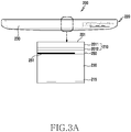
- FIG. 3A is a cross-sectional view illustrating a main portion of the electronic device 200 according to various embodiments of the present disclosure.
- the electronic device 200 may include a battery pack 230 that is disposed within a housing that includes a metal bezel 220.
- a heat dissipation plate 250 may be disposed above the battery pack 230, and a display 201 may be disposed above the heat dissipation plate 250 in a stacked method.
- the display 201 may include a window 2011 at the upper side and a display module (which may include a touch sensor) 2012 that is disposed below the window 2011.
- a rear window 215 may be further disposed below the battery pack 230. Without being limited thereto, however, the rear window 215 may be replaced by a rear cover that is integrally formed with the metal bezel 220 or an attachable/detachable battery cover.
- the heat dissipation plate 250 may be disposed such that at least a portion thereof overlaps with the battery pack 230 to be in contact with the battery pack 230. According to one embodiment, the heat dissipation plate 250 may further include an opening (a swelling gap) 251 for accommodating a swelling phenomenon that is caused by long use of the battery pack 230
- FIG. 3B illustrates a configuration of an electronic device 200 that is provided with the heat dissipation plate 250, according to various embodiments of the present disclosure.
- the heat dissipation plate 250 may be formed to have a width size that approximately corresponds to that of the electronic device 200 internally within the electronic device 200, and to have a length that is shorter than that of the electronic device 200. Without being limited thereto, however, the heat dissipation plate 250 may be formed in various sizes depending on the shape of the electronic device 200. According to one embodiment, the heat dissipation plate 250 serves as a plate that forms the internal structure in the present embodiment. However, in some cases, the plate may be assembled to an exterior housing, or to be integrated with the exterior housing so as to be seen as a single piece, or so as to form a single piece structure.
- the electronic device 200 may include a metal bezel 220 that is disposed at least along the rim of the electronic device 200, and a non-metallic member 240 may be molded, through insert injection molding, to the metal bezel 220 to be formed as a single structure with the metal bezel 220.
- the electronic device 200 may be mounted with a battery pack 230, and a printed circuit board (PCB) 231 may be disposed in parallel with the battery pack 230 to avoid the battery pack 230.
- the PCB 231 may include a main heat generating source (e.g., an AP).
- the heat dissipation plate 250 may be disposed such that it overlaps with at least a portion of each of the heat generating source of the PCB 231 and the battery pack 230. According to one embodiment, the heat dissipation plate 250 may be disposed such that it is in contact with at least a portion of the battery pack 230. According to one embodiment, the opening 251, which is formed in the heat dissipation plate 250 to handle the swelling phenomenon may be disposed in a region that generally overlaps with the central portion of the battery pack 230.
- FIG. 4A illustrates a configuration of a heat dissipation plate 250 according to various embodiments of the present disclosure.
- the heat dissipation plate 250 may be formed of a plate type metallic member. According to one embodiment, the heat dissipation plate 250 may be formed of a Cu alloy that is relatively excellent in heat conductivity.
- a Cu alloy-made heat dissipation plate 250 which is manufactured using Cu by weight of 90% or more according to an embodiment of the present disclosure, may ensure a relatively excellent heat conductivity compared to SUS304, S36(AL), or AZ91D(MG).
- the heat dissipation plate 250 may be formed to have a thickness in the range of 0.2 mm to 0.25 mm using a Cu alloy.
- external coating such as chrome (Cr) and/or painting, may be performed on the heat dissipation plate in order to improve corrosion resistance.
- various shapes may be disposed in order to improve the strength and corrosion resistance of the heat dissipation plate 250.
- various shapes of beads 252 and 253 may be formed on the heat dissipation plate 250.
- one or more beads 252 and 253 may be formed in the longitudinal direction, and may be formed in a rectangular shape.
- the longitudinal bead 252 may be disposed near the opening 251 in order to prevent the deformation of the heat dissipation plate 250 beforehand.
- the heat dissipation plate 250 may include a plurality of fasteners 254, 255, and 257 to be fixed to the metal bezel 220 of the electronic device 200, the non-metallic member (an injection-molded product) 240, or the PCB 231 by screws.
- the plurality of fasteners may include board fasteners 254 and 255 that allow the heat dissipation plate 250 to be fastened to the PCB 231, injection-molded product fasteners 257 that allow the heat dissipation plate 250 to be fastened to an injection-molded product, and locking protrusions 256 that allow the heat dissipation plate 250 to be isolated from the metal bezel 220 and fixed.
- the locking protrusions 256 may be disposed through a method of bending side faces of the heat dissipation plate 250, which is formed of a Cu alloy, and insert injection molding a non-metallic member (e.g., a PC). According to one embodiment, the locking protrusions 256 may be engaged to be locked to the inner faces of the metal bezel 220 so as to fix the heat dissipation plate 250 to the inside of the metal bezel of the electronic device 200.
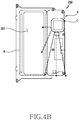
- FIG. 4B illustrates a heat dissipation structure of the heat dissipation plate 250 and an arranged state of an electronic component, according to various embodiments of the present disclosure.
- the heat dissipation plate 250 may include an "A" region, in which a battery pack 230 is disposed, and a "B" region that is a region corresponding to the PCB 231 at one side of the "A” region.
- the "B” region may include a "C” region, which is a main heat generating region corresponding to a heat generating source that is mounted on the PCB 231. Accordingly, heat generated from the heat generating source of the PCB 231 may be transferred from the "C" region to the "B” region, dissipated to the "A” region, and then dissipated to the battery pack 230, thereby configuring an efficient heat generating structure.
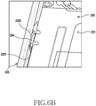
- FIG. 5 illustrates a structure that allows a heat dissipation plate 250, according to various embodiments of the present disclosure, to be fastened to an electronic device 200.
- the heat dissipation plate 250 may be fixed within the electronic device 200.
- the locking protrusions 256 of the heat dissipation plate 250 may be fixed by being locked to the side faces 2201 (see FIG. 6B ) of the metal bezel 220 by hooks 2561.
- the injection-molded product fasteners 257 of the heat dissipation plate 250 may be directly fastened to the heat dissipation plate 250 of the metallic material by screws.
- the PCB fasteners 254 and 255 of the heat dissipation plate 250 may be fixed by screws to be spaced apart from the metal bezel 220 by PEM® nuts 260.
- the PEM nuts 260 may be disposed between the PCB 231 and the metal bezel 220 so as to cause the metal bezel 220 and the PCB 231 to be spaced apart from each other.
- the PEM nuts 260 may be processed to be spaced apart from the metal bezel 220 to be insulated from the metal bezel 220.
- an insulation function may be performed by diversifying the materials, positions, and structures of the PEM nuts.
- washers 270 may also be disposed between the PCB 231 and the heat dissipation plate 250 to be used for insulation and height correction of the heat dissipation plate 250.
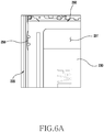
- FIGS. 6A to 6C illustrate a side mounting structure of a heat dissipation plate 250, according to various embodiments of the present disclosure.
- the heat dissipation plate 250 may include a locking protrusion 256 that is molded, through insert injection molding using a non-metallic member, in a region that is formed by being bent along the rim of the heat dissipation plate 250.
- the locking protrusion 256 may include a hook 2561 in the outward direction.
- the locking protrusion 256 may be disposed in the manner of insert injection molding a non-metallic member of a PC material in an opening that is formed in a vertically bent region in the rim of the heat dissipation plate 250.
- a locking recess 2202 to which the locking protrusion 256 is capable of being locked, may be formed at a corresponding position on the internal face 2201 of the metal bezel 220. Accordingly, merely with the operation of mounting the heat dissipation plate 250 in a direction indicated by an arrow in FIG. 6C , the locking protrusion 256 of the heat dissipation plate 250 may be coupled to the locking recess 2202 of the metal bezel 220 as a snap fit structure. According to one embodiment, such a coupling structure may contribute to maintaining the assembled state of the heat dissipation plate 250 without being moved before the heat dissipation plate 250 is fastened by screws to fastening portions.
- the heat dissipation plate 250 may be disposed in such a manner of being at least partially in contact with the PCB 231, the state in which the metal bezel 220 and the side face of the heat dissipation plate 250 are spaced apart from each other is maintained by the locking protrusion 256 of the non-metallic material (insulating material). Therefore, it is possible to prevent an electric shock accident that may be caused when the power applied to the PCB 231 is applied to the metal bezel 220.
- FIGS. 7A and 7B illustrate a screw fastening structure of a heat dissipation plate 250, according to various embodiments of the present disclosure.
- a PEM nut fixing portion 2203 may be formed on the bottom surface of the metal bezel 220.
- a PEM nut 260 may be fixed to the PEM nut fixing portion 2203 such that the PEM nut 260 protrudes to a predetermined height from the bottom surface of the metal bezel 220.
- the bottom side of the PEM nut 260 may be subjected to an insulating treatment in order to electrically insulate the PEM nut 260 from the metal bezel 220.
- a PCB 231 may be stacked on the upper portion of the PEM nut 260. According to one embodiment, since the PCB 231 may be supported by the PEM nut 260 that protrudes to a predetermined height from the bottom surface of the metal bezel 220, the PCB 231 may be practically installed to be spaced apart from the metal bezel 220 by the thickness of the metal bezel 220 and the protrusion length of the PEM nut 260.
- the heat dissipation plate 250 may be stacked on the top of the PCB 231.
- a PCB fastener 255 of the heat dissipation plate 250 may be located at a position that corresponds to the PEM nut 260. Accordingly, a screw may penetrate the PCB 231 through the PCB fastener 255 of the heat dissipation plate 250, and then may be fastened to the PEM nut 260.
- a washer 270 may be further interposed between heat dissipation plate 250 and the PCB 231.
- the washer 270 may be formed of an insulating material, and may cause the heat dissipation plate 250 and the PCB 231 to be spaced apart from each other by the height of the washer 270. With this configuration, it is possible to cut off the power, which may be applied by an FPCB of a display module stacked on the top of the heat dissipation plate 250 and may be applied to the battery pack 230 that is in contact with the heat dissipation plate 250, thereby preventing an electric shock accident beforehand.
- FIG. 8 is a cross-sectional view of a main portion, illustrating an insulation arrangement relationship of a heat dissipation plate by an enclosure that accommodates electronic components, according to various embodiments of the present disclosure.
- the insulation may be implemented by using an electronic component accommodation enclosure 280 that is essentially required in order to accommodate electronic components that are used in an existing electronic device.
- the enclosure 280 made of an insulating material may include a spacing portion 281 that extends to a side.
- the spacing portion 281 may include a through-hole 2811.
- a screw fastening portion 2204 may be formed in the bottom surface of the metal bezel 220, and the spacing portion 281 of the enclosure 280 may be disposed such that the through-hole 2811 corresponds to the screw fastening portion 2204.
- the heat dissipation plate 250 may be disposed at the upper side of the spacing portion 281 in a manner of being stacked.
- the fastener 255 of the heat dissipation plate 250, the through-hole 2811 of the spacing portion 281, and the screw fastening portion 2204 may be disposed at mutually corresponding positions, and the screw, which is inserted from the upper side of the heat dissipation plate 250, may pass through the fastener 255 and the through-hole 2811 of the spacing portion 281, and then may be fastened to the screw fastening portion 2204 of the metal bezel 220.
- the screw may be formed of an insulating material, or an insulating member may be applied to the outer surface of the screw.
- the enclosure 280 may include one or more various electronic components that are included in the electronic device.
- the electronic components may include at least one of a speaker device, a microphone device, an interface connector port, a vibration motor, a socket device, a key button assembly, various sensor modules, and a camera device.
- FIG. 9 illustrates an installation relationship of a heat dissipation structure according to various embodiments of the present disclosure.
- a housing having a mounting space may be provided.
- at least a portion of the housing may include a metallic member.
- step 903 may be performed to dispose a battery pack in the mounting space of the housing.
- a PCB may be disposed at a position adjacent to the battery pack.
- at least one heat generating source may be mounted on the PCB.
- the heat generating source may be an electronic component that is mounted on the PCB of the electronic device.
- step 907 may be performed to dispose a heat dissipation plate of a metallic material to overlap with at least a portion of the battery pack and the PCB.
- the heat dissipation plate may be disposed at a position where it overlaps with the heat generating source, and at least one bead and/or at least one perforated portion may be formed in order to prevent deformation. Accordingly, in step 909, heat generated from the heat generating source may be dissipated to the battery pack through the heat dissipation plate.
- An electronic device has an efficient heat dissipation structure while contributing to the rigidity reinforcement and slimming of the electronic device, and can prevent an electric shock accident beforehand, which may be caused by the exterior of a metallic member.
Landscapes
- Engineering & Computer Science (AREA)
- Theoretical Computer Science (AREA)
- Computer Hardware Design (AREA)
- Physics & Mathematics (AREA)
- General Engineering & Computer Science (AREA)
- Human Computer Interaction (AREA)
- General Physics & Mathematics (AREA)
- Power Engineering (AREA)
- Microelectronics & Electronic Packaging (AREA)
- Signal Processing (AREA)
- Thermal Sciences (AREA)
- Computer Networks & Wireless Communication (AREA)
- Manufacturing & Machinery (AREA)
- Chemical & Material Sciences (AREA)
- Chemical Kinetics & Catalysis (AREA)
- Electrochemistry (AREA)
- General Chemical & Material Sciences (AREA)
- Cooling Or The Like Of Electrical Apparatus (AREA)
- Casings For Electric Apparatus (AREA)
Claims (14)
- Dispositif électronique (200) comprenant :un boîtier comprenant un élément métallique (220) ;un bloc-pile (230) disposé dans le boîtier ;un substrat (231) disposé dans une position adjacente au bloc-pile, et comprenant au moins une source de génération de chaleur ; etune plaque de dissipation thermique (250) disposée de façon à chevaucher au moins une partie du bloc-pile et le substrat, et se composant d'un matériau métallique,la plaque de dissipation thermique étant configurée pour dissiper la chaleur générée par la source de génération de chaleur au bloc-pile à travers la plaque de dissipation thermique, etla plaque de dissipation thermique et le boîtier comprenant au moins une structure de fixation assurant l'isolation électrique de l'élément métallique du boîtier.
- Dispositif électronique (200) selon la revendication 1, la plaque de dissipation thermique (250) étant réalisée avec un alliage de Cu.
- Dispositif électronique (200) selon la revendication 2, la plaque de dissipation thermique (250) contenant du Cu dans la mesure de 90% en poids ou davantage.
- Dispositif électronique (200) selon la revendication 1, dans lequel, aux fins de la prévention de toute déformation, la plaque de dissipation thermique (250) comprend une formation d'une des suivantes :
au moins un cordon (252, 253), au moins une partie perforée, ou au moins un cordon et au moins une partie perforée. - Dispositif électronique (200) selon la revendication 1, dans lequel,
la plaque de dissipation thermique (250) forme au moins une partie d'un extérieur du dispositif électronique, et
une couche de revêtement est appliquée sur la plaque de dissipation thermique par au moins un des suivants : un chromage ou un procédé de peinture. - Dispositif électronique (200) selon la revendication 1, dans lequel la plaque de dissipation thermique (250) comprend une ouverture pratiquée dans une zone chevauchant le bloc-pile (230) pour recevoir un renflement du bloc-pile.
- Dispositif électronique (200) selon la revendication 6, la structure de fixation comprenant :au moins une saillie de verrouillage (256) d'une matière isolante, pratiquée dans une zone formée par cintrage le long d'un rebord de la plaque de dissipation thermique (250) ; etun évidement de verrouillage (2202) pratiqué dans un emplacement correspondant à la saillie de verrouillage sur une face interne d'un panneau métallique, etla plaque de dissipation thermique étant configurée pour être fixée sur le logement par une opération consistant à causer le verrouillage de la saillie de verrouillage dans l'évidement de verrouillage.
- Dispositif électronique (200) selon la revendication 7, la saillie de verrouillage (256) étant formée par l'insertion d'un moulage par injection en utilisant un élément non métallique d'une matière à résine synthétique sur la plaque de dissipation thermique.
- Dispositif électronique (200) selon la revendication 6, dans laquelle :la structure de fixation comprenant en outre un écrou de fixation (260) fixé sur une surface de l'élément métallique (220) du boîtier à une hauteur prédéterminée, etle substrat (231) et l'élément métallique étant isolés électriquement l'un de l'autre par l'écrou.
- Dispositif électronique (200) selon la revendication 9, une rondelle (270) possédant une hauteur prédéterminée intercalée en outre entre le substrat (231) et la plaque de dissipation thermique (250).
- Dispositif électronique (200) selon la revendication 10, une vis étant fixée sur l'écrou de fixation (260) à travers la plaque de dissipation thermique (250), la rondelle (270), et le substrat (231).
- Dispositif électronique (200) selon la revendication 10, comprenant en outre :
un module d'affichage (201) disposé au-dessus de la plaque de dissipation thermique (250), la rondelle (270) étant configurée pour couper le courant appliqué par le module d'affichage à l'élément métallique (220) à travers la plaque de dissipation thermique (250). - Dispositif électronique (200) selon la revendication 1, la structure de fixation étant configurée pour effectuer l'isolation électrique en intercalant au moins une partie d'une enceinte, contenant au moins un composant électronique placé dans le dispositif électronique, entre l'élément métallique (220) du boîtier et la plaque de dissipation thermique (250).
- Dispositif électronique (200) selon la revendication 13, les composants électroniques comprenant au moins un des suivants : un dispositif de haut-parleur (208), un dispositif de microphone (203), un orifice de connecteur d'interface (207), un moteur de vibration, un dispositif de douille (216), un ensemble de bouton-poussoir, plusieurs modules de capteurs, ou un dispositif de caméra (205).
Applications Claiming Priority (1)
| Application Number | Priority Date | Filing Date | Title |
|---|---|---|---|
| KR1020150056784A KR102376981B1 (ko) | 2015-04-22 | 2015-04-22 | 방열 구조를 갖는 전자 장치 |
Publications (2)
| Publication Number | Publication Date |
|---|---|
| EP3086475A1 EP3086475A1 (fr) | 2016-10-26 |
| EP3086475B1 true EP3086475B1 (fr) | 2019-06-19 |
Family
ID=56148060
Family Applications (1)
| Application Number | Title | Priority Date | Filing Date |
|---|---|---|---|
| EP16166259.8A Active EP3086475B1 (fr) | 2015-04-22 | 2016-04-20 | Dispositif électronique ayant une structure de dissipation de chaleur |
Country Status (4)
| Country | Link |
|---|---|
| US (1) | US9778710B2 (fr) |
| EP (1) | EP3086475B1 (fr) |
| KR (1) | KR102376981B1 (fr) |
| CN (1) | CN106068071B (fr) |
Families Citing this family (15)
| Publication number | Priority date | Publication date | Assignee | Title |
|---|---|---|---|---|
| USD801297S1 (en) * | 2016-11-11 | 2017-10-31 | Samsung Electronics Co., Ltd. | Mobile phone |
| KR20190077343A (ko) | 2016-11-22 | 2019-07-03 | 엘지전자 주식회사 | 이동 단말기 |
| USD820800S1 (en) * | 2016-11-25 | 2018-06-19 | Samsung Electronics Co., Ltd. | Mobile phone |
| USD801322S1 (en) * | 2016-11-25 | 2017-10-31 | Samsung Electronics Co., Ltd. | Mobile phone |
| CN106782090A (zh) * | 2016-12-12 | 2017-05-31 | 深圳市海诚光电有限公司 | 一种曲面显示器结构及加工工艺 |
| KR102588423B1 (ko) * | 2016-12-22 | 2023-10-12 | 삼성전자주식회사 | 벤디드 디스플레이를 통한 부품 실장 구조를 갖는 전자 장치 |
| KR102709687B1 (ko) * | 2017-01-06 | 2024-09-26 | 삼성전자주식회사 | 방열 구조 및 그를 포함하는 전자 장치 |
| KR102384532B1 (ko) * | 2017-03-15 | 2022-04-08 | 삼성전자주식회사 | 카메라 방열 구조를 가지는 전자 장치 |
| KR102469449B1 (ko) | 2018-02-09 | 2022-11-22 | 삼성전자주식회사 | 방열 구조 및 이를 포함하는 전자 장치 |
| KR102096083B1 (ko) * | 2018-04-18 | 2020-04-01 | (주)이엘테크 | 보강판 패널 및 이의 제조 방법 |
| CN209183612U (zh) * | 2018-12-29 | 2019-07-30 | 宁德时代新能源科技股份有限公司 | 电池箱 |
| KR102716243B1 (ko) | 2019-02-19 | 2024-10-11 | 삼성전자주식회사 | 열전달 부재 및 이를 포함하는 전자 장치 |
| KR102921317B1 (ko) | 2020-12-24 | 2026-02-04 | 삼성전자주식회사 | 반도체 패키지 |
| CN113999621B (zh) * | 2021-10-29 | 2023-06-23 | 维沃移动通信有限公司 | 散热膜和电子设备 |
| EP4336277A4 (fr) * | 2022-07-19 | 2024-11-13 | Samsung Electronics Co., Ltd. | Dispositif électronique comprenant un boîtier de moteur |
Family Cites Families (38)
| Publication number | Priority date | Publication date | Assignee | Title |
|---|---|---|---|---|
| JP2001284843A (ja) * | 2000-04-04 | 2001-10-12 | Furukawa Electric Co Ltd:The | 電子部品装着基板の金属筐体 |
| KR100652621B1 (ko) * | 2003-11-21 | 2006-12-06 | 엘지전자 주식회사 | 휴대용 단말기의 방열장치 |
| TWI283806B (en) * | 2005-06-07 | 2007-07-11 | Htc Corp | Portable electronic device |
| JP2007300222A (ja) * | 2006-04-27 | 2007-11-15 | Kyocera Corp | 電子機器 |
| WO2007125718A1 (fr) | 2006-04-27 | 2007-11-08 | Kyocera Corporation | Dispositif électronique |
| JP5179746B2 (ja) * | 2006-11-22 | 2013-04-10 | 京セラ株式会社 | 携帯端末装置 |
| US7957123B2 (en) * | 2007-01-30 | 2011-06-07 | Kyocera Corporation | Portable electronic device |
| KR101390082B1 (ko) | 2007-08-01 | 2014-05-28 | 삼성전자주식회사 | 프로젝터를 구비하는 이동통신 단말기 |
| WO2009057496A1 (fr) * | 2007-10-29 | 2009-05-07 | Kyocera Corporation | Dispositif terminal portable |
| KR101063028B1 (ko) * | 2008-04-23 | 2011-09-07 | 한 상 이 | 슬라이드식 개폐장치 및 슬라이드 개폐식 휴대형 전자기기 |
| JP2010146774A (ja) | 2008-12-16 | 2010-07-01 | Sanyo Electric Co Ltd | 電池パック |
| US8477499B2 (en) * | 2009-06-05 | 2013-07-02 | Laird Technologies, Inc. | Assemblies and methods for dissipating heat from handheld electronic devices |
| CA2731762A1 (fr) * | 2010-02-15 | 2011-08-15 | Research In Motion Limited | Dispositif electronique portatif a affichage tactile |
| EP2367338B1 (fr) * | 2010-02-15 | 2014-03-26 | BlackBerry Limited | Dispositif électronique incluant une plaque frontale pour fixer le dispositif |
| US8520373B2 (en) * | 2010-04-23 | 2013-08-27 | Psion Inc. | Display assembly for a portable module |
| KR101629262B1 (ko) * | 2010-05-31 | 2016-06-10 | 엘지전자 주식회사 | 이동 단말기 |
| KR101691104B1 (ko) * | 2010-07-27 | 2016-12-30 | 엘지전자 주식회사 | 이동 단말기 |
| CN103221896B (zh) * | 2010-08-19 | 2017-06-09 | 苹果公司 | 便携式电子设备 |
| US8687351B2 (en) * | 2011-03-31 | 2014-04-01 | Patientsafe Solutions, Inc. | Scanning jacket for a handheld device |
| CN102819300A (zh) * | 2011-06-08 | 2012-12-12 | 技嘉科技股份有限公司 | 散热装置及电子装置构造 |
| KR200471325Y1 (ko) * | 2011-07-13 | 2014-02-19 | 모토로라 모빌리티 엘엘씨 | 강화된 공차 누적기를 구비하는 모바일 전자 장치 |
| JP5703449B2 (ja) * | 2011-07-15 | 2015-04-22 | パナソニックIpマネジメント株式会社 | 携帯端末 |
| KR101886752B1 (ko) * | 2011-07-25 | 2018-08-08 | 엘지전자 주식회사 | 이동 단말기 |
| KR101395358B1 (ko) * | 2011-09-02 | 2014-05-14 | 주식회사 팬택 | 방수시트가 설치되는 이동통신 단말기 및 그 제조방법 |
| KR20130035879A (ko) * | 2011-09-30 | 2013-04-09 | 삼성전자주식회사 | 무선 충전 모듈을 구비하는 휴대용 단말기 |
| US9001507B2 (en) * | 2012-01-17 | 2015-04-07 | Lg Electronics Inc. | Mobile terminal |
| KR101917683B1 (ko) * | 2012-02-21 | 2018-11-13 | 엘지전자 주식회사 | 휴대 전자기기 |
| KR101861278B1 (ko) * | 2012-03-22 | 2018-05-25 | 엘지전자 주식회사 | 이동 단말기 |
| KR101977080B1 (ko) * | 2012-08-23 | 2019-05-10 | 엘지전자 주식회사 | 이동 단말기 및 이동 단말기의 케이스 제조 방법 |
| KR20140068411A (ko) * | 2012-11-28 | 2014-06-09 | 삼성전자주식회사 | 하우징, 그 가공 방법 및 이를 이용하는 전자 장치 |
| US9465414B2 (en) * | 2012-11-28 | 2016-10-11 | Nokia Corporation | User-removable device cover |
| US20140187295A1 (en) * | 2013-01-03 | 2014-07-03 | Mukesh Kumar | Electronic Device Case Capable of Performing Multiple Functions |
| KR102049791B1 (ko) * | 2013-01-08 | 2019-11-29 | 삼성전자 주식회사 | 스피커 장치를 구비하는 단말장치 및 이의 제조방법 |
| US20140233181A1 (en) * | 2013-02-21 | 2014-08-21 | Donn K. Harms | Protective Case Device with Interchangeable Faceplate System |
| US20140239781A1 (en) * | 2013-02-25 | 2014-08-28 | Motorola Mobility Llc | Electronic Device Having a Display and Method of Manufacture |
| KR101542411B1 (ko) * | 2013-04-17 | 2015-08-12 | 엘지전자 주식회사 | 이동단말기 |
| CN104640414A (zh) * | 2013-11-11 | 2015-05-20 | 富泰华精密电子(郑州)有限公司 | 移动终端 |
| JP5665948B1 (ja) * | 2013-11-14 | 2015-02-04 | 株式会社フジクラ | 携帯型電子機器の冷却構造 |
-
2015
- 2015-04-22 KR KR1020150056784A patent/KR102376981B1/ko active Active
-
2016
- 2016-04-01 US US15/089,414 patent/US9778710B2/en active Active
- 2016-04-20 EP EP16166259.8A patent/EP3086475B1/fr active Active
- 2016-04-20 CN CN201610248174.9A patent/CN106068071B/zh active Active
Non-Patent Citations (1)
| Title |
|---|
| None * |
Also Published As
| Publication number | Publication date |
|---|---|
| EP3086475A1 (fr) | 2016-10-26 |
| KR20160125804A (ko) | 2016-11-01 |
| CN106068071A (zh) | 2016-11-02 |
| US9778710B2 (en) | 2017-10-03 |
| CN106068071B (zh) | 2019-12-24 |
| US20160313773A1 (en) | 2016-10-27 |
| KR102376981B1 (ko) | 2022-03-21 |
Similar Documents
| Publication | Publication Date | Title |
|---|---|---|
| EP3086475B1 (fr) | Dispositif électronique ayant une structure de dissipation de chaleur | |
| US11611141B2 (en) | Housing, manufacturing method thereof, and electronic device having the housing | |
| US10051096B2 (en) | Battery pack mounting structure and electronic device having the same | |
| US11575779B2 (en) | Electronic device including display with bent area | |
| AU2019204571B2 (en) | Electronic device including display with bent area | |
| EP3082191B1 (fr) | Dispositif d'antenne et dispositif électronique l'incluant | |
| US20170171960A1 (en) | Board anchoring device and electronic device including the same | |
| US10206299B2 (en) | Electric connection device and electronic device having the same | |
| US10461400B2 (en) | Housing including antenna, manufacturing method of housing, and electronic device having housing | |
| US20170207808A1 (en) | Tray device and electronic device having the same |
Legal Events
| Date | Code | Title | Description |
|---|---|---|---|
| PUAI | Public reference made under article 153(3) epc to a published international application that has entered the european phase |
Free format text: ORIGINAL CODE: 0009012 |
|
| AK | Designated contracting states |
Kind code of ref document: A1 Designated state(s): AL AT BE BG CH CY CZ DE DK EE ES FI FR GB GR HR HU IE IS IT LI LT LU LV MC MK MT NL NO PL PT RO RS SE SI SK SM TR |
|
| AX | Request for extension of the european patent |
Extension state: BA ME |
|
| STAA | Information on the status of an ep patent application or granted ep patent |
Free format text: STATUS: REQUEST FOR EXAMINATION WAS MADE |
|
| 17P | Request for examination filed |
Effective date: 20170124 |
|
| RBV | Designated contracting states (corrected) |
Designated state(s): AL AT BE BG CH CY CZ DE DK EE ES FI FR GB GR HR HU IE IS IT LI LT LU LV MC MK MT NL NO PL PT RO RS SE SI SK SM TR |
|
| GRAP | Despatch of communication of intention to grant a patent |
Free format text: ORIGINAL CODE: EPIDOSNIGR1 |
|
| STAA | Information on the status of an ep patent application or granted ep patent |
Free format text: STATUS: GRANT OF PATENT IS INTENDED |
|
| INTG | Intention to grant announced |
Effective date: 20190201 |
|
| GRAS | Grant fee paid |
Free format text: ORIGINAL CODE: EPIDOSNIGR3 |
|
| GRAA | (expected) grant |
Free format text: ORIGINAL CODE: 0009210 |
|
| STAA | Information on the status of an ep patent application or granted ep patent |
Free format text: STATUS: THE PATENT HAS BEEN GRANTED |
|
| AK | Designated contracting states |
Kind code of ref document: B1 Designated state(s): AL AT BE BG CH CY CZ DE DK EE ES FI FR GB GR HR HU IE IS IT LI LT LU LV MC MK MT NL NO PL PT RO RS SE SI SK SM TR |
|
| REG | Reference to a national code |
Ref country code: GB Ref legal event code: FG4D |
|
| REG | Reference to a national code |
Ref country code: CH Ref legal event code: EP |
|
| REG | Reference to a national code |
Ref country code: IE Ref legal event code: FG4D |
|
| REG | Reference to a national code |
Ref country code: AT Ref legal event code: REF Ref document number: 1146791 Country of ref document: AT Kind code of ref document: T Effective date: 20190715 |
|
| REG | Reference to a national code |
Ref country code: DE Ref legal event code: R096 Ref document number: 602016015395 Country of ref document: DE |
|
| REG | Reference to a national code |
Ref country code: NL Ref legal event code: FP |
|
| PG25 | Lapsed in a contracting state [announced via postgrant information from national office to epo] |
Ref country code: SE Free format text: LAPSE BECAUSE OF FAILURE TO SUBMIT A TRANSLATION OF THE DESCRIPTION OR TO PAY THE FEE WITHIN THE PRESCRIBED TIME-LIMIT Effective date: 20190619 Ref country code: AL Free format text: LAPSE BECAUSE OF FAILURE TO SUBMIT A TRANSLATION OF THE DESCRIPTION OR TO PAY THE FEE WITHIN THE PRESCRIBED TIME-LIMIT Effective date: 20190619 Ref country code: FI Free format text: LAPSE BECAUSE OF FAILURE TO SUBMIT A TRANSLATION OF THE DESCRIPTION OR TO PAY THE FEE WITHIN THE PRESCRIBED TIME-LIMIT Effective date: 20190619 Ref country code: NO Free format text: LAPSE BECAUSE OF FAILURE TO SUBMIT A TRANSLATION OF THE DESCRIPTION OR TO PAY THE FEE WITHIN THE PRESCRIBED TIME-LIMIT Effective date: 20190919 Ref country code: LT Free format text: LAPSE BECAUSE OF FAILURE TO SUBMIT A TRANSLATION OF THE DESCRIPTION OR TO PAY THE FEE WITHIN THE PRESCRIBED TIME-LIMIT Effective date: 20190619 Ref country code: HR Free format text: LAPSE BECAUSE OF FAILURE TO SUBMIT A TRANSLATION OF THE DESCRIPTION OR TO PAY THE FEE WITHIN THE PRESCRIBED TIME-LIMIT Effective date: 20190619 |
|
| REG | Reference to a national code |
Ref country code: LT Ref legal event code: MG4D |
|
| PG25 | Lapsed in a contracting state [announced via postgrant information from national office to epo] |
Ref country code: BG Free format text: LAPSE BECAUSE OF FAILURE TO SUBMIT A TRANSLATION OF THE DESCRIPTION OR TO PAY THE FEE WITHIN THE PRESCRIBED TIME-LIMIT Effective date: 20190919 Ref country code: GR Free format text: LAPSE BECAUSE OF FAILURE TO SUBMIT A TRANSLATION OF THE DESCRIPTION OR TO PAY THE FEE WITHIN THE PRESCRIBED TIME-LIMIT Effective date: 20190920 Ref country code: LV Free format text: LAPSE BECAUSE OF FAILURE TO SUBMIT A TRANSLATION OF THE DESCRIPTION OR TO PAY THE FEE WITHIN THE PRESCRIBED TIME-LIMIT Effective date: 20190619 Ref country code: RS Free format text: LAPSE BECAUSE OF FAILURE TO SUBMIT A TRANSLATION OF THE DESCRIPTION OR TO PAY THE FEE WITHIN THE PRESCRIBED TIME-LIMIT Effective date: 20190619 |
|
| REG | Reference to a national code |
Ref country code: AT Ref legal event code: MK05 Ref document number: 1146791 Country of ref document: AT Kind code of ref document: T Effective date: 20190619 |
|
| PG25 | Lapsed in a contracting state [announced via postgrant information from national office to epo] |
Ref country code: EE Free format text: LAPSE BECAUSE OF FAILURE TO SUBMIT A TRANSLATION OF THE DESCRIPTION OR TO PAY THE FEE WITHIN THE PRESCRIBED TIME-LIMIT Effective date: 20190619 Ref country code: AT Free format text: LAPSE BECAUSE OF FAILURE TO SUBMIT A TRANSLATION OF THE DESCRIPTION OR TO PAY THE FEE WITHIN THE PRESCRIBED TIME-LIMIT Effective date: 20190619 Ref country code: PT Free format text: LAPSE BECAUSE OF FAILURE TO SUBMIT A TRANSLATION OF THE DESCRIPTION OR TO PAY THE FEE WITHIN THE PRESCRIBED TIME-LIMIT Effective date: 20191021 Ref country code: RO Free format text: LAPSE BECAUSE OF FAILURE TO SUBMIT A TRANSLATION OF THE DESCRIPTION OR TO PAY THE FEE WITHIN THE PRESCRIBED TIME-LIMIT Effective date: 20190619 Ref country code: CZ Free format text: LAPSE BECAUSE OF FAILURE TO SUBMIT A TRANSLATION OF THE DESCRIPTION OR TO PAY THE FEE WITHIN THE PRESCRIBED TIME-LIMIT Effective date: 20190619 Ref country code: SK Free format text: LAPSE BECAUSE OF FAILURE TO SUBMIT A TRANSLATION OF THE DESCRIPTION OR TO PAY THE FEE WITHIN THE PRESCRIBED TIME-LIMIT Effective date: 20190619 |
|
| PG25 | Lapsed in a contracting state [announced via postgrant information from national office to epo] |
Ref country code: IS Free format text: LAPSE BECAUSE OF FAILURE TO SUBMIT A TRANSLATION OF THE DESCRIPTION OR TO PAY THE FEE WITHIN THE PRESCRIBED TIME-LIMIT Effective date: 20191019 Ref country code: SM Free format text: LAPSE BECAUSE OF FAILURE TO SUBMIT A TRANSLATION OF THE DESCRIPTION OR TO PAY THE FEE WITHIN THE PRESCRIBED TIME-LIMIT Effective date: 20190619 Ref country code: IT Free format text: LAPSE BECAUSE OF FAILURE TO SUBMIT A TRANSLATION OF THE DESCRIPTION OR TO PAY THE FEE WITHIN THE PRESCRIBED TIME-LIMIT Effective date: 20190619 Ref country code: ES Free format text: LAPSE BECAUSE OF FAILURE TO SUBMIT A TRANSLATION OF THE DESCRIPTION OR TO PAY THE FEE WITHIN THE PRESCRIBED TIME-LIMIT Effective date: 20190619 |
|
| PG25 | Lapsed in a contracting state [announced via postgrant information from national office to epo] |
Ref country code: TR Free format text: LAPSE BECAUSE OF FAILURE TO SUBMIT A TRANSLATION OF THE DESCRIPTION OR TO PAY THE FEE WITHIN THE PRESCRIBED TIME-LIMIT Effective date: 20190619 |
|
| PG25 | Lapsed in a contracting state [announced via postgrant information from national office to epo] |
Ref country code: DK Free format text: LAPSE BECAUSE OF FAILURE TO SUBMIT A TRANSLATION OF THE DESCRIPTION OR TO PAY THE FEE WITHIN THE PRESCRIBED TIME-LIMIT Effective date: 20190619 Ref country code: PL Free format text: LAPSE BECAUSE OF FAILURE TO SUBMIT A TRANSLATION OF THE DESCRIPTION OR TO PAY THE FEE WITHIN THE PRESCRIBED TIME-LIMIT Effective date: 20190619 |
|
| PG25 | Lapsed in a contracting state [announced via postgrant information from national office to epo] |
Ref country code: IS Free format text: LAPSE BECAUSE OF FAILURE TO SUBMIT A TRANSLATION OF THE DESCRIPTION OR TO PAY THE FEE WITHIN THE PRESCRIBED TIME-LIMIT Effective date: 20200224 |
|
| REG | Reference to a national code |
Ref country code: DE Ref legal event code: R097 Ref document number: 602016015395 Country of ref document: DE |
|
| PLBE | No opposition filed within time limit |
Free format text: ORIGINAL CODE: 0009261 |
|
| STAA | Information on the status of an ep patent application or granted ep patent |
Free format text: STATUS: NO OPPOSITION FILED WITHIN TIME LIMIT |
|
| PG2D | Information on lapse in contracting state deleted |
Ref country code: IS |
|
| 26N | No opposition filed |
Effective date: 20200603 |
|
| PG25 | Lapsed in a contracting state [announced via postgrant information from national office to epo] |
Ref country code: SI Free format text: LAPSE BECAUSE OF FAILURE TO SUBMIT A TRANSLATION OF THE DESCRIPTION OR TO PAY THE FEE WITHIN THE PRESCRIBED TIME-LIMIT Effective date: 20190619 |
|
| PG25 | Lapsed in a contracting state [announced via postgrant information from national office to epo] |
Ref country code: MC Free format text: LAPSE BECAUSE OF FAILURE TO SUBMIT A TRANSLATION OF THE DESCRIPTION OR TO PAY THE FEE WITHIN THE PRESCRIBED TIME-LIMIT Effective date: 20190619 |
|
| REG | Reference to a national code |
Ref country code: CH Ref legal event code: PL |
|
| PG25 | Lapsed in a contracting state [announced via postgrant information from national office to epo] |
Ref country code: LU Free format text: LAPSE BECAUSE OF NON-PAYMENT OF DUE FEES Effective date: 20200420 Ref country code: CH Free format text: LAPSE BECAUSE OF NON-PAYMENT OF DUE FEES Effective date: 20200430 Ref country code: LI Free format text: LAPSE BECAUSE OF NON-PAYMENT OF DUE FEES Effective date: 20200430 Ref country code: FR Free format text: LAPSE BECAUSE OF NON-PAYMENT OF DUE FEES Effective date: 20200430 |
|
| REG | Reference to a national code |
Ref country code: BE Ref legal event code: MM Effective date: 20200430 |
|
| PG25 | Lapsed in a contracting state [announced via postgrant information from national office to epo] |
Ref country code: BE Free format text: LAPSE BECAUSE OF NON-PAYMENT OF DUE FEES Effective date: 20200430 |
|
| PG25 | Lapsed in a contracting state [announced via postgrant information from national office to epo] |
Ref country code: IE Free format text: LAPSE BECAUSE OF NON-PAYMENT OF DUE FEES Effective date: 20200420 |
|
| PG25 | Lapsed in a contracting state [announced via postgrant information from national office to epo] |
Ref country code: MT Free format text: LAPSE BECAUSE OF FAILURE TO SUBMIT A TRANSLATION OF THE DESCRIPTION OR TO PAY THE FEE WITHIN THE PRESCRIBED TIME-LIMIT Effective date: 20190619 Ref country code: CY Free format text: LAPSE BECAUSE OF FAILURE TO SUBMIT A TRANSLATION OF THE DESCRIPTION OR TO PAY THE FEE WITHIN THE PRESCRIBED TIME-LIMIT Effective date: 20190619 |
|
| PG25 | Lapsed in a contracting state [announced via postgrant information from national office to epo] |
Ref country code: MK Free format text: LAPSE BECAUSE OF FAILURE TO SUBMIT A TRANSLATION OF THE DESCRIPTION OR TO PAY THE FEE WITHIN THE PRESCRIBED TIME-LIMIT Effective date: 20190619 |
|
| PGFP | Annual fee paid to national office [announced via postgrant information from national office to epo] |
Ref country code: DE Payment date: 20250320 Year of fee payment: 10 |
|
| PGFP | Annual fee paid to national office [announced via postgrant information from national office to epo] |
Ref country code: GB Payment date: 20260324 Year of fee payment: 11 |
|
| PGFP | Annual fee paid to national office [announced via postgrant information from national office to epo] |
Ref country code: NL Payment date: 20260324 Year of fee payment: 11 |