EP3087590B1 - Pré-sculpture d'éléments ailettes en si avant revêtement pour applications sur canaux de transistor - Google Patents
Pré-sculpture d'éléments ailettes en si avant revêtement pour applications sur canaux de transistor Download PDFInfo
- Publication number
- EP3087590B1 EP3087590B1 EP13900420.4A EP13900420A EP3087590B1 EP 3087590 B1 EP3087590 B1 EP 3087590B1 EP 13900420 A EP13900420 A EP 13900420A EP 3087590 B1 EP3087590 B1 EP 3087590B1
- Authority
- EP
- European Patent Office
- Prior art keywords
- fins
- single crystal
- wide
- sidewalls
- thickness
- Prior art date
- Legal status (The legal status is an assumption and is not a legal conclusion. Google has not performed a legal analysis and makes no representation as to the accuracy of the status listed.)
- Active
Links
Images





Classifications
-
- H—ELECTRICITY
- H10—SEMICONDUCTOR DEVICES; ELECTRIC SOLID-STATE DEVICES NOT OTHERWISE PROVIDED FOR
- H10D—INORGANIC ELECTRIC SEMICONDUCTOR DEVICES
- H10D30/00—Field-effect transistors [FET]
- H10D30/01—Manufacture or treatment
- H10D30/021—Manufacture or treatment of FETs having insulated gates [IGFET]
- H10D30/024—Manufacture or treatment of FETs having insulated gates [IGFET] of fin field-effect transistors [FinFET]
-
- H—ELECTRICITY
- H10—SEMICONDUCTOR DEVICES; ELECTRIC SOLID-STATE DEVICES NOT OTHERWISE PROVIDED FOR
- H10D—INORGANIC ELECTRIC SEMICONDUCTOR DEVICES
- H10D30/00—Field-effect transistors [FET]
- H10D30/01—Manufacture or treatment
- H10D30/021—Manufacture or treatment of FETs having insulated gates [IGFET]
- H10D30/024—Manufacture or treatment of FETs having insulated gates [IGFET] of fin field-effect transistors [FinFET]
- H10D30/0245—Manufacture or treatment of FETs having insulated gates [IGFET] of fin field-effect transistors [FinFET] by further thinning the channel after patterning the channel, e.g. using sacrificial oxidation on fins
-
- H—ELECTRICITY
- H10—SEMICONDUCTOR DEVICES; ELECTRIC SOLID-STATE DEVICES NOT OTHERWISE PROVIDED FOR
- H10D—INORGANIC ELECTRIC SEMICONDUCTOR DEVICES
- H10D30/00—Field-effect transistors [FET]
- H10D30/60—Insulated-gate field-effect transistors [IGFET]
- H10D30/62—Fin field-effect transistors [FinFET]
-
- H—ELECTRICITY
- H10—SEMICONDUCTOR DEVICES; ELECTRIC SOLID-STATE DEVICES NOT OTHERWISE PROVIDED FOR
- H10D—INORGANIC ELECTRIC SEMICONDUCTOR DEVICES
- H10D30/00—Field-effect transistors [FET]
- H10D30/60—Insulated-gate field-effect transistors [IGFET]
- H10D30/62—Fin field-effect transistors [FinFET]
- H10D30/6219—Fin field-effect transistors [FinFET] characterised by the source or drain electrodes
-
- H—ELECTRICITY
- H10—SEMICONDUCTOR DEVICES; ELECTRIC SOLID-STATE DEVICES NOT OTHERWISE PROVIDED FOR
- H10D—INORGANIC ELECTRIC SEMICONDUCTOR DEVICES
- H10D30/00—Field-effect transistors [FET]
- H10D30/60—Insulated-gate field-effect transistors [IGFET]
- H10D30/751—Insulated-gate field-effect transistors [IGFET] having composition variations in the channel regions
-
- H—ELECTRICITY
- H10—SEMICONDUCTOR DEVICES; ELECTRIC SOLID-STATE DEVICES NOT OTHERWISE PROVIDED FOR
- H10D—INORGANIC ELECTRIC SEMICONDUCTOR DEVICES
- H10D30/00—Field-effect transistors [FET]
- H10D30/60—Insulated-gate field-effect transistors [IGFET]
- H10D30/791—Arrangements for exerting mechanical stress on the crystal lattice of the channel regions
- H10D30/798—Arrangements for exerting mechanical stress on the crystal lattice of the channel regions being provided in or under the channel regions
-
- H—ELECTRICITY
- H10—SEMICONDUCTOR DEVICES; ELECTRIC SOLID-STATE DEVICES NOT OTHERWISE PROVIDED FOR
- H10D—INORGANIC ELECTRIC SEMICONDUCTOR DEVICES
- H10D62/00—Semiconductor bodies, or regions thereof, of devices having potential barriers
- H10D62/40—Crystalline structures
-
- H—ELECTRICITY
- H10—SEMICONDUCTOR DEVICES; ELECTRIC SOLID-STATE DEVICES NOT OTHERWISE PROVIDED FOR
- H10D—INORGANIC ELECTRIC SEMICONDUCTOR DEVICES
- H10D84/00—Integrated devices formed in or on semiconductor substrates that comprise only semiconducting layers, e.g. on Si wafers or on GaAs-on-Si wafers
- H10D84/80—Integrated devices formed in or on semiconductor substrates that comprise only semiconducting layers, e.g. on Si wafers or on GaAs-on-Si wafers characterised by the integration of at least one component covered by groups H10D12/00 or H10D30/00, e.g. integration of IGFETs
- H10D84/82—Integrated devices formed in or on semiconductor substrates that comprise only semiconducting layers, e.g. on Si wafers or on GaAs-on-Si wafers characterised by the integration of at least one component covered by groups H10D12/00 or H10D30/00, e.g. integration of IGFETs of only field-effect components
- H10D84/83—Integrated devices formed in or on semiconductor substrates that comprise only semiconducting layers, e.g. on Si wafers or on GaAs-on-Si wafers characterised by the integration of at least one component covered by groups H10D12/00 or H10D30/00, e.g. integration of IGFETs of only field-effect components of only insulated-gate FETs [IGFET]
- H10D84/834—Integrated devices formed in or on semiconductor substrates that comprise only semiconducting layers, e.g. on Si wafers or on GaAs-on-Si wafers characterised by the integration of at least one component covered by groups H10D12/00 or H10D30/00, e.g. integration of IGFETs of only field-effect components of only insulated-gate FETs [IGFET] comprising FinFETs
-
- H—ELECTRICITY
- H10—SEMICONDUCTOR DEVICES; ELECTRIC SOLID-STATE DEVICES NOT OTHERWISE PROVIDED FOR
- H10P—GENERIC PROCESSES OR APPARATUS FOR THE MANUFACTURE OR TREATMENT OF DEVICES COVERED BY CLASS H10
- H10P50/00—Etching of wafers, substrates or parts of devices
- H10P50/60—Wet etching
- H10P50/64—Wet etching of semiconductor materials
- H10P50/642—Chemical etching
-
- H—ELECTRICITY
- H10—SEMICONDUCTOR DEVICES; ELECTRIC SOLID-STATE DEVICES NOT OTHERWISE PROVIDED FOR
- H10P—GENERIC PROCESSES OR APPARATUS FOR THE MANUFACTURE OR TREATMENT OF DEVICES COVERED BY CLASS H10
- H10P52/00—Grinding, lapping or polishing of wafers, substrates or parts of devices
-
- H—ELECTRICITY
- H10—SEMICONDUCTOR DEVICES; ELECTRIC SOLID-STATE DEVICES NOT OTHERWISE PROVIDED FOR
- H10B—ELECTRONIC MEMORY DEVICES
- H10B12/00—Dynamic random access memory [DRAM] devices
Definitions
- Carrier movement in a fin-based transistor can be increased by a strain in the conductive channel caused at an interface between two materials having a different sized crystal lattice structures.
- performance and movement of the carriers may be slowed by physical size limitations of the fins; as well as lattice mismatches and lattice defects generated at interfaces in a between layers of materials used to form the fins or channels.
- the second etch is be a fin-width trim etch that is outside of (e.g., does not include) the epitaxial deposition toolset (ex-situ) that typically relies on dry etching which can involve high energy ion bombardment, oxidation and etch residues that are all damaging to the quality of subsequently deposited layers.
- the epitaxial deposition toolset ex-situ
- dry etching can involve high energy ion bombardment, oxidation and etch residues that are all damaging to the quality of subsequently deposited layers.
- a second single crystal material is deposited (e.g., grown or formed) on the top and sidewall surfaces of the etched fins, without air break of the processing chamber.
- the second single crystal material has a lattice spacing that is larger than a lattice spacing of the fin single crystal material.
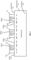
- Figure 1 shows patterns or masks 160 formed on areas 111 of top surface 103.
- Masks 160 may be hardmask patterns formed on first top surface areas or locations 111 of a single crystal (e.g., Si) substrate where top surfaces of the electronic device fins are desired.
- mask 160 is formed by or of photoresist alone, or a photoresist/oxide combination; or a photoresist/nitride combination.
- Mask 160 may have sidewalls 166 and 170 above surface 103. Sidewalls 166 and 170 may be planar surfaces perpendicular to surface 103.
- Areas 111 may have width W1, and length L1 into the page (not shown). In some cases, Areas 111 and masks 160 may have width W1 and Length L1 (not shown but directed into the page of Figure 1 ). Areas 119 may be width W2, and length L1 into the page (not shown). Trenches 105 and 106 are formed below top surface areas 119, between locations where areas 111 or top surfaces of electronic device fins are desired.
- Figure 2 shows the semiconductor substrate of Figure 1 after etching a thickness of the substrate between hardmasks to form sidewalls of the electronic device fins and trenches in the between the hardmasks.
- Figure 2 shows substrate 101 after etching a thickness of material 102 between hard masks 160 or areas 111 to form single crystal sidewalls 113 and fins 107, 108 and 110. In some cases, this etching may include etching a thickness of material 102 between hard masks 160 or areas 111 to create or form single crystal Silicon top surface 103 and sidewalls 113 and 115 of electronic device fins 107, 108 and 110.
- Etching material 102 includes etching surface 103 at areas 119 to form the trenches.
- Length LI may be a length of between 50 nanometers (nm) and 100 micrometers (um). In some cases LI is approximately 500 nm. In some cases LI is equal to (or approximately the same as) W1. According to some embodiments, W1 may be between 10 and 15 nanometers (nm) and HI may be 350 nanometers (nm).
- Trenches 105 and 106 may be formed by patterning and etching as known in the art. This may include patterning and etching material 102 to form the trenches. In some cases, patterning and etching material 102 includes using a resist or hard mask (e.g., 160) underneath a resist for the patterning materials. In some cases 1, 2, or 3 resist layers may be used for the patterning materials. In some cases, patterning and etching material 102 to form the trenches includes using an O2 or O2/Ar plasma etch at pressures in the 10-100mTorr range, and at room temperature.
- Such patterning and etching may also include etching an oxides including STI material, by etching with fluorocarbons (e.g., CF4 and/or C4F8), O2 and Ar, at pressures in the 10-100mTorr range, and at room temperature.
- fluorocarbons e.g., CF4 and/or C4F8
- Sidewalls 113 and 115, and surfaces 203 may be subjected to high energy ion bombardment, oxidation, and/or etch residues, depending on the technique used to etch material 102.
- the sidewalls and bottom surfaces include crystalline defects that would cause a single crystal material epitaxially grown on them to have defects, and reduced transistor performance if the epitaxially grown material was used as a device channel. If these defects propagate throughout the channel material, they can lead to yield and variations issues in a device built on a device layer formed from epitaxial growth extending above the trench.
- material 307 is a layer of shallow trench isolation (STI) material formed or grown on top surfaces 103, 203 (and optionally sidewalls 113 and 115) of the substrate 101.
- Material 307 may be formed of an oxide or a nitride or combination thereof.
- Material 307 may be formed of SiC or another material as known in the art.
- Material 307 may be formed by atomic layer deposition (ALD) or chemical vapor deposition (CVD). Material 307 is generally deposited via Plasma Enhanced Chemical Deposition (PECVD).
- PECVD Plasma Enhanced Chemical Deposition
- any of various oxygen precursors, Silane precursors, or generic precursors can be used during a process (e.g., PECVD) to form Material 307, as known in the art.
- Material 307 may be formed by a process using TEOS + O2 + RF at 400°C.
- fins 407, 408 and 410 may be formed, grown or produced by other processes. In some cases, fins 407, 408 and 410 may be grown from a surface of material 102 in trenches formed in a layer of trench oxide material formed on a surface of substrate 101. In some cases, fins 407, 408 and 410 may be formed, grown or produced by processes know in the art. In some cases, fins 407, 408 and 410 may be conventionally patterned Si fins.
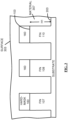
- Figure 5 shows the semiconductor substrate of Figure 1 after etching the top surfaces and the sidewalls of the electronic device fins to form narrower etched single crystal top surfaces and sidewalls of a narrower etched electronic device fins.
- Figure 5 shows substrate 101 after etching top surfaces 403 and sidewalls 113 and 115 of fins 407, 408 and 410 to remove thickness TH2 of material 102 to form "narrower" etched single crystal top surfaces 503 and sidewalls 513 and 515 of narrower etched electronic device fins 507, 508 and 510.
- This etch may include forming fins 507, 508 and 510 having width W3, which is (e.g., extends in width) less than width W1, and having length L1.
- top surface 503 may be at, and fins 507, 508 and 510 may have height H4 above surface 203. Height H4 may be equal to or less than height H2.
- surfaces 503 may be at or below the height of surfaces 403.
- Fins 507, 508 and 510 are shown having height H5 above surface 413 of trench oxide material 417, and above surface 523 of material 102 of substrate 101.
- the etch to form fins 507, 508 and 510 may etch a height of fins 407, 408 and 410 equal to height H5, such that surface 523 is planar with or level with surface 413. In some cases, surface 523 is above or below surface 413.
- the etch to form fins 507, 508 and 510 may be described as a "second" etch (e.g., to form the narrower fins), such as where the etch at Figure 2 or 4 (or block 820 or 845) is considered a "first" etch to form the narrower fins (e.g., prior to the second etch).
- etching the top surfaces and the sidewalls of the electronic device fins includes forming the etched fins by trimming a width of the device fins from greater than 10 nm to 30 nm to a width of the etched fins of less than 7 nm to 15 nm.
- This etch may form surfaces 503 and sidewalls 513 and 515, which do not contain damaged regions due to excessive high energy bombardment, oxidation, or etch residues; such as compared to the etch to form fins 107, 108 and 110; or compared to a dry etch that employs high energy ion bombardment etch (e.g. as known in the art as a physical etch).
- This etch may exclude or not include a dry etch, a high energy ion bombardment etch; or allowing oxidation of, exposure to oxygen, or residue to form on surfaces 503 and sidewalls 513 and 515.
- Such etching may use a "timed” etch, such as an etch for a period of time known to remove thickness TH1 of material 102 from surfaces 406 and sidewalls 113 and 115.
- the fins may be or include an "exposed" device well or channel region extending or disposed above surface 413 or 523.
- Fins 507, 508 and 510 may be described as “narrow” or “narrower” fins, such as fins that result after “wide” or “wider” fins are further etched as noted herein, such as at least with respect to Figure 5 and block 850.
- etching the top surfaces and the sidewalls of the wider electronic device fins includes using thermal processing.
- using chlorine based chemistry may include using low ion energy plasma processing (an unclaimed embodiment of the invention) such as using low energy chlorine containing plasma.
- using chlorine or fluorine based chemistry may include using less than 1 kW of radio frequency energy, such as for between 10 and 40 seconds.
- using thermal processing in presence of HCl may include etching in an epitaxial deposition reactor.
- using thermal processing may include using less than 900 degrees Celsius heat in a wafer processing chamber, such as for between 30 and 120 seconds. Another example is anneal in presence of Cl 2 at a temperature below 700 degrees Celsius for 60 sec.
- Figure 5 may show substrate 101 after forming trimmed fins 507, 508 and 510 fins by introducing substrate 101 having single crystal silicon fins 407, 408 and 410 into an epitaxial deposition tool or in epitaxial reactor to etch those fins down to form single crystal silicon fins 507, 508 and 510.
- the tool may use Cl based chemistry using low ion energy plasma processing (an unclaimed aspect of the invention) or thermal processing to trim the fin width (e.g., width W1 of fins 407, 408 and 410) from greater than 10 nm (e.g., 30, 20 or 15nm) to a width (e.g., width W3 of fins 507, 508 and 510) of 15 nm or below (e.g., 15, 10, 7 nm).
- the low ion energy plasma processing may use an epitaxial deposition tool and a Cl based chemistry using low ion energy plasma processing (an unclaimed aspect of the invention) to achieve a trim etch.
- this etch includes: using low energy Cl containing plasma, using 200 mT, using 10 seem CI 2, using 100 seem H2, using 300 seem Ar, using 500W of radio frequency energy, using ion energy 2 eV, and etching for 20 seconds, for example.
- the thermal processing may use an epitaxial reactor using low heat processing to achieve a trim etch.
- One example of this etch includes: using in epi reactor: using 750 celsius (C), using 100 seem HCl, using 10000 seem H2, using 20 T and etching for 60 seconds, for example.
- Such fins 507, 508 and 510 may be used to form fin devices including fin integrated circuit (IC) transistors, resistors, capacitors, etc. formed in or on sidewalls of "fins” grown from or extending above a semiconductor (e.g., silicon) substrate or other material.
- Such devices may include fin metal oxide semiconductor (MOS) transistor devices, such as those used in a complementary metal oxide semiconductor (CMOS) based on movement of electrons in N-type (e.g., doped to have electron charge carriers) MOS device (n-MOS) channels and movement of positive charged holes in P-type (e.g., doped to have hole charge carriers) MOS device (p-MOS) channels.
- MOS fin metal oxide semiconductor
- top surfaces and sidewalls of fins 507, 508 and 510 have or maintain the same atomic lattice and crystal structure as that of fins 407, 408 and 410, but contain fewer surface crystal defects, less ion damage, less oxidation and less etch residues than that of fins 407, 408 and 410.
- a thermal treatment may be or include an all chemical, no plasma etch that uses HCl Cl 2 for example at a high enough temperature that converts the silicon atoms on the surface when the chlorine interacts with those silicon atoms to form SiCl 4 gas which is then pumped out of the chamber during treatment, but does not use a high enough temperature to damage or amorphize the crystal lattice of exposed surfaces of the etched fin 507.
- the thermal etch may be or include a dynamic treatment with no plasma, and be at less than 900 degrees Celsius. In some cases, in this recipe no physical sputtering occurs but the chlorine reacts to form SiCl 4 gas which evaporates away from the Si surfaces and is pumped out.
- the wide single crystal top surfaces and the wide sidewalls with width W1 may have a thickness of between a 5 nm and 15 nm greater than a thickness of the narrower single crystal top surfaces and the narrower sidewalls with width W3.
- the narrower upper fin portion 582 may be exposed above the first thickness H3 of trench oxide material 417 in the trenches.
- portion 584 may be described as sub-channel. In some cases, portion 582 is the channel and hence may conduct most of the carriers while portion 584 will be far from the gate electrode and will not be part of the channel.
- Figure 5 provides embodiments where the fins are trimmed and no additional cladding layer is added.
- these narrower tins can be used to create transistors that will be improved by virtue of the better electrostatics of the narrow fin versus an equivalent device with a wide fin.
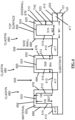
- Figure 6 shows the semiconductor substrate of Figure 1 after depositing a second single crystal material on the etched top and sidewall surfaces of the narrower etched fins.
- SiGe or Ge deposition of material 620 is performed on substrate 101 (e.g., on fins 507, 508 and 510), such as is shown in Figure 6 .
- Figure 6 shows epitaxial layer 620 deposited on trimmed fins 507, 508 and 510.
- Layer 620 may be a second crystal structure grown from the single crystal structure of material 102 at top surface 503 and from sidewalls 513 and 515.
- Figure 6 shows substrate 101 after depositing or growing single crystal material or layer 620 on fins 507, 508 and 510.
- Material 620 may be epitaxially grown from or on surfaces 503 and sidewalls 513 and 515. Material 620 may be thickness TH2 at surface 503 and sidewalls 513 and 515. Material 620 may be epitaxially grown as a "blanket" layer on surface 503 and sidewalls 513 and 515. Material 620 may have top surface 655 and sidewalls 666 and 676. Surface 655 may be of height H6 of the surface 413.
- Material 620 may be a single crystal material that is the same as or different than the single crystal material 202 of substrate 101.
- material 620 may be formed by selective growth, such as by a CVD type of growth, gas source-molecular beam epitaxy (GS-MBE), rapid thermal (RT) CVD, or ultra high vacuum (UHV)-CVD.
- GS-MBE gas source-molecular beam epitaxy
- RT rapid thermal
- UHV ultra high vacuum
- the growth of material 620 is grown selectively from material 102 by choosing or using a predetermined growth temperature range, pressure, gas flux range, etc., as known for material 620 to grow from material 102, but not grow from or initiate on material of the oxide surfaces.
- material 620 may be a "cladding" material that is “selectively” grown only from a desired single crystal material (e.g., surfaces 503 and sidewalls 513 and 515) but not from other polycrystal, dielectric, oxide, nitride or amorphouse exposed materials (e.g., that are not the desired or are not a single crystal material).
- a "cladding" material e.g., material 620
- material 620 may be “selectively” grown only from a desired single crystal material (e.g., surfaces 503 and sidewalls 513 and 515) by masking or forming oxide layers over materials that it is not desired to have the "cladding" material form or grow from.
- material 620 is a selectively grown epitaxial layer.
- material 102 is single crystal Si material; and material 620 is a layer of single crystal SiGe material (e.g., 70 percent Si, and 30 percent Ge) such as for an P-type device formed from fin 245.
- material 620 is a layer of single crystal SiGe material (e.g., 30 percent Si, and 70 percent Ge) such as for an P-type device formed from fin 245.
- material 620 is a channel material or layer for a tri-gate device having the channel conducting charges mostly along or through material 620. This may include conducting charges mostly along or through top surface 655 and sidewalls 666 and 676.
- Fins 680 may be used to form fin devices including fin integrated circuit (IC) transistors, resistors, capacitors, etc. formed in or on sidewalls of "fins" grown from or extending above a semiconductor (e.g., silicon) substrate or other material.
- Such devices may include fin metal oxide semiconductor (MOS) transistor devices, such as those used in a complementary metal oxide semiconductor (CMOS) based on movement of electrons in N-type (e.g., doped to have electron charge carriers) MOS device (n-MOS) channels and movement of positive charged holes in P-type (e.g., doped to have hole charge carriers) MOS device (p-MOS) channels.
- MOS fin metal oxide semiconductor
- equipment for forming fins 107, 407, 507 and 680 may include equipment from suppliers that are configured into a system including various chambers and vessels that have a vacuum sealed environment, and a robot for moving wafers between the various chambers.
- the "in-situ" methods herein may include keeping or maintaining substrate 101 and fins within these vessels or within this vacuum environment (e.g., system) so that the substrate and fins are not exposed to air although they may be moved into different chambers of the system, such as by being moved to chambers of the same equipment set without breaking the vacuum seal of the chambers, or without an "air break" during movement of the substrate between chambers.
- Figure 7 is a schematic perspective view of the semiconductor substrate of Figure 1 after forming a gate electronic device on the second single crystal material formed on the etched top and sidewall surfaces of one of the narrower etched fins.
- Figure 7 shows cross sectional view perspective A- A, which may be the perspective of Figures 1-6 .
- FIG. 7 may schematically illustrate a perspective view of transistor device 700, in accordance with some embodiments.
- Figure 7 shows substrate 101 after forming gate electronics device 700 on material 620 formed on surfaces 503 and sidewalls 513 and 515 of narrower etched fins 507, 508 and 510.
- Device 700 may have a narrow channel 702 that is or includes fin 680. Fin 680 has length LI, width W4 and height H6 above surface 413 or 523.
- Narrow channel 702 may have top surface 655 and sidewalls 666 and 676.
- a gate dielectric (not shown) may be formed over surface 655 and sidewalls 666 and 676 under gate electrode 704, spacers 706 may be formed on or beside gate electrode 704.
- Mass 708 may be formed on the top surface of gate electrode 704.
- Mask 708 may be a hard mask that can be removed to form a metal gate contact.
- Device 700 includes fin 680 and may be formed on material 417.
- device 700 is a PMOS device formed from the clad electronic device fin 680, wherein the PMOS device include gate 701 on second single crystal material 620; and junction regions (not shown) on both sides and adjacent to the gate and in the second single crystal material.
- the semiconductor substrate 101 may be composed of Si in some embodiments.
- the semiconductor substrate 101 may include n-type or p-type (100) off-oriented Si, the crystalline directions of the semiconductor substrate 101 being symbolized by the convention (xyz), where x, y, and z represent respective crystallographic planes in three dimensions that are perpendicular to one another.
- the semiconductor substrate 101 may, for example, include material of a (100) direction off-cut in a range between about 2 degrees to about 8 degrees towards a (110) direction. Other off-cut orientations or a semiconductor substrate 101 without an off-cut orientation may be used.
- the semiconductor substrate 101 may have a high resistivity between about 1 ⁇ -cm to about 50 k ⁇ -cm.
- the semiconductor substrate 101 may include other materials in other embodiments.
- the semiconductor substrate 101 is part of a cingulated die of a wafer.
- the semiconductor substrate is a p-type substrate.
- the SiGe material 620 of the fin structure 680 may be formed by etching fin 407 (or 107) to form narrower fin 507 and depositing a transistor element such as, for example, the material 620 using techniques described herein. In some embodiments, only a portion of the fin structure 680 is covered with material 620.
- the Si tin 507 of the fin structure 680 may be composed of a defect- free single crystal in some embodiments. In other embodiments, most or all of the transistor element (e.g., tin structure 680) may be covered with material 620.
- the transistor device 700 may be p-type or n-type.
- the channel body formed using the SiGe material 620 may provide greater mobility of mobile charge carriers for p-type. For example, increasing a concentration of germanium (Ge) in the channel body may increase mobility of electrons or holes by nature of the material.
- a second mechanism causes further increase in the mobility of the holes in the p-channel (e.g., channel of PMOS device) by providing a compressive strain to the channel body because the lattice spacing of the Si material 102 is smaller than that of the SiGe or Ge material 620, thus causing a compressive strain in material 620 where a majority of the carriers flow through the channel.
- the transistor device 700 is p-type (e.g., PMOS device).
- the PMOS device may have a p- channel that is doped n-type and the NMOS device may have an n-channel that is doped p-type.
- dielectric materials examples include, but are not limited to, silicon oxide, carbon doped oxide (CDO), silicon nitride, organic polymers such as perfluorocyclobutane or polytetrafluoroethylene, fluorosilicate glass (FSG), and organosilicates such as silsesquioxane, siloxane, or organosilicate glass.
- CDO carbon doped oxide
- FSG fluorosilicate glass
- organosilicates such as silsesquioxane, siloxane, or organosilicate glass.
- an annealing process may be carried out on the gate dielectric (not shown, but between electrode 704 and surface 655 and sidewalls 666 and 676) to improve its quality when a high-k material is used.
- the gate dielectric (not shown, but between electrode 704 and surface 655 and sidewalls 666 and 676) may include a dummy oxide that is subsequently removed in a process How together with a dummy gate electrode and replaced with a high-k gate dielectric and metal gate, according to well-known techniques.
- the gate electrode 704 may be formed on the gate dielectric (not shown, but between electrode 704 and surface 655 and sidewalls 666 and 676) and may be composed of at least one p-type workfunction metal or n-type workfunction metal, depending on whether the transistor is to be a PMOS (e.g., p-type) or an NMOS (e.g., n-type) transistor.
- the gate electrode 704 may consist of two or more metal layers, where at least one metal layer is a workfunction metal layer and at least one metal layer is a fill metal layer.
- the gate electrode 704 is a polysilicon gate electrode.
- the gate electrode 704 is a dummy polysilicon gate electrode that is subsequently removed in a process flow and replaced with a metal gate electrode, according to well-known techniques.
- metals that may be used for the gate electrode include, but are not limited to, ruthenium, palladium, platinum, cobalt, nickel, and conductive metal oxides, e.g., ruthenium oxide.
- a p-type metal layer may enable the formation of a PMOS gate electrode with a workfunction that is between about 4.9 eV and about 5.2 eV.
- metals that may be used for the gate electrode 704 include, but are not limited to, hafnium, zirconium, titanium, tantalum, aluminum, alloys of these metals, and carbides of these metals such as hafnium carbide, zirconium carbide, titanium carbide, tantalum carbide, and aluminum carbide.
- An n-type metal layer may enable the formation of an NMOS gate electrode with a workfunction that is between about 3.9 eV and about 4.2 eV.
- the transistor device 700 of FIG. 7 depicts a tri-gate configuration.
- similar principles and techniques as described herein for converting a transistor element from Si to SiGe may be used for other transistor configurations including, for example, planar, dual-gate, all around gate (AAG) (also referred to as gate all around), wire (e.g., nanowire), and other suitable transistor configurations.
- AAG all around gate
- wire e.g., nanowire
- Figure 8 is an example process tor forming a gate electronic device on a second single crystal material formed on narrower etched single crystal top and sidewall surfaces of a narrower etched electronic device fin.
- Figure 8 may show process 800 for forming fins 507, 508 and 5 10.
- process 800 is a process performing clad fins 680.
- the process is 800 is or includes part of a process for forming device 700.
- a thickness of the trench oxide material and the hardmasks are polished down to form the top surfaces of the electronic device fins. This may include removing a thickness of material 370 and hardmasks 160 to expose surfaces 403 as described herein. This may include removing all of hardmasks 160 (e.g., of block 810) as described herein. Block 840 may include descriptions herein for Figure 4 .
- the top surfaces and the sidewalls of the electronic device fins are (e.g., simultaneously) etched to form single crystal defect free etched top surfaces and etched sidewalls of electronic device etched fins.
- This may include etching to remove a thickness of between a 5 nm and 15 nm of the top surfaces and the sidewalls of the electronic device fins.
- This may include simultaneously etching top surfaces 403 and the sidewalls 113 and 115 of electronic device fins 407 and 408 (e.g., simultaneously) to form single crystal defect free etched top surfaces 503 and the sidewalls 513 and 515 of narrower electronic device fins 507 and 508 as described herein.
- Block 850 may include descriptions herein for Figure 5 .
- Block 850 may include etching the top surfaces and the sidewalls of the electronic device fins to form narrower etched single crystal top surfaces and sidewalls of a narrower etched electronic device fins.
- block 850 includes maintaining (e.g., not creating defects in) the single crystal structure of the top and sidewall surfaces of the device fins of the etched top surfaces 503 and the sidewalls 513 and 515.
- the etch to form fins 507 and 508, may be described as a "second" etch (e.g., to form the narrower fins), such as where the etch at Figure 2 or 4 (or block 820 or 845) is considered a "first" etch to form the narrower fins (e.g., prior to the second etch).
- block 850 includes etching the top surfaces and the sidewalls of the electronic device fins using one of (1) chlorine based chemistry using low ion energy plasma processing (an unclaimed aspect of the invention), or (2) thermal processing.
- etching the top surfaces and the sidewalls of the electronic device fins includes forming the etched fins by trimming a width of the device fins from greater than 10 nm to 30 nm to a width of the etched fins of less than 7 nm to 15 nm.
- a second single crystal material is deposited on or grown from the top and sidewall surfaces of the etched narrow fins (e.g., of block 850). This may include the second single crystal material being deposited on or grown, without air break of the treatment chamber after etching the top surfaces and the sidewalls of the electronic device fins in block 850.
- the second single crystal material may have a lattice spacing that is different (e.g., larger) than a lattice spacing of the first single crystal material.
- This may include, without air break of the treatment chamber after etching to form narrower fins 507 and 508, depositing second single crystal material 620 on the top surfaces 503 and sidewalls 513 and 515 of the etched narrower fins, wherein the second single crystal material has a lattice spacing that is different than a lattice spacing of the first single crystal material as described herein.
- Block 860 may include descriptions herein for Figure 6 .
- a gate is formed over the second single crystal material, and junction regions are formed in the second single crystal material adjacent to and on either side of the gate.
- This may include forming gate 701 over the second single crystal material 620, and forming junction regions in the second single crystal material 620 as described herein.
- This may include forming a cladding of SiGe material 620 of the fin structure 680 may be formed by etching fin 407 (or 107) to form narrower Si fin 507 and depositing a transistor element such as, for example, the material 620 as described herein. This may include forming part of or all of device 700 as described herein.
- Block 870 may include descriptions herein for Figure 7 .
- the processes described herein may avoid or reduce high energy ion bombardment, oxidation and etch residues on Silicon fin surfaces, which are damaging to the quality of subsequently clad or deposited layers. Consequently, the crystaline structure of subsequently clad or deposited layer growth will not include defects due to the defects in or additional material upon the crystaline structure of the silicon fin top and sidewall surfaces. That growth may provide electronic device material (e.g., wells and/or channels) in which defect free fin based devices and transistors may be formed. Thus, avoiding or reducing such bombardment, oxidation and residues increases transistor performance.
- Such transistors may include finfets, Ge cladding, SiGe channels, SiGe cladding, trigate transistors.
- Such transistors may be produced by High Volume Architecture and may be embodied in computer system architecture features and interfaces made in high volumes. Such transistors may be included in or formed by very large scale integration (VLSI) logic processes.
- VLSI very large scale integration
- computing device 900 may include other components that may or may not be physically and electrically connected to board 902. These other components include, but are not limited to, volatile memory (e.g., DRAM), non-volatile memory (e.g., ROM), flash memory, a graphics processor, a digital signal processor, a crypto processor, a chipset, an antenna, a display, a touchscreen display, a touchscreen controller, a battery, an audio codec, a video codec, a power amplifier, a global positioning system (GPS) device, a compass, an accelerometer, a gyroscope, a speaker, a camera, and a mass storage device (such as hard disk drive, compact disk (CD), digital versatile disk (DVD), and so forth).
- volatile memory e.g., DRAM
- non-volatile memory e.g., ROM
- flash memory e.g., a graphics processor, a digital signal processor, a crypto processor, a chipset, an antenna, a
- Communication chip 906 enables wireless communications for the transfer of data to and from computing device 900.
- wireless and its derivatives may be used to describe circuits, devices, systems, methods, techniques, communications channels, etc., that may communicate data through the use of modulated electromagnetic radiation through a non-solid medium. The term does not imply that the associated devices do not contain any wires, although in some embodiments they might not.
- a first communication chip 906 may be dedicated to shorter range wireless communications such as Wi-Fi and Bluetooth and a second communication chip 906 may be dedicated to longer range wireless communications such as GPS, EDGE, GPRS, CDMA, WiMAX, LTE, Ev-DO, and others.
- Processor 904 of computing device 900 includes an integrated circuit die packaged within processor 904.
- the integrated circuit die includes transistors formed by epitaxially growing second crystal material 620 on surfaces of etched, thinned first crystal material fins (e.g., 507, 508 and 510) formed by etching wider fins of the first crystal material, such as described with reference to Figures 1-8 .
- the integrated circuit die includes electronic device fins having narrower upper fin portion 582 formed on and from wide lower fin portion 584, such as described with reference to Figures 1-8 .
- the term "processor" may refer to any device or portion of a device that processes electronic data from registers and/or memory to transform that electronic data into other electronic data that may be stored in registers and/or memory.
- Communication chip 906 also includes an integrated circuit die packaged within communication chip 906.
- a package including a communication chip incorporates one or more fin devices having transistors formed by epitaxially growing a second crystal material on surfaces of etched, thinned first crystal material fins formed by etching wider fins of the first crystal material such as described above.
- another component housed within computing device 900 may contain a microelectronic package including a fin device having cladding device layers such as described above.
- computing device 900 may be a laptop, a netbook, a notebook, an ultrabook, a smartphone, a tablet, a personal digital assistant (PDA), an ultra mobile PC, a mobile phone, a desktop computer, a server, a printer, a scanner, a monitor, a set-top box, an entertainment control unit, a digital camera, a portable music player, or a digital video recorder.
- computing device 900 may be any other electronic device that processes data.
Landscapes
- Insulated Gate Type Field-Effect Transistor (AREA)
- Metal-Oxide And Bipolar Metal-Oxide Semiconductor Integrated Circuits (AREA)
- Chemical & Material Sciences (AREA)
- Thin Film Transistor (AREA)
- Chemical Kinetics & Catalysis (AREA)
- General Chemical & Material Sciences (AREA)
- Crystallography & Structural Chemistry (AREA)
- Drying Of Semiconductors (AREA)
Claims (4)
- Procédé destiné à former des ailerons de dispositif électronique dans une ou plusieurs chambres qui ont un environnement scellé sous vide, le procédé comprenant :la suppression par gravure d'une épaisseur d'un substrat (101) entre de premières zones de la surface supérieure d'un substrat d'un premier matériau monocristallin pour former de larges ailerons de dispositif électronique (110) sous les premières zones de la surface supérieure et pour former des tranchées (105, 106) entre les premières zones de la surface supérieure, les larges ailerons de dispositif électronique ayant de larges surfaces supérieures monocristallines et de larges parois latérales ;la formation d'une première épaisseur d'un matériau à base d'oxyde en tranchée (417) dans les tranchées et sous les premières zones de la surface supérieure ;la gravure d'une épaisseur des larges surfaces supérieures monocristallines et des larges parois latérales des larges ailerons de dispositif électronique pour former des ailerons de dispositif électronique plus étroits (507, 508, 510) à partir des larges ailerons, les ailerons de dispositif électronique plus étroits ayant des surfaces supérieures monocristallines plus étroites et des parois latérales plus étroites avec un réseau monocristallin identique à celui des larges surfaces supérieures monocristallines et des larges parois latérales, la gravure de l'épaisseur des larges surfaces supérieures monocristallines et des larges parois latérales comportant le retrait d'une épaisseur comprise entre 1 nm et 15 nm des larges surfaces supérieures monocristallines et des larges parois latérales, ladite gravure comprenant une gravure par traitement thermique,le traitement thermique comportant l'utilisation de courants de HCl ou Cl2 gazeux dans un environnement d'hydrogène à des températures inférieures à 900 °C ou 700 °C, respectivement ; etaprès la gravure de l'épaisseur des larges surfaces supérieures monocristallines et des larges parois latérales, sans cassage du vide d'une chambre, le dépôt d'un deuxième matériau monocristallin (620) sur les surfaces supérieures amincies et les parois latérales amincies pour former des ailerons de dispositif électronique revêtus, le deuxième matériau monocristallin ayant une constante de réseau qui est plus grande qu'une constante de réseau du premier matériau monocristallin.
- Procédé selon la revendication 1, comprenant en outre :avant la suppression par gravure de l'épaisseur du substrat, la formation de motifs de masque dur sur les premières zones de la surface supérieure du substrat monocristallin là où des surfaces supérieures des ailerons de dispositif électronique sont souhaitées ; puisaprès la suppression par gravure de l'épaisseur du substrat, le retrait des masques durs ; puisle dépôt d'une deuxième épaisseur d'un matériau à base d'oxyde en tranchée dans les tranchées formées par suppression par gravure de l'épaisseur du substrat entre les premières zones de la surface supérieure ; puisun polissage pour retirer une troisième épaisseur du matériau à base d'oxyde en tranchée au-dessus des premières zones de la surface supérieure ; et puisavant la gravure de l'épaisseur des larges surfaces supérieures monocristallines et des larges parois latérales, la suppression par gravure d'une quatrième épaisseur du matériau à base d'oxyde en tranchée dans les tranchées pour exposer les larges parois latérales monocristallines des larges ailerons de dispositif électronique et pour former la première épaisseur d'un matériau à base d'oxyde en tranchée.
- Procédé selon la revendication 1, dans lequel la gravure des larges surfaces supérieures et des larges parois latérales comprend la conservation dans les surfaces supérieures monocristallines plus étroites et les parois latérales plus étroites d'une structure de réseau monocristallin des larges surfaces supérieures et des larges parois latérales.
- Procédé selon la revendication 1, dans lequel une largeur des ailerons de dispositif électronique revêtus est égale ou inférieure à 20 nm de large.
Applications Claiming Priority (1)
| Application Number | Priority Date | Filing Date | Title |
|---|---|---|---|
| PCT/US2013/077593 WO2015099680A1 (fr) | 2013-12-23 | 2013-12-23 | Pré-sculpture d'éléments ailettes en si avant revêtement pour applications sur canaux de transistor |
Publications (3)
| Publication Number | Publication Date |
|---|---|
| EP3087590A1 EP3087590A1 (fr) | 2016-11-02 |
| EP3087590A4 EP3087590A4 (fr) | 2017-11-22 |
| EP3087590B1 true EP3087590B1 (fr) | 2025-04-09 |
Family
ID=53479355
Family Applications (1)
| Application Number | Title | Priority Date | Filing Date |
|---|---|---|---|
| EP13900420.4A Active EP3087590B1 (fr) | 2013-12-23 | 2013-12-23 | Pré-sculpture d'éléments ailettes en si avant revêtement pour applications sur canaux de transistor |
Country Status (6)
| Country | Link |
|---|---|
| US (3) | US9653584B2 (fr) |
| EP (1) | EP3087590B1 (fr) |
| KR (1) | KR102175547B1 (fr) |
| CN (1) | CN105874573B (fr) |
| TW (3) | TWI597781B (fr) |
| WO (1) | WO2015099680A1 (fr) |
Families Citing this family (21)
| Publication number | Priority date | Publication date | Assignee | Title |
|---|---|---|---|---|
| US9954104B2 (en) * | 2014-01-24 | 2018-04-24 | Globalfoundries Inc. | Multiwidth finFET with channel cladding |
| KR102274750B1 (ko) * | 2015-01-27 | 2021-07-07 | 삼성전자주식회사 | 반도체 장치 제조 방법 |
| TWI671819B (zh) * | 2015-07-01 | 2019-09-11 | United Microelectronics Corp. | 半導體裝置及其製作方法 |
| US9698225B2 (en) * | 2015-07-07 | 2017-07-04 | International Business Machines Corporation | Localized and self-aligned punch through stopper doping for finFET |
| US9899387B2 (en) * | 2015-11-16 | 2018-02-20 | Taiwan Semiconductor Manufacturing Company, Ltd. | Multi-gate device and method of fabrication thereof |
| US9431486B1 (en) | 2015-11-30 | 2016-08-30 | International Business Machines Corporation | Channel strain and controlling lateral epitaxial growth of the source and drain in FinFET devices |
| US9997615B2 (en) * | 2015-11-30 | 2018-06-12 | Taiwan Semiconductor Manufacturing Co., Ltd. | Method for forming semiconductor structure with epitaxial growth structure |
| US10109739B2 (en) * | 2016-04-15 | 2018-10-23 | Taiwan Semiconductor Manufacturing Co., Ltd. | Fin field effect transistor |
| US10431684B2 (en) * | 2016-04-22 | 2019-10-01 | Texas Instruments Incorporated | Method for improving transistor performance |
| CN108878525A (zh) * | 2017-05-09 | 2018-11-23 | 中芯国际集成电路制造(上海)有限公司 | 鳍式结构的制作方法 |
| US9991262B1 (en) | 2017-06-15 | 2018-06-05 | Taiwan Semiconductor Manufacturing Co., Ltd. | Semiconductor device on hybrid substrate and method of manufacturing the same |
| DE112017007838T5 (de) * | 2017-09-28 | 2020-05-07 | Intel Corporation | Transistoren mit kanal- und unterkanalregionen mit unterschiedlichen zusammensetzungen und abmessungen |
| KR20250070116A (ko) * | 2017-11-30 | 2025-05-20 | 인텔 코포레이션 | 진보된 집적 회로 구조체 제조를 위한 핀 패터닝 |
| US10818800B2 (en) * | 2017-12-22 | 2020-10-27 | Nanya Technology Corporation | Semiconductor structure and method for preparing the same |
| CN110047926B (zh) * | 2018-01-15 | 2023-08-29 | 联华电子股份有限公司 | 半导体装置以及其制作方法 |
| US10332999B1 (en) * | 2018-03-09 | 2019-06-25 | International Business Machines Corporation | Method and structure of forming fin field-effect transistor without strain relaxation |
| US11004852B2 (en) * | 2018-10-30 | 2021-05-11 | Taiwan Semiconductor Manufacturing Co., Ltd. | Semiconductor structure |
| US10998311B2 (en) * | 2019-06-28 | 2021-05-04 | International Business Machines Corporation | Fabricating gate-all-around transistors having high aspect ratio channels and reduced parasitic capacitance |
| KR102742581B1 (ko) | 2019-09-24 | 2024-12-13 | 삼성전자주식회사 | 반도체 소자 및 이의 제조 방법 |
| DE102020107241B4 (de) | 2019-10-29 | 2025-02-06 | Taiwan Semiconductor Manufacturing Co., Ltd. | Finnen-feldeffekttransistor-bauelement und verfahren zu dessen herstellung |
| US11482421B2 (en) * | 2019-10-29 | 2022-10-25 | Taiwan Semiconductor Manufacturing Co., Ltd. | Method of forming a semiconductor device by a replacement gate process |
Citations (3)
| Publication number | Priority date | Publication date | Assignee | Title |
|---|---|---|---|---|
| US20050104091A1 (en) * | 2003-11-04 | 2005-05-19 | Tabery Cyrus E. | Self aligned damascene gate |
| US20090090934A1 (en) * | 2007-10-05 | 2009-04-09 | Tsutomu Tezuka | Field Effect Transistor and Method for Manufacturing the Same |
| WO2015094167A1 (fr) * | 2013-12-16 | 2015-06-25 | Intel Corporation | Dispositifs nmos et pmos contraints exempts de substrats relaxés |
Family Cites Families (10)
| Publication number | Priority date | Publication date | Assignee | Title |
|---|---|---|---|---|
| KR100517559B1 (ko) | 2003-06-27 | 2005-09-28 | 삼성전자주식회사 | 핀 전계효과 트랜지스터 및 그의 핀 형성방법 |
| US7250645B1 (en) | 2004-01-22 | 2007-07-31 | Advanced Micro Devices, Inc. | Reversed T-shaped FinFET |
| CN101853882B (zh) | 2009-04-01 | 2016-03-23 | 台湾积体电路制造股份有限公司 | 具有改进的开关电流比的高迁移率多面栅晶体管 |
| JP5166458B2 (ja) | 2010-01-22 | 2013-03-21 | 株式会社東芝 | 半導体装置及びその製造方法 |
| US8492235B2 (en) * | 2010-12-29 | 2013-07-23 | Globalfoundries Singapore Pte. Ltd. | FinFET with stressors |
| DE112011105996B4 (de) * | 2011-12-22 | 2023-11-16 | Intel Corporation | Halbleiterbauelement mit einem verengten Halbleiterkörper |
| TW201335986A (zh) * | 2012-02-23 | 2013-09-01 | United Microelectronics Corp | 鰭狀結構及其形成方法 |
| US9012286B2 (en) * | 2012-04-12 | 2015-04-21 | Globalfoundries Inc. | Methods of forming FinFET semiconductor devices so as to tune the threshold voltage of such devices |
| US8729634B2 (en) * | 2012-06-15 | 2014-05-20 | Taiwan Semiconductor Manufacturing Company, Ltd. | FinFET with high mobility and strain channel |
| US9627245B2 (en) * | 2014-03-05 | 2017-04-18 | Globalfoundries Inc. | Methods of forming alternative channel materials on a non-planar semiconductor device and the resulting device |
-
2013
- 2013-12-23 EP EP13900420.4A patent/EP3087590B1/fr active Active
- 2013-12-23 CN CN201380081077.XA patent/CN105874573B/zh active Active
- 2013-12-23 US US15/037,644 patent/US9653584B2/en active Active
- 2013-12-23 WO PCT/US2013/077593 patent/WO2015099680A1/fr not_active Ceased
- 2013-12-23 KR KR1020167013242A patent/KR102175547B1/ko active Active
-
2014
- 2014-11-21 TW TW103140473A patent/TWI597781B/zh active
- 2014-11-21 TW TW106119474A patent/TWI657507B/zh active
- 2014-11-21 TW TW107120386A patent/TWI703641B/zh active
-
2017
- 2017-04-13 US US15/487,272 patent/US10014412B2/en active Active
-
2018
- 2018-05-30 US US15/993,535 patent/US10396203B2/en active Active
Patent Citations (4)
| Publication number | Priority date | Publication date | Assignee | Title |
|---|---|---|---|---|
| US20050104091A1 (en) * | 2003-11-04 | 2005-05-19 | Tabery Cyrus E. | Self aligned damascene gate |
| US20090090934A1 (en) * | 2007-10-05 | 2009-04-09 | Tsutomu Tezuka | Field Effect Transistor and Method for Manufacturing the Same |
| WO2015094167A1 (fr) * | 2013-12-16 | 2015-06-25 | Intel Corporation | Dispositifs nmos et pmos contraints exempts de substrats relaxés |
| EP3084812B1 (fr) * | 2013-12-16 | 2020-08-12 | Intel Corporation | Dispositifs nmos et pmos contraints exempts de substrats relaxés |
Also Published As
| Publication number | Publication date |
|---|---|
| KR20160101900A (ko) | 2016-08-26 |
| TW201907485A (zh) | 2019-02-16 |
| US20190006508A1 (en) | 2019-01-03 |
| US10396203B2 (en) | 2019-08-27 |
| TW201735173A (zh) | 2017-10-01 |
| EP3087590A4 (fr) | 2017-11-22 |
| CN105874573B (zh) | 2020-04-28 |
| TWI657507B (zh) | 2019-04-21 |
| TWI703641B (zh) | 2020-09-01 |
| CN105874573A (zh) | 2016-08-17 |
| US10014412B2 (en) | 2018-07-03 |
| US20160308032A1 (en) | 2016-10-20 |
| WO2015099680A1 (fr) | 2015-07-02 |
| TW201535527A (zh) | 2015-09-16 |
| US9653584B2 (en) | 2017-05-16 |
| TWI597781B (zh) | 2017-09-01 |
| EP3087590A1 (fr) | 2016-11-02 |
| US20170222035A1 (en) | 2017-08-03 |
| KR102175547B1 (ko) | 2020-11-06 |
Similar Documents
| Publication | Publication Date | Title |
|---|---|---|
| US10396203B2 (en) | Pre-sculpting of Si fin elements prior to cladding for transistor channel applications | |
| CN106030813B (zh) | 在用于晶体管沟道应用的置换栅极工艺期间的鳍状物雕刻和包覆 | |
| EP3314644B1 (fr) | Gravure de canal de remplacement pour interface de haute qualité | |
| TWI727950B (zh) | 替代通道鰭式場效電晶體中之子鰭側壁鈍化 | |
| US9633835B2 (en) | Transistor fabrication technique including sacrificial protective layer for source/drain at contact location | |
| KR102501128B1 (ko) | 희생 코어 상의 클래딩을 통한 트랜지스터 핀 형성 | |
| WO2015199655A1 (fr) | Techniques de formation de transistors à canal ge/sige et à canal iii-v sur la même puce | |
| EP3440706B1 (fr) | Transistor à performances thermiques améliorées | |
| US10483353B2 (en) | Transistor including tensile-strained germanium channel | |
| WO2016190858A1 (fr) | Appareil et procédés de création d'un circuit tampon qui s'étend dans une région commandée par porte d'un transistor |
Legal Events
| Date | Code | Title | Description |
|---|---|---|---|
| PUAI | Public reference made under article 153(3) epc to a published international application that has entered the european phase |
Free format text: ORIGINAL CODE: 0009012 |
|
| 17P | Request for examination filed |
Effective date: 20160517 |
|
| AK | Designated contracting states |
Kind code of ref document: A1 Designated state(s): AL AT BE BG CH CY CZ DE DK EE ES FI FR GB GR HR HU IE IS IT LI LT LU LV MC MK MT NL NO PL PT RO RS SE SI SK SM TR |
|
| AX | Request for extension of the european patent |
Extension state: BA ME |
|
| RIN1 | Information on inventor provided before grant (corrected) |
Inventor name: AUBERTINE, DANIEL B. Inventor name: GLASS, GLENN A. Inventor name: MURTHY, ANAND S. Inventor name: JOSHI, SUBHASH M. |
|
| DAX | Request for extension of the european patent (deleted) | ||
| RIC1 | Information provided on ipc code assigned before grant |
Ipc: H01L 21/336 20060101AFI20170711BHEP Ipc: H01L 29/78 20060101ALI20170711BHEP Ipc: H01L 29/10 20060101ALI20170711BHEP |
|
| A4 | Supplementary search report drawn up and despatched |
Effective date: 20171019 |
|
| RIC1 | Information provided on ipc code assigned before grant |
Ipc: H01L 29/10 20060101ALI20171013BHEP Ipc: H01L 29/78 20060101ALI20171013BHEP Ipc: H01L 21/336 20060101AFI20171013BHEP |
|
| STAA | Information on the status of an ep patent application or granted ep patent |
Free format text: STATUS: EXAMINATION IS IN PROGRESS |
|
| 17Q | First examination report despatched |
Effective date: 20200525 |
|
| RAP1 | Party data changed (applicant data changed or rights of an application transferred) |
Owner name: TAHOE RESEARCH, LTD. |
|
| REG | Reference to a national code |
Ref country code: DE Ref legal event code: R079 Free format text: PREVIOUS MAIN CLASS: H01L0021336000 Ipc: H01L0029660000 Ref country code: DE Ref legal event code: R079 Ref document number: 602013086663 Country of ref document: DE Free format text: PREVIOUS MAIN CLASS: H01L0021336000 Ipc: H01L0029660000 |
|
| GRAP | Despatch of communication of intention to grant a patent |
Free format text: ORIGINAL CODE: EPIDOSNIGR1 |
|
| STAA | Information on the status of an ep patent application or granted ep patent |
Free format text: STATUS: GRANT OF PATENT IS INTENDED |
|
| RIC1 | Information provided on ipc code assigned before grant |
Ipc: H01L 29/10 20060101ALI20241202BHEP Ipc: H01L 29/78 20060101ALI20241202BHEP Ipc: H01L 29/66 20060101AFI20241202BHEP |
|
| INTG | Intention to grant announced |
Effective date: 20241223 |
|
| GRAS | Grant fee paid |
Free format text: ORIGINAL CODE: EPIDOSNIGR3 |
|
| GRAA | (expected) grant |
Free format text: ORIGINAL CODE: 0009210 |
|
| STAA | Information on the status of an ep patent application or granted ep patent |
Free format text: STATUS: THE PATENT HAS BEEN GRANTED |
|
| AK | Designated contracting states |
Kind code of ref document: B1 Designated state(s): AL AT BE BG CH CY CZ DE DK EE ES FI FR GB GR HR HU IE IS IT LI LT LU LV MC MK MT NL NO PL PT RO RS SE SI SK SM TR |
|
| REG | Reference to a national code |
Ref country code: GB Ref legal event code: FG4D |
|
| REG | Reference to a national code |
Ref country code: DE Ref legal event code: R096 Ref document number: 602013086663 Country of ref document: DE |
|
| REG | Reference to a national code |
Ref country code: IE Ref legal event code: FG4D |
|
| REG | Reference to a national code |
Ref country code: NL Ref legal event code: MP Effective date: 20250409 |
|
| PG25 | Lapsed in a contracting state [announced via postgrant information from national office to epo] |
Ref country code: NL Free format text: LAPSE BECAUSE OF FAILURE TO SUBMIT A TRANSLATION OF THE DESCRIPTION OR TO PAY THE FEE WITHIN THE PRESCRIBED TIME-LIMIT Effective date: 20250409 |
|
| REG | Reference to a national code |
Ref country code: AT Ref legal event code: MK05 Ref document number: 1784380 Country of ref document: AT Kind code of ref document: T Effective date: 20250409 |
|
| PG25 | Lapsed in a contracting state [announced via postgrant information from national office to epo] |
Ref country code: FI Free format text: LAPSE BECAUSE OF FAILURE TO SUBMIT A TRANSLATION OF THE DESCRIPTION OR TO PAY THE FEE WITHIN THE PRESCRIBED TIME-LIMIT Effective date: 20250409 Ref country code: ES Free format text: LAPSE BECAUSE OF FAILURE TO SUBMIT A TRANSLATION OF THE DESCRIPTION OR TO PAY THE FEE WITHIN THE PRESCRIBED TIME-LIMIT Effective date: 20250409 Ref country code: PT Free format text: LAPSE BECAUSE OF FAILURE TO SUBMIT A TRANSLATION OF THE DESCRIPTION OR TO PAY THE FEE WITHIN THE PRESCRIBED TIME-LIMIT Effective date: 20250811 |
|
| REG | Reference to a national code |
Ref country code: LT Ref legal event code: MG9D |
|
| PG25 | Lapsed in a contracting state [announced via postgrant information from national office to epo] |
Ref country code: GR Free format text: LAPSE BECAUSE OF FAILURE TO SUBMIT A TRANSLATION OF THE DESCRIPTION OR TO PAY THE FEE WITHIN THE PRESCRIBED TIME-LIMIT Effective date: 20250710 Ref country code: NO Free format text: LAPSE BECAUSE OF FAILURE TO SUBMIT A TRANSLATION OF THE DESCRIPTION OR TO PAY THE FEE WITHIN THE PRESCRIBED TIME-LIMIT Effective date: 20250709 |
|
| PG25 | Lapsed in a contracting state [announced via postgrant information from national office to epo] |
Ref country code: PL Free format text: LAPSE BECAUSE OF FAILURE TO SUBMIT A TRANSLATION OF THE DESCRIPTION OR TO PAY THE FEE WITHIN THE PRESCRIBED TIME-LIMIT Effective date: 20250409 |
|
| PG25 | Lapsed in a contracting state [announced via postgrant information from national office to epo] |
Ref country code: BG Free format text: LAPSE BECAUSE OF FAILURE TO SUBMIT A TRANSLATION OF THE DESCRIPTION OR TO PAY THE FEE WITHIN THE PRESCRIBED TIME-LIMIT Effective date: 20250409 |
|
| PG25 | Lapsed in a contracting state [announced via postgrant information from national office to epo] |
Ref country code: HR Free format text: LAPSE BECAUSE OF FAILURE TO SUBMIT A TRANSLATION OF THE DESCRIPTION OR TO PAY THE FEE WITHIN THE PRESCRIBED TIME-LIMIT Effective date: 20250409 |
|
| PG25 | Lapsed in a contracting state [announced via postgrant information from national office to epo] |
Ref country code: AT Free format text: LAPSE BECAUSE OF FAILURE TO SUBMIT A TRANSLATION OF THE DESCRIPTION OR TO PAY THE FEE WITHIN THE PRESCRIBED TIME-LIMIT Effective date: 20250409 |
|
| PG25 | Lapsed in a contracting state [announced via postgrant information from national office to epo] |
Ref country code: RS Free format text: LAPSE BECAUSE OF FAILURE TO SUBMIT A TRANSLATION OF THE DESCRIPTION OR TO PAY THE FEE WITHIN THE PRESCRIBED TIME-LIMIT Effective date: 20250709 |
|
| PG25 | Lapsed in a contracting state [announced via postgrant information from national office to epo] |
Ref country code: IS Free format text: LAPSE BECAUSE OF FAILURE TO SUBMIT A TRANSLATION OF THE DESCRIPTION OR TO PAY THE FEE WITHIN THE PRESCRIBED TIME-LIMIT Effective date: 20250809 |
|
| PG25 | Lapsed in a contracting state [announced via postgrant information from national office to epo] |
Ref country code: LV Free format text: LAPSE BECAUSE OF FAILURE TO SUBMIT A TRANSLATION OF THE DESCRIPTION OR TO PAY THE FEE WITHIN THE PRESCRIBED TIME-LIMIT Effective date: 20250409 |
|
| PGFP | Annual fee paid to national office [announced via postgrant information from national office to epo] |
Ref country code: DE Payment date: 20251211 Year of fee payment: 13 |
|
| PGFP | Annual fee paid to national office [announced via postgrant information from national office to epo] |
Ref country code: GB Payment date: 20251219 Year of fee payment: 13 |
|
| REG | Reference to a national code |
Ref country code: DE Ref legal event code: R097 Ref document number: 602013086663 Country of ref document: DE |
|
| PG25 | Lapsed in a contracting state [announced via postgrant information from national office to epo] |
Ref country code: SM Free format text: LAPSE BECAUSE OF FAILURE TO SUBMIT A TRANSLATION OF THE DESCRIPTION OR TO PAY THE FEE WITHIN THE PRESCRIBED TIME-LIMIT Effective date: 20250409 Ref country code: DK Free format text: LAPSE BECAUSE OF FAILURE TO SUBMIT A TRANSLATION OF THE DESCRIPTION OR TO PAY THE FEE WITHIN THE PRESCRIBED TIME-LIMIT Effective date: 20250409 |
|
| PGFP | Annual fee paid to national office [announced via postgrant information from national office to epo] |
Ref country code: FR Payment date: 20251223 Year of fee payment: 13 |
|
| PG25 | Lapsed in a contracting state [announced via postgrant information from national office to epo] |
Ref country code: CZ Free format text: LAPSE BECAUSE OF FAILURE TO SUBMIT A TRANSLATION OF THE DESCRIPTION OR TO PAY THE FEE WITHIN THE PRESCRIBED TIME-LIMIT Effective date: 20250409 |
|
| PG25 | Lapsed in a contracting state [announced via postgrant information from national office to epo] |
Ref country code: EE Free format text: LAPSE BECAUSE OF FAILURE TO SUBMIT A TRANSLATION OF THE DESCRIPTION OR TO PAY THE FEE WITHIN THE PRESCRIBED TIME-LIMIT Effective date: 20250409 |
|
| PG25 | Lapsed in a contracting state [announced via postgrant information from national office to epo] |
Ref country code: SK Free format text: LAPSE BECAUSE OF FAILURE TO SUBMIT A TRANSLATION OF THE DESCRIPTION OR TO PAY THE FEE WITHIN THE PRESCRIBED TIME-LIMIT Effective date: 20250409 Ref country code: RO Free format text: LAPSE BECAUSE OF FAILURE TO SUBMIT A TRANSLATION OF THE DESCRIPTION OR TO PAY THE FEE WITHIN THE PRESCRIBED TIME-LIMIT Effective date: 20250409 |
|
| PG25 | Lapsed in a contracting state [announced via postgrant information from national office to epo] |
Ref country code: IT Free format text: LAPSE BECAUSE OF FAILURE TO SUBMIT A TRANSLATION OF THE DESCRIPTION OR TO PAY THE FEE WITHIN THE PRESCRIBED TIME-LIMIT Effective date: 20250409 |
|
| PLBE | No opposition filed within time limit |
Free format text: ORIGINAL CODE: 0009261 |
|
| STAA | Information on the status of an ep patent application or granted ep patent |
Free format text: STATUS: NO OPPOSITION FILED WITHIN TIME LIMIT |
|
| REG | Reference to a national code |
Ref country code: CH Ref legal event code: L10 Free format text: ST27 STATUS EVENT CODE: U-0-0-L10-L00 (AS PROVIDED BY THE NATIONAL OFFICE) Effective date: 20260218 |
|
| 26N | No opposition filed |
Effective date: 20260112 |