EP3087596B1 - Geformte dielektrische nanostruktur - Google Patents
Geformte dielektrische nanostruktur Download PDFInfo
- Publication number
- EP3087596B1 EP3087596B1 EP15731235.6A EP15731235A EP3087596B1 EP 3087596 B1 EP3087596 B1 EP 3087596B1 EP 15731235 A EP15731235 A EP 15731235A EP 3087596 B1 EP3087596 B1 EP 3087596B1
- Authority
- EP
- European Patent Office
- Prior art keywords
- fin
- dielectric
- void
- silicon
- etching
- Prior art date
- Legal status (The legal status is an assumption and is not a legal conclusion. Google has not performed a legal analysis and makes no representation as to the accuracy of the status listed.)
- Active
Links
Images



Classifications
-
- H—ELECTRICITY
- H10—SEMICONDUCTOR DEVICES; ELECTRIC SOLID-STATE DEVICES NOT OTHERWISE PROVIDED FOR
- H10D—INORGANIC ELECTRIC SEMICONDUCTOR DEVICES
- H10D64/00—Electrodes of devices having potential barriers
- H10D64/20—Electrodes characterised by their shapes, relative sizes or dispositions
- H10D64/205—Nanosized electrodes, e.g. nanowire electrodes
-
- H—ELECTRICITY
- H10—SEMICONDUCTOR DEVICES; ELECTRIC SOLID-STATE DEVICES NOT OTHERWISE PROVIDED FOR
- H10D—INORGANIC ELECTRIC SEMICONDUCTOR DEVICES
- H10D30/00—Field-effect transistors [FET]
- H10D30/01—Manufacture or treatment
- H10D30/021—Manufacture or treatment of FETs having insulated gates [IGFET]
- H10D30/024—Manufacture or treatment of FETs having insulated gates [IGFET] of fin field-effect transistors [FinFET]
-
- H—ELECTRICITY
- H10—SEMICONDUCTOR DEVICES; ELECTRIC SOLID-STATE DEVICES NOT OTHERWISE PROVIDED FOR
- H10D—INORGANIC ELECTRIC SEMICONDUCTOR DEVICES
- H10D30/00—Field-effect transistors [FET]
- H10D30/60—Insulated-gate field-effect transistors [IGFET]
- H10D30/62—Fin field-effect transistors [FinFET]
-
- H—ELECTRICITY
- H10—SEMICONDUCTOR DEVICES; ELECTRIC SOLID-STATE DEVICES NOT OTHERWISE PROVIDED FOR
- H10D—INORGANIC ELECTRIC SEMICONDUCTOR DEVICES
- H10D64/00—Electrodes of devices having potential barriers
- H10D64/20—Electrodes characterised by their shapes, relative sizes or dispositions
- H10D64/27—Electrodes not carrying the current to be rectified, amplified, oscillated or switched, e.g. gates
- H10D64/311—Gate electrodes for field-effect devices
- H10D64/411—Gate electrodes for field-effect devices for FETs
- H10D64/511—Gate electrodes for field-effect devices for FETs for IGFETs
- H10D64/514—Gate electrodes for field-effect devices for FETs for IGFETs characterised by the insulating layers
-
- H—ELECTRICITY
- H10—SEMICONDUCTOR DEVICES; ELECTRIC SOLID-STATE DEVICES NOT OTHERWISE PROVIDED FOR
- H10D—INORGANIC ELECTRIC SEMICONDUCTOR DEVICES
- H10D64/00—Electrodes of devices having potential barriers
- H10D64/60—Electrodes characterised by their materials
- H10D64/66—Electrodes having a conductor capacitively coupled to a semiconductor by an insulator, e.g. MIS electrodes
- H10D64/68—Electrodes having a conductor capacitively coupled to a semiconductor by an insulator, e.g. MIS electrodes characterised by the insulator, e.g. by the gate insulator
-
- H—ELECTRICITY
- H10—SEMICONDUCTOR DEVICES; ELECTRIC SOLID-STATE DEVICES NOT OTHERWISE PROVIDED FOR
- H10W—GENERIC PACKAGES, INTERCONNECTIONS, CONNECTORS OR OTHER CONSTRUCTIONAL DETAILS OF DEVICES COVERED BY CLASS H10
- H10W74/00—Encapsulations, e.g. protective coatings
- H10W74/01—Manufacture or treatment
- H10W74/016—Manufacture or treatment using moulds
Definitions
- Shallow trench isolation is a common semiconductor process employed to isolate two neighboring portions of a substrate or structure formed thereon.
- STI can be carried out, for example, early on in the fabrication of a semiconductor device prior to the formation of transistors or other components, such as on a blank substrate.
- STI can also be carried out at some later time in the fabrication process when at least some portion of a semiconductor structure is formed.
- STI generally includes etching one or more trenches in the substrate (such as a blank substrate, or a partially completed semiconductor structure such as quantum well growth structure), and then depositing dielectric materials (such as silicon dioxide) to fill the trenches. The excess dielectric material can then be removed using chemical-mechanical planarization (CMP).
- CMP chemical-mechanical planarization
- STI may be employed to isolate two neighboring portions of a substrate or structure formed thereon. Those neighboring portions may include transistors or other circuit components.
- One such transistor includes a conventional metal oxide semiconductor field effect transistor (MOSFET), where the source, channel, and drain structures are constructed adjacent to each other within the same plane.
- MOSFET metal oxide semiconductor field effect transistor
- the gate dielectric is formed on the channel area and the gate electrode is deposited on the gate dielectric.
- the transistor is controlled by applying a voltage to the gate electrode thereby allowing a current to flow through the channel between source and drain.
- the area necessary to support these structures in a plane constrains the number of transistors that can be placed within the limited area of a semiconductor chip.
- Semiconductor manufacturers increase the packing density of transistors by scaling down the size of the transistor at each generation of technology.
- a tri-gate transistor allows for greater packing density of transistors.
- a tri-gate transistor includes a thin semiconductor body (e.g., a silicon fin) formed on a substrate and having a top surface and two sidewall surfaces perpendicular (or almost perpendicular) to the top surface.
- a gate structure is formed on the substrate and the silicon fin perpendicular to the silicon fin. Source and drain regions are formed in the fin on opposite sides of the gate structure. Because the gate structure surrounds the silicon fin on the three surfaces, the transistor essentially has three separate gates. These three separate gates provide three separate channels for electrical signals to travel, thus effectively tripling the conductivity as compared to a conventional planar transistor.
- Some embodiments may have some, all, or none of the features described for other embodiments.
- First, “second”, “third” and the like describe a common object and indicate different instances of like objects are being referred to. Such adjectives do not imply objects so described must be in a given sequence, either temporally, spatially, in ranking, or in any other manner.
- Connected may indicate elements are in direct physical or electrical contact with each other and “coupled” may indicate elements co-operate or interact with each other, but they may or may not be in direct physical or electrical contact.
- STI uses dielectrics to provide isolation between structures, such as transistors.
- Transistors come in varied forms, such as non-planar transistors.
- An embodiment provides a novel manner for providing isolation within the structures themselves, such as within fins that are used for non-planar transistors, metal-insulator-metal (MIM) capacitors, MIM capacitors formed on fins, and the like.
- MIM metal-insulator-metal
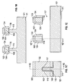
- Figure 1a depicts polysilicon and spacer formation on a fin in an embodiment.
- Figure 1a' illustrates a cross-sectional view of a tri-gate structure, which forms a portion of a circuit substrate.
- the structure includes a gate structure formed on substrate 111 and on a portion of body or fin 115.
- Substrate 111 can be bulk silicon or silicon-on-insulator (SOI).
- Fin 115 is in a different plane relative to substrate 111 and is situated perpendicular relative to the gate structure.
- Figure 1a includes a side view of fin 115 and includes two gate structures.
- Figure 1a is simplified and in reality there may be 1 such gate device or many more (e.g., 3, 4, 8) located along fin 115.
- substrate 111 can be composed of a single crystal semiconductor material, which can be, for example, silicon or germanium.
- Fin 115 may be composed of a semiconductor material such as silicon, germanium, SiGe, a III-V composition, combinations thereof, and the like.
- fin 115 includes buried section 101, which lies below the surface of the plane of the structure and is buried under oxide layer 105 and fin 115.
- fin 115, including buried section 101 may be formed by patterning and etching substrate 111 to define fin 115 as a portion (a non-planar portion) of the substrate and depositing dielectric material (e.g., oxide layer 105), on a surface of substrate 111 adjacent to fin 115 to define buried section 101.
- portions 101 and 111 are monolithic with one another. In other embodiments they may not be monolithic with each other and may include different materials, dopants, and the like.
- the gate structure mentioned above includes layers or portions 102, 103, 104, 116.
- Layer 116 can be a dielectric material, such as silicon dioxide (SiO 2 ), silicon nitride (Si 3 N 4 ), oxynitride (SiO y N x ) and the like.
- layer 116 can be a high dielectric constant (high-k) dielectric material, such as hafnium oxide (HfO 2 ).
- layer 116 can be a dielectric film with a metal at the top surface.
- Layer 102 can be a polycrystalline semiconductor material, such as polycrystalline silicon (polysilicon) or polysilicon germanium (poly-SiGe) or a metal material, such as titanium nitride.
- Layer 103 sometimes referred to as a "hard mask,” can be a non-conductive material, such as silicon dioxide, silicon nitride and the like.
- Portion 104 may include oxide spacers used in forming layers 102, 103, and/or 116.
- the embodiment of Figure 1 provides a form from which selective etching can be performed to build nano-scale dielectric structures embedded in ultra scaled devices (e.g., CMOS devices), such as devices scaled at 45, 32, 22, 14, 10 nm scales and like. More specifically, an embodiment concerns selective etching of a structure (e.g., fin), such as a buried structure, to form a void with the shape of the original structure. This void then functions as a mold. Flowable dielectric material fills the void to form the same shape as the original structure/mold.
- a structure e.g., fin
- Flowable dielectric material fills the void to form the same shape as the original structure/mold.
- Post-processing may then occur (e.g., oxidation build up and annealing under various conditions including environments containing O 2 , N 2 , H 2 , He, or various plasma treatments) to harden or covert or generally process the dielectric in the void.
- the resulting product has the same or nearly the same shape as the original structure but consists of different material than the original structure (e.g., dielectric instead of silicon).
- Embodiments of the method can provide a way to form an isolation layer in CMOS devices (i.e., the formed dielectric provides isolation).
- the middle gate structure may be converted to a dielectric isolation layer or device providing some isolation between the other two gate devices, which may become fully functioning tri-gate transistors.
- the molded dielectric can be utilized to fabricate dielectric nanostructures which can be used for passive components such as capacitors and inductors (both of which require dielectric isolation in some embodiments).
- the molded dielectric may be molded between two capacitive plates of a capacitor (e.g., a MIM capacitor) or within a coiled interconnect or line structure of an inductor.
- a capacitor e.g., a MIM capacitor
- MEMS microelectromechanical systems
- RF radiofrequency
- Figures 1b and 1c begin the transformation of the apparatus of Figure 1 a into a nano-scale dielectric structure.
- Figures 1b and 1c depict selective undercut etching partially completed ( Figure 1b ) and fully completed ( Figure 1c ).
- the etch may be selective to the materials of fin 115 (i.e., selective etching processes are those in which one material is etched rapidly while the other is etched very slowly or not etched at all) and/or may be a timed etch as well.
- the selective etch removes some or all of fin 115 leaving void 117 as a result.
- a portion of the original fin 115 remains with a void 117 where another portion of the fin used to be.
- Figure 1d shows the mold having been filled with flowable oxide 125, such as SiON, although silicon oxide, silicon nitride, silicon carbide, and the like are also possible flowable dielectrics in other embodiments.
- Figure 1e shows the apparatus after excess oxide 125 is removed by polishing (e.g., CMP).
- Figure 1f shows the apparatus after selective etching of layers 116, 102, 103 using etch specific chemistries corresponding to the materials of layers 116, 102, 103 using selective etch chemistries known to those of skill in the art.
- dielectric 125 is directly above the remainder of fin 115 (and/or the hidden portion 101).
- a buried structure e.g., fin 115
- dielectric 125 may include gate structures that were not etched away with the shape of the original fin structure.
- a source and drain may be located on either side of a still present gate structure to form a non-planar transistor.
- one or more of the gate structures of, for example, Figure 1e may be retained.
- portion 125 may be smaller and portion 115 may be larger than that shown in Figure 1e' .
- the etch of 115 may have been less severe.
- a source and drain may be located on either side of the gate to form a non-planar transistor.
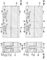
- Figure 2a includes a scanning electron microscope (SEM) image of a fin structure taken from a perspective analogous to Figure 1f' .
- the structure includes a fin portion 225, which includes SiON, based or formed on a fin portion 215, which includes silicon, all over substrate 201.
- Axis A shows how the sidewalls of portions 225, 215 are collinear illustrating how portion 225 was molded into the form previously made by upper portions of the original fin.
- Figure 2b includes a SEM image of a fin structure taken from a perspective analogous to Figure 1f .
- the structure includes a fin portion 225, which includes SiON, based on a fin portion 215, which includes silicon.
- Layer 202 includes polysilicon of a gate structure.
- Figure 3a depicts polysilicon and spacer formation in an embodiment.
- Figure 3a' illustrates a cross-sectional view of a tri-gate structure which forms a portion of a circuit substrate.
- the structure includes a gate structure formed on substrate 301 and on a portion of fin 315.
- Substrate 301 can be bulk silicon or SOI.
- Fin 315 is in a different plane relative to substrate 301 and is situated perpendicular relative to the gate structure.
- Figure 3a includes a side view of fin 315 and includes two gate structures.
- Figure 3a is simplified and in reality there may be 1 such gate device or many more (e.g., 3, 4, 8) located along fin 315.
- substrate 301 can be composed of a single crystal semiconductor material, which can be, for example, silicon or germanium and the like.
- Fin 315 may be composed of a semiconductor material such as silicon 314 on SiGe 313, and the like.
- fin 315 may be formed by patterning and etching substrate 301 to define fin 315 as a portion (a non-planar portion) of the substrate.
- Layer 314 may be grown epitaxially on layer 313 in some embodiments or may be formed via layer transfer and the like in other embodiments.
- the gate structure of Figure 3a can include layers or portions 302, 303, 304, 316.
- Layer 316 can be a dielectric material, such as SiO 2 , Si 3 N 4 , SiO y N x and the like. In some embodiments, layer 316 can be a high-k dielectric material, such as HfO 2 . Alternately, layer 316 can be a dielectric film with a metal at the top surface.
- Layer 302 can be a polycrystalline semiconductor material, such as polysilicon or poly-SiGe or a metal material, such as titanium nitride.
- Layer 303 sometimes referred to as a "hard mask,” can be a non-conductive material, such as silicon dioxide, silicon nitride and the like.
- Portion 304 may include oxide spacers used in forming layers 302, 303, and/or 316.
- Figure 3a provides a form from which selective etching can be performed to build nano-scale dielectric structures embedded in ultra scaled CMOS devices.
- Figure 3b begins the transformation of the apparatus of Figure 3a into a nano-scale dielectric structure.
- Figure 3b depicts selective undercut etching of SiGe 313 to form void 317. The selective etch removes some or all of the SiGe 313 portion of fin 315 leaving void 317 as a result. Void 317 will serve as a mold as seen below.
- Figure 3c shows the void/mold 317 having been filled with flowable oxide 325, such as SiON. While not shown, excess oxide 325 may be removed by polishing (e.g., CMP).
- polishing e.g., CMP
- the gate structure is maintained and there is no selective etching of layers 316, 302, 303. Thus, at this point dielectric 325 is directly above the remainder of fin portion 114.
- a buried structure e.g., fin portion 313
- CMOS transistor devices 305, 305' may each benefit from isolation dielectric 325 above portion 303 and isolation dielectric 325 below fin portion 314. This may promote less leakage current and/or resistive-capacitive (RC) delay performance and more efficient device operation overall.
- a source and drain may be formed on either side of gate structures 305, 305' to form non-planar transistors capable of full switching function.
- Embodiments described herein provide a nano-scale dielectric structure for highly scaled logic devices that utilize forms, such as fins, that can be etched to form molds that can be filled fully or partially with dielectric. This provides, for example, novel isolation for logic devices and may also enable novel passive components as described above.
- Block 401 includes forming a fin on a substrate, the fin including first and second portions that are collinear with one another and each intersect a vertical axis of the fin.
- Block 403 includes etching at least some of at least one of the first and second portions to form a void where the etching has occurred.
- Block 404 includes using the void as a mold to deposit flowable dielectric, in liquid form using a casting technique, within the void to contour the deposited dielectric to the contours of the void. This may yield, in some embodiments, a dielectric having been molded to include the same contour and dimensions as the original fin portion that was etched away. In an embodiment the sidewalls of the dielectric and remaining fin are collinear.
- Block 402 can optionally include forming a gate on the fin.
- terms designating relative vertical position refer to a situation where a device side (or active surface) of a substrate or integrated circuit is the "top” surface of that substrate; the substrate may actually be in any orientation so that a "top” side of a substrate may be lower than the “bottom” side in a standard terrestrial frame of reference and still fall within the meaning of the term “top.”
- the term “on” as used herein does not indicate that a first layer “on” a second layer is directly on and in immediate contact with the second layer unless such is specifically stated; there may be a third layer or other structure between the first layer and the second layer on the first layer.
- the embodiments of a device or article described herein can be manufactured, used, or shipped in a number of positions and orientations.
Landscapes
- Insulated Gate Type Field-Effect Transistor (AREA)
- Chemical & Material Sciences (AREA)
- Engineering & Computer Science (AREA)
- Materials Engineering (AREA)
- Nanotechnology (AREA)
- Moulds For Moulding Plastics Or The Like (AREA)
- Metal-Oxide And Bipolar Metal-Oxide Semiconductor Integrated Circuits (AREA)
Claims (5)
- Vorrichtung, umfassend:eine Lamelle (315), die einen Bodenanteil (325) und einen Deckanteil einschließt, die jeweils eine vertikale Achse der Lamelle schneiden;eine Gatestruktur, die sich oben auf der Lamelle (315) befindet und den Deckanteil (314) der Lamelle (315) an ersten und zweiten Seitenwänden und einer Deckfläche umgibt; undwobei (a) der Bodenanteil (325) ein fließfähiges Dielektrikum einschließt; (b) der Deckanteil (314) ein Halbleitermaterial, jedoch kein Dielektrikum einschließt, und dadurch gekennzeichnet, dass das fließfähige Dielektrikum die Seitenwände der Lamelle (315) und die Seitenwände und Deckfläche der Gatestruktur umgibt.
- Vorrichtung nach Anspruch 1, wobei das Halbleitermaterial ausgewählt ist aus der Gruppe umfassend Silicium, Germanium, SiGe, ein Element der Gruppe III und ein Element der Gruppe V.
- Vorrichtung nach Anspruch 1, wobei sich der Deckanteil (314) direkt oberhalb und in direktem Kontakt mit dem Bodenanteil (325) befindet.
- Verfahren, umfassend:Bilden einer Lamelle (315) auf einem Substrat (301), wobei die Lamelle (315) Deck- und Bodenanteile (314, 325) einschließt, die jeweils eine vertikale Achse der Lamelle (315) schneiden;Bilden eines Gates auf der Lamelle (315);wobei Ätzen von mindestens etwas von dem Bodenanteil (325), um einen Hohlraum zu bilden, Unterschnittätzen des Deckanteils (314) einschließt, während sich der Deckanteil (314) direkt unter dem Gate befindet;Ätzen von mindestens etwas von dem Bodenanteil (325), um dort einen Hohlraum zu bilden, wo das Ätzen stattgefunden hat;Verwenden des Hohlraums als Form, um fließfähiges Dielektrikum innerhalb des Hohlraums abzusetzen, um das abgeschiedene Dielektrikum mit den Konturen des Hohlraums zu konturieren;dadurch gekennzeichnet, dassdas fließfähige Dielektrikum die Seitenwände der Lamelle (315) und die Seitenwände und Deckfläche der Gatestruktur umgibt.
- Verfahren nach Anspruch 4, wobei:das fließfähige Dielektrikum ausgewählt ist aus der Gruppe umfassend Siliciumoxid, Siliciumdioxid, Siliciumnitrid, Oxynitrid (SiOyNx) und Siliciumcarbid;Ätzen von mindestens etwas von dem Bodenanteil, um einen Hohlraum zu bilden, selektives Ätzen des Bodenanteils mit einer Ätzchemie einschließt, die ausgelegt ist, um selektiv mindestens eines von dem Silicium, Germanium, einem Element der Gruppe III und einem Element der Gruppe V zu ätzen; undwobei das Verfahren des Weiteren Abscheiden des fließfähigen Dielektrikums in flüssiger Form unter Verwendung eines Gießprozesses umfasst.
Applications Claiming Priority (2)
| Application Number | Priority Date | Filing Date | Title |
|---|---|---|---|
| US14/138,254 US9882053B2 (en) | 2013-12-23 | 2013-12-23 | Molded dielectric fin-based nanostructure |
| PCT/IB2015/000218 WO2015097684A2 (en) | 2013-12-23 | 2015-02-23 | Molded dielectric nanostructure |
Publications (3)
| Publication Number | Publication Date |
|---|---|
| EP3087596A2 EP3087596A2 (de) | 2016-11-02 |
| EP3087596A4 EP3087596A4 (de) | 2017-07-19 |
| EP3087596B1 true EP3087596B1 (de) | 2019-12-11 |
Family
ID=53400987
Family Applications (1)
| Application Number | Title | Priority Date | Filing Date |
|---|---|---|---|
| EP15731235.6A Active EP3087596B1 (de) | 2013-12-23 | 2015-02-23 | Geformte dielektrische nanostruktur |
Country Status (6)
| Country | Link |
|---|---|
| US (1) | US9882053B2 (de) |
| EP (1) | EP3087596B1 (de) |
| KR (1) | KR102308910B1 (de) |
| CN (1) | CN106068556B (de) |
| TW (1) | TWI562274B (de) |
| WO (1) | WO2015097684A2 (de) |
Families Citing this family (4)
| Publication number | Priority date | Publication date | Assignee | Title |
|---|---|---|---|---|
| US11888034B2 (en) * | 2019-06-07 | 2024-01-30 | Intel Corporation | Transistors with metal chalcogenide channel materials |
| US11777029B2 (en) | 2019-06-27 | 2023-10-03 | Intel Corporation | Vertical transistors for ultra-dense logic and memory applications |
| US11171243B2 (en) | 2019-06-27 | 2021-11-09 | Intel Corporation | Transistor structures with a metal oxide contact buffer |
| US12266720B2 (en) | 2020-12-21 | 2025-04-01 | Intel Corporation | Transistors with monocrystalline metal chalcogenide channel materials |
Family Cites Families (15)
| Publication number | Priority date | Publication date | Assignee | Title |
|---|---|---|---|---|
| US7494862B2 (en) | 2006-09-29 | 2009-02-24 | Intel Corporation | Methods for uniform doping of non-planar transistor structures |
| US7666737B2 (en) * | 2006-12-18 | 2010-02-23 | Taiwan Semiconductor Manufacturing Co., Ltd. | Method of forming a metal-insulator-metal capacitor |
| US8912602B2 (en) | 2009-04-14 | 2014-12-16 | Taiwan Semiconductor Manufacturing Company, Ltd. | FinFETs and methods for forming the same |
| US8440517B2 (en) * | 2010-10-13 | 2013-05-14 | Taiwan Semiconductor Manufacturing Company, Ltd. | FinFET and method of fabricating the same |
| US20110140229A1 (en) | 2009-12-16 | 2011-06-16 | Willy Rachmady | Techniques for forming shallow trench isolation |
| CN102117829B (zh) | 2009-12-30 | 2012-11-21 | 中国科学院微电子研究所 | 鳍式晶体管结构及其制作方法 |
| US8354719B2 (en) | 2010-02-18 | 2013-01-15 | GlobalFoundries, Inc. | Finned semiconductor device with oxygen diffusion barrier regions, and related fabrication methods |
| US8420476B2 (en) | 2010-05-27 | 2013-04-16 | International Business Machines Corporation | Integrated circuit with finFETs and MIM fin capacitor |
| US8492235B2 (en) | 2010-12-29 | 2013-07-23 | Globalfoundries Singapore Pte. Ltd. | FinFET with stressors |
| JP2012235059A (ja) | 2011-05-09 | 2012-11-29 | Toshiba Corp | 半導体装置および半導体装置の製造方法 |
| US8541286B2 (en) | 2012-02-17 | 2013-09-24 | GlobalFoundries, Inc. | Methods for fabricating integrated circuits |
| US8853037B2 (en) * | 2012-03-14 | 2014-10-07 | GlobalFoundries, Inc. | Methods for fabricating integrated circuits |
| US8872284B2 (en) * | 2012-03-20 | 2014-10-28 | Taiwan Semiconductor Manufacturing Company, Ltd. | FinFET with metal gate stressor |
| US20130270638A1 (en) * | 2012-04-13 | 2013-10-17 | International Business Machines Corporation | Strained soi finfet on epitaxially grown box |
| US9006077B2 (en) * | 2013-08-21 | 2015-04-14 | GlobalFoundries, Inc. | Gate length independent silicon-on-nothing (SON) scheme for bulk FinFETs |
-
2013
- 2013-12-23 US US14/138,254 patent/US9882053B2/en not_active Expired - Fee Related
-
2014
- 2014-11-19 TW TW103140071A patent/TWI562274B/zh active
-
2015
- 2015-02-23 WO PCT/IB2015/000218 patent/WO2015097684A2/en not_active Ceased
- 2015-02-23 CN CN201580002713.4A patent/CN106068556B/zh not_active Expired - Fee Related
- 2015-02-23 KR KR1020167013547A patent/KR102308910B1/ko active Active
- 2015-02-23 EP EP15731235.6A patent/EP3087596B1/de active Active
Non-Patent Citations (1)
| Title |
|---|
| None * |
Also Published As
| Publication number | Publication date |
|---|---|
| CN106068556B (zh) | 2021-06-18 |
| WO2015097684A2 (en) | 2015-07-02 |
| KR20170112995A (ko) | 2017-10-12 |
| WO2015097684A3 (en) | 2015-10-08 |
| EP3087596A4 (de) | 2017-07-19 |
| TW201541554A (zh) | 2015-11-01 |
| US20150179786A1 (en) | 2015-06-25 |
| WO2015097684A8 (en) | 2016-04-07 |
| US9882053B2 (en) | 2018-01-30 |
| KR102308910B1 (ko) | 2021-10-05 |
| CN106068556A (zh) | 2016-11-02 |
| EP3087596A2 (de) | 2016-11-02 |
| TWI562274B (en) | 2016-12-11 |
Similar Documents
| Publication | Publication Date | Title |
|---|---|---|
| US11621323B2 (en) | Fill fins for semiconductor devices | |
| US11515304B2 (en) | Integrated circuit devices with non-collapsed fins and methods of treating the fins to prevent fin collapse | |
| US9954062B2 (en) | Stacked planar double-gate lamellar field-effect transistor | |
| US20190172755A1 (en) | Method for incorporating multiple channel materials in a complimentary field effective transistor (cfet) device | |
| US10510875B2 (en) | Source and drain structure with reduced contact resistance and enhanced mobility | |
| KR101656952B1 (ko) | Fin 피처의 구조물 및 그 제조 방법 | |
| US9117875B2 (en) | Methods of forming isolated germanium-containing fins for a FinFET semiconductor device | |
| US20160079125A1 (en) | Semiconductor devices and methods of manufacturing the same | |
| US8889500B1 (en) | Methods of forming stressed fin channel structures for FinFET semiconductor devices | |
| CN109326645B (zh) | 半导体器件及其制造方法 | |
| TW201724213A (zh) | 具有增加接觸面積的半導體裝置接觸 | |
| KR102639002B1 (ko) | 강유전체 메모리를 포함하는 반도체 디바이스들 및 그 형성 방법들 | |
| EP3087596B1 (de) | Geformte dielektrische nanostruktur | |
| TW202406149A (zh) | 半導體裝置及其製造方法 | |
| US20180108732A1 (en) | Notched fin structures and methods of manufacture | |
| US9620589B2 (en) | Integrated circuits and methods of fabrication thereof | |
| KR102815318B1 (ko) | 고성능 다차원 소자 및 로직 집적 | |
| US20230068854A1 (en) | Method of making a plurality of 3d semiconductor devices with enhanced mobility and conductivity | |
| US20250022746A1 (en) | Isolation between device areas | |
| US20250169178A1 (en) | 3d fet devices and methods for manufacturing the same | |
| TWI832133B (zh) | 半導體元件及方法 | |
| JP2025521393A (ja) | 誘電体分離を備えるゲートオールアラウンド・デバイスのためのcppに依存しないソース-ドレイン・コンタクト形成 | |
| CN119008627A (zh) | 具有可调沟道和内侧壁间隔物的纳米片结构 |
Legal Events
| Date | Code | Title | Description |
|---|---|---|---|
| PUAI | Public reference made under article 153(3) epc to a published international application that has entered the european phase |
Free format text: ORIGINAL CODE: 0009012 |
|
| 17P | Request for examination filed |
Effective date: 20160602 |
|
| AK | Designated contracting states |
Kind code of ref document: A2 Designated state(s): AL AT BE BG CH CY CZ DE DK EE ES FI FR GB GR HR HU IE IS IT LI LT LU LV MC MK MT NL NO PL PT RO RS SE SI SK SM TR |
|
| AX | Request for extension of the european patent |
Extension state: BA ME |
|
| DAX | Request for extension of the european patent (deleted) | ||
| A4 | Supplementary search report drawn up and despatched |
Effective date: 20170621 |
|
| RIC1 | Information provided on ipc code assigned before grant |
Ipc: H01L 21/762 20060101AFI20170615BHEP Ipc: H01L 21/336 20060101ALI20170615BHEP Ipc: H01L 29/66 20060101ALI20170615BHEP Ipc: H01L 29/78 20060101ALI20170615BHEP |
|
| REG | Reference to a national code |
Ref country code: DE Ref legal event code: R079 Ref document number: 602015043429 Country of ref document: DE Free format text: PREVIOUS MAIN CLASS: H01L0021762000 Ipc: H01L0021560000 |
|
| RIC1 | Information provided on ipc code assigned before grant |
Ipc: H01L 29/66 20060101ALI20190502BHEP Ipc: H01L 29/78 20060101ALI20190502BHEP Ipc: H01L 21/56 20060101AFI20190502BHEP |
|
| GRAP | Despatch of communication of intention to grant a patent |
Free format text: ORIGINAL CODE: EPIDOSNIGR1 |
|
| STAA | Information on the status of an ep patent application or granted ep patent |
Free format text: STATUS: GRANT OF PATENT IS INTENDED |
|
| INTG | Intention to grant announced |
Effective date: 20190701 |
|
| GRAS | Grant fee paid |
Free format text: ORIGINAL CODE: EPIDOSNIGR3 |
|
| GRAA | (expected) grant |
Free format text: ORIGINAL CODE: 0009210 |
|
| STAA | Information on the status of an ep patent application or granted ep patent |
Free format text: STATUS: THE PATENT HAS BEEN GRANTED |
|
| AK | Designated contracting states |
Kind code of ref document: B1 Designated state(s): AL AT BE BG CH CY CZ DE DK EE ES FI FR GB GR HR HU IE IS IT LI LT LU LV MC MK MT NL NO PL PT RO RS SE SI SK SM TR |
|
| REG | Reference to a national code |
Ref country code: GB Ref legal event code: FG4D |
|
| REG | Reference to a national code |
Ref country code: CH Ref legal event code: EP |
|
| REG | Reference to a national code |
Ref country code: AT Ref legal event code: REF Ref document number: 1213039 Country of ref document: AT Kind code of ref document: T Effective date: 20191215 |
|
| REG | Reference to a national code |
Ref country code: DE Ref legal event code: R096 Ref document number: 602015043429 Country of ref document: DE |
|
| REG | Reference to a national code |
Ref country code: IE Ref legal event code: FG4D |
|
| REG | Reference to a national code |
Ref country code: NL Ref legal event code: FP |
|
| REG | Reference to a national code |
Ref country code: LT Ref legal event code: MG4D |
|
| PG25 | Lapsed in a contracting state [announced via postgrant information from national office to epo] |
Ref country code: LV Free format text: LAPSE BECAUSE OF FAILURE TO SUBMIT A TRANSLATION OF THE DESCRIPTION OR TO PAY THE FEE WITHIN THE PRESCRIBED TIME-LIMIT Effective date: 20191211 Ref country code: SE Free format text: LAPSE BECAUSE OF FAILURE TO SUBMIT A TRANSLATION OF THE DESCRIPTION OR TO PAY THE FEE WITHIN THE PRESCRIBED TIME-LIMIT Effective date: 20191211 Ref country code: BG Free format text: LAPSE BECAUSE OF FAILURE TO SUBMIT A TRANSLATION OF THE DESCRIPTION OR TO PAY THE FEE WITHIN THE PRESCRIBED TIME-LIMIT Effective date: 20200311 Ref country code: FI Free format text: LAPSE BECAUSE OF FAILURE TO SUBMIT A TRANSLATION OF THE DESCRIPTION OR TO PAY THE FEE WITHIN THE PRESCRIBED TIME-LIMIT Effective date: 20191211 Ref country code: NO Free format text: LAPSE BECAUSE OF FAILURE TO SUBMIT A TRANSLATION OF THE DESCRIPTION OR TO PAY THE FEE WITHIN THE PRESCRIBED TIME-LIMIT Effective date: 20200311 Ref country code: GR Free format text: LAPSE BECAUSE OF FAILURE TO SUBMIT A TRANSLATION OF THE DESCRIPTION OR TO PAY THE FEE WITHIN THE PRESCRIBED TIME-LIMIT Effective date: 20200312 Ref country code: LT Free format text: LAPSE BECAUSE OF FAILURE TO SUBMIT A TRANSLATION OF THE DESCRIPTION OR TO PAY THE FEE WITHIN THE PRESCRIBED TIME-LIMIT Effective date: 20191211 |
|
| PG25 | Lapsed in a contracting state [announced via postgrant information from national office to epo] |
Ref country code: RS Free format text: LAPSE BECAUSE OF FAILURE TO SUBMIT A TRANSLATION OF THE DESCRIPTION OR TO PAY THE FEE WITHIN THE PRESCRIBED TIME-LIMIT Effective date: 20191211 Ref country code: HR Free format text: LAPSE BECAUSE OF FAILURE TO SUBMIT A TRANSLATION OF THE DESCRIPTION OR TO PAY THE FEE WITHIN THE PRESCRIBED TIME-LIMIT Effective date: 20191211 |
|
| PG25 | Lapsed in a contracting state [announced via postgrant information from national office to epo] |
Ref country code: AL Free format text: LAPSE BECAUSE OF FAILURE TO SUBMIT A TRANSLATION OF THE DESCRIPTION OR TO PAY THE FEE WITHIN THE PRESCRIBED TIME-LIMIT Effective date: 20191211 |
|
| PG25 | Lapsed in a contracting state [announced via postgrant information from national office to epo] |
Ref country code: EE Free format text: LAPSE BECAUSE OF FAILURE TO SUBMIT A TRANSLATION OF THE DESCRIPTION OR TO PAY THE FEE WITHIN THE PRESCRIBED TIME-LIMIT Effective date: 20191211 Ref country code: RO Free format text: LAPSE BECAUSE OF FAILURE TO SUBMIT A TRANSLATION OF THE DESCRIPTION OR TO PAY THE FEE WITHIN THE PRESCRIBED TIME-LIMIT Effective date: 20191211 Ref country code: CZ Free format text: LAPSE BECAUSE OF FAILURE TO SUBMIT A TRANSLATION OF THE DESCRIPTION OR TO PAY THE FEE WITHIN THE PRESCRIBED TIME-LIMIT Effective date: 20191211 Ref country code: ES Free format text: LAPSE BECAUSE OF FAILURE TO SUBMIT A TRANSLATION OF THE DESCRIPTION OR TO PAY THE FEE WITHIN THE PRESCRIBED TIME-LIMIT Effective date: 20191211 Ref country code: PT Free format text: LAPSE BECAUSE OF FAILURE TO SUBMIT A TRANSLATION OF THE DESCRIPTION OR TO PAY THE FEE WITHIN THE PRESCRIBED TIME-LIMIT Effective date: 20200506 |
|
| PG25 | Lapsed in a contracting state [announced via postgrant information from national office to epo] |
Ref country code: IS Free format text: LAPSE BECAUSE OF FAILURE TO SUBMIT A TRANSLATION OF THE DESCRIPTION OR TO PAY THE FEE WITHIN THE PRESCRIBED TIME-LIMIT Effective date: 20200411 Ref country code: SM Free format text: LAPSE BECAUSE OF FAILURE TO SUBMIT A TRANSLATION OF THE DESCRIPTION OR TO PAY THE FEE WITHIN THE PRESCRIBED TIME-LIMIT Effective date: 20191211 Ref country code: SK Free format text: LAPSE BECAUSE OF FAILURE TO SUBMIT A TRANSLATION OF THE DESCRIPTION OR TO PAY THE FEE WITHIN THE PRESCRIBED TIME-LIMIT Effective date: 20191211 |
|
| REG | Reference to a national code |
Ref country code: DE Ref legal event code: R097 Ref document number: 602015043429 Country of ref document: DE |
|
| REG | Reference to a national code |
Ref country code: CH Ref legal event code: PL |
|
| REG | Reference to a national code |
Ref country code: AT Ref legal event code: MK05 Ref document number: 1213039 Country of ref document: AT Kind code of ref document: T Effective date: 20191211 |
|
| PLBE | No opposition filed within time limit |
Free format text: ORIGINAL CODE: 0009261 |
|
| STAA | Information on the status of an ep patent application or granted ep patent |
Free format text: STATUS: NO OPPOSITION FILED WITHIN TIME LIMIT |
|
| REG | Reference to a national code |
Ref country code: BE Ref legal event code: MM Effective date: 20200229 |
|
| PG25 | Lapsed in a contracting state [announced via postgrant information from national office to epo] |
Ref country code: MC Free format text: LAPSE BECAUSE OF FAILURE TO SUBMIT A TRANSLATION OF THE DESCRIPTION OR TO PAY THE FEE WITHIN THE PRESCRIBED TIME-LIMIT Effective date: 20191211 Ref country code: DK Free format text: LAPSE BECAUSE OF FAILURE TO SUBMIT A TRANSLATION OF THE DESCRIPTION OR TO PAY THE FEE WITHIN THE PRESCRIBED TIME-LIMIT Effective date: 20191211 Ref country code: LU Free format text: LAPSE BECAUSE OF NON-PAYMENT OF DUE FEES Effective date: 20200223 |
|
| 26N | No opposition filed |
Effective date: 20200914 |
|
| PG25 | Lapsed in a contracting state [announced via postgrant information from national office to epo] |
Ref country code: CH Free format text: LAPSE BECAUSE OF NON-PAYMENT OF DUE FEES Effective date: 20200229 Ref country code: SI Free format text: LAPSE BECAUSE OF FAILURE TO SUBMIT A TRANSLATION OF THE DESCRIPTION OR TO PAY THE FEE WITHIN THE PRESCRIBED TIME-LIMIT Effective date: 20191211 Ref country code: AT Free format text: LAPSE BECAUSE OF FAILURE TO SUBMIT A TRANSLATION OF THE DESCRIPTION OR TO PAY THE FEE WITHIN THE PRESCRIBED TIME-LIMIT Effective date: 20191211 Ref country code: LI Free format text: LAPSE BECAUSE OF NON-PAYMENT OF DUE FEES Effective date: 20200229 |
|
| PG25 | Lapsed in a contracting state [announced via postgrant information from national office to epo] |
Ref country code: IT Free format text: LAPSE BECAUSE OF FAILURE TO SUBMIT A TRANSLATION OF THE DESCRIPTION OR TO PAY THE FEE WITHIN THE PRESCRIBED TIME-LIMIT Effective date: 20191211 Ref country code: IE Free format text: LAPSE BECAUSE OF NON-PAYMENT OF DUE FEES Effective date: 20200223 |
|
| PG25 | Lapsed in a contracting state [announced via postgrant information from national office to epo] |
Ref country code: PL Free format text: LAPSE BECAUSE OF FAILURE TO SUBMIT A TRANSLATION OF THE DESCRIPTION OR TO PAY THE FEE WITHIN THE PRESCRIBED TIME-LIMIT Effective date: 20191211 Ref country code: BE Free format text: LAPSE BECAUSE OF NON-PAYMENT OF DUE FEES Effective date: 20200229 |
|
| PG25 | Lapsed in a contracting state [announced via postgrant information from national office to epo] |
Ref country code: TR Free format text: LAPSE BECAUSE OF FAILURE TO SUBMIT A TRANSLATION OF THE DESCRIPTION OR TO PAY THE FEE WITHIN THE PRESCRIBED TIME-LIMIT Effective date: 20191211 Ref country code: MT Free format text: LAPSE BECAUSE OF FAILURE TO SUBMIT A TRANSLATION OF THE DESCRIPTION OR TO PAY THE FEE WITHIN THE PRESCRIBED TIME-LIMIT Effective date: 20191211 Ref country code: CY Free format text: LAPSE BECAUSE OF FAILURE TO SUBMIT A TRANSLATION OF THE DESCRIPTION OR TO PAY THE FEE WITHIN THE PRESCRIBED TIME-LIMIT Effective date: 20191211 |
|
| PG25 | Lapsed in a contracting state [announced via postgrant information from national office to epo] |
Ref country code: MK Free format text: LAPSE BECAUSE OF FAILURE TO SUBMIT A TRANSLATION OF THE DESCRIPTION OR TO PAY THE FEE WITHIN THE PRESCRIBED TIME-LIMIT Effective date: 20191211 |
|
| P01 | Opt-out of the competence of the unified patent court (upc) registered |
Effective date: 20230518 |
|
| PGFP | Annual fee paid to national office [announced via postgrant information from national office to epo] |
Ref country code: GB Payment date: 20231207 Year of fee payment: 10 |
|
| PGFP | Annual fee paid to national office [announced via postgrant information from national office to epo] |
Ref country code: NL Payment date: 20231215 Year of fee payment: 10 Ref country code: FR Payment date: 20231212 Year of fee payment: 10 |
|
| REG | Reference to a national code |
Ref country code: NL Ref legal event code: MM Effective date: 20250301 |
|
| GBPC | Gb: european patent ceased through non-payment of renewal fee |
Effective date: 20250223 |
|
| PG25 | Lapsed in a contracting state [announced via postgrant information from national office to epo] |
Ref country code: NL Free format text: LAPSE BECAUSE OF NON-PAYMENT OF DUE FEES Effective date: 20250301 |
|
| REG | Reference to a national code |
Ref country code: DE Ref legal event code: R079 Ref document number: 602015043429 Country of ref document: DE Free format text: PREVIOUS MAIN CLASS: H01L0021560000 Ipc: H10W0074010000 |
|
| PG25 | Lapsed in a contracting state [announced via postgrant information from national office to epo] |
Ref country code: GB Free format text: LAPSE BECAUSE OF NON-PAYMENT OF DUE FEES Effective date: 20250223 |
|
| PG25 | Lapsed in a contracting state [announced via postgrant information from national office to epo] |
Ref country code: FR Free format text: LAPSE BECAUSE OF NON-PAYMENT OF DUE FEES Effective date: 20250228 |
|
| PGFP | Annual fee paid to national office [announced via postgrant information from national office to epo] |
Ref country code: DE Payment date: 20260102 Year of fee payment: 12 |