EP3087629B1 - Procédé de fabrication de couche semi-conductrice nanocristalline poreuse, couche semi-conductrice nanocristalline poreuse, utilisation de cette dernière, anode et batterie lithium-ion secondaire - Google Patents
Procédé de fabrication de couche semi-conductrice nanocristalline poreuse, couche semi-conductrice nanocristalline poreuse, utilisation de cette dernière, anode et batterie lithium-ion secondaire Download PDFInfo
- Publication number
- EP3087629B1 EP3087629B1 EP13814164.3A EP13814164A EP3087629B1 EP 3087629 B1 EP3087629 B1 EP 3087629B1 EP 13814164 A EP13814164 A EP 13814164A EP 3087629 B1 EP3087629 B1 EP 3087629B1
- Authority
- EP
- European Patent Office
- Prior art keywords
- metal
- layer
- semiconductor layer
- semiconductor
- substrate
- Prior art date
- Legal status (The legal status is an assumption and is not a legal conclusion. Google has not performed a legal analysis and makes no representation as to the accuracy of the status listed.)
- Not-in-force
Links
Images




Classifications
-
- H—ELECTRICITY
- H01—ELECTRIC ELEMENTS
- H01M—PROCESSES OR MEANS, e.g. BATTERIES, FOR THE DIRECT CONVERSION OF CHEMICAL ENERGY INTO ELECTRICAL ENERGY
- H01M4/00—Electrodes
- H01M4/02—Electrodes composed of, or comprising, active material
- H01M4/36—Selection of substances as active materials, active masses, active liquids
- H01M4/38—Selection of substances as active materials, active masses, active liquids of elements or alloys
- H01M4/386—Silicon or alloys based on silicon
-
- H—ELECTRICITY
- H01—ELECTRIC ELEMENTS
- H01M—PROCESSES OR MEANS, e.g. BATTERIES, FOR THE DIRECT CONVERSION OF CHEMICAL ENERGY INTO ELECTRICAL ENERGY
- H01M10/00—Secondary cells; Manufacture thereof
- H01M10/05—Accumulators with non-aqueous electrolyte
- H01M10/052—Li-accumulators
- H01M10/0525—Rocking-chair batteries, i.e. batteries with lithium insertion or intercalation in both electrodes; Lithium-ion batteries
-
- H—ELECTRICITY
- H01—ELECTRIC ELEMENTS
- H01M—PROCESSES OR MEANS, e.g. BATTERIES, FOR THE DIRECT CONVERSION OF CHEMICAL ENERGY INTO ELECTRICAL ENERGY
- H01M4/00—Electrodes
- H01M4/02—Electrodes composed of, or comprising, active material
- H01M4/04—Processes of manufacture in general
- H01M4/0402—Methods of deposition of the material
- H01M4/0404—Methods of deposition of the material by coating on electrode collectors
-
- H—ELECTRICITY
- H01—ELECTRIC ELEMENTS
- H01M—PROCESSES OR MEANS, e.g. BATTERIES, FOR THE DIRECT CONVERSION OF CHEMICAL ENERGY INTO ELECTRICAL ENERGY
- H01M4/00—Electrodes
- H01M4/02—Electrodes composed of, or comprising, active material
- H01M4/04—Processes of manufacture in general
- H01M4/0471—Processes of manufacture in general involving thermal treatment, e.g. firing, sintering, backing particulate active material, thermal decomposition, pyrolysis
-
- H—ELECTRICITY
- H01—ELECTRIC ELEMENTS
- H01M—PROCESSES OR MEANS, e.g. BATTERIES, FOR THE DIRECT CONVERSION OF CHEMICAL ENERGY INTO ELECTRICAL ENERGY
- H01M4/00—Electrodes
- H01M4/02—Electrodes composed of, or comprising, active material
- H01M4/13—Electrodes for accumulators with non-aqueous electrolyte, e.g. for lithium-accumulators; Processes of manufacture thereof
- H01M4/134—Electrodes based on metals, Si or alloys
-
- H—ELECTRICITY
- H01—ELECTRIC ELEMENTS
- H01M—PROCESSES OR MEANS, e.g. BATTERIES, FOR THE DIRECT CONVERSION OF CHEMICAL ENERGY INTO ELECTRICAL ENERGY
- H01M4/00—Electrodes
- H01M4/02—Electrodes composed of, or comprising, active material
- H01M4/13—Electrodes for accumulators with non-aqueous electrolyte, e.g. for lithium-accumulators; Processes of manufacture thereof
- H01M4/139—Processes of manufacture
- H01M4/1395—Processes of manufacture of electrodes based on metals, Si or alloys
-
- H—ELECTRICITY
- H01—ELECTRIC ELEMENTS
- H01M—PROCESSES OR MEANS, e.g. BATTERIES, FOR THE DIRECT CONVERSION OF CHEMICAL ENERGY INTO ELECTRICAL ENERGY
- H01M10/00—Secondary cells; Manufacture thereof
- H01M10/05—Accumulators with non-aqueous electrolyte
- H01M10/052—Li-accumulators
-
- H—ELECTRICITY
- H01—ELECTRIC ELEMENTS
- H01M—PROCESSES OR MEANS, e.g. BATTERIES, FOR THE DIRECT CONVERSION OF CHEMICAL ENERGY INTO ELECTRICAL ENERGY
- H01M4/00—Electrodes
- H01M4/02—Electrodes composed of, or comprising, active material
- H01M2004/021—Physical characteristics, e.g. porosity, surface area
-
- H—ELECTRICITY
- H10—SEMICONDUCTOR DEVICES; ELECTRIC SOLID-STATE DEVICES NOT OTHERWISE PROVIDED FOR
- H10P—GENERIC PROCESSES OR APPARATUS FOR THE MANUFACTURE OR TREATMENT OF DEVICES COVERED BY CLASS H10
- H10P14/00—Formation of materials, e.g. in the shape of layers or pillars
- H10P14/20—Formation of materials, e.g. in the shape of layers or pillars of semiconductor materials
- H10P14/34—Deposited materials, e.g. layers
- H10P14/3402—Deposited materials, e.g. layers characterised by the chemical composition
- H10P14/3404—Deposited materials, e.g. layers characterised by the chemical composition being Group IVA materials
- H10P14/3411—Silicon, silicon germanium or germanium
-
- H—ELECTRICITY
- H10—SEMICONDUCTOR DEVICES; ELECTRIC SOLID-STATE DEVICES NOT OTHERWISE PROVIDED FOR
- H10P—GENERIC PROCESSES OR APPARATUS FOR THE MANUFACTURE OR TREATMENT OF DEVICES COVERED BY CLASS H10
- H10P14/00—Formation of materials, e.g. in the shape of layers or pillars
- H10P14/20—Formation of materials, e.g. in the shape of layers or pillars of semiconductor materials
- H10P14/34—Deposited materials, e.g. layers
- H10P14/3451—Structure
- H10P14/3452—Microstructure
-
- Y—GENERAL TAGGING OF NEW TECHNOLOGICAL DEVELOPMENTS; GENERAL TAGGING OF CROSS-SECTIONAL TECHNOLOGIES SPANNING OVER SEVERAL SECTIONS OF THE IPC; TECHNICAL SUBJECTS COVERED BY FORMER USPC CROSS-REFERENCE ART COLLECTIONS [XRACs] AND DIGESTS
- Y02—TECHNOLOGIES OR APPLICATIONS FOR MITIGATION OR ADAPTATION AGAINST CLIMATE CHANGE
- Y02E—REDUCTION OF GREENHOUSE GAS [GHG] EMISSIONS, RELATED TO ENERGY GENERATION, TRANSMISSION OR DISTRIBUTION
- Y02E60/00—Enabling technologies; Technologies with a potential or indirect contribution to GHG emissions mitigation
- Y02E60/10—Energy storage using batteries
Definitions
- the present invention is directed to a method for producing a porous nanocrystalline semiconductor layer, a porous nanocrystalline semiconductor layer, a use thereof, an anode, and a secondary lithium-ion battery.
- Silicon has turned into one of the most promising materials for anodes for secondary lithium-ion batteries, such as high energy rechargeable Li-ion batteries.
- a huge expansion 300 to 400%) during alloying with Li may induce pulverization/delamination for micro-sized electrodes, as well as undesired accumulation of solid electrolyte interphase (SEI).
- SEI solid electrolyte interphase
- Li-ion batteries e.g. for applications in hybrid electric vehicles (HEV) and plug-in HEV (PHEV)
- high capacity electrodes are required.
- electrodes for small electronic equipment of high power needs and/or long operating times.
- silicon-based materials as typical alloy anodes are top candidates owing to the extremely high theoretical capacity of 4200 mAh/g, based on the formation of Li 22 Si 5 phase, exceeding that of the widely used graphite insertion anode (372 mAh/g) by more than a factor of 10.
- Si nanostructures such as nanowires and nanoparticles, or their composites (e.g. coated by carbon or conjugated polymer, alloying with inactive metal) with well-defined morphologies or ionic/electronic wiring networks have been exploited to address these problems ( Chan, C. K., Peng, H. L., Liu, G., Mcllwrath, K., Zhang, X. F., Huggins, R. A.
- CMC carboxymethyl cellulose
- PAA polyacrylic acid
- FEC fluoroethylene carbonate
- an alternative method is to reduce the amount of inactive components during electrode preparation.
- Si thin film architectures without the usage of binders and additional conductive substances have been reported, which show near theoretical capacity with good cyclability as long as the film thickness is below the critical cracking value of about 300 nm to prevent delamination or fracture of thin films from substrates during lithiation-driven volume expansion ( Ohara, S., Suzuki, J., Sekine, K. & Takamura, T.
- micro-sized Si thick films are required to achieve high area specific capacity, and still, most of methods previously focused on the fabrication of state-of-the-art nano-composites by using slurrying and pasting processes.
- the large-scale deposition of nano-architecture Si thick films, for instance having a thickness > 1 pm, without mixing with binder and conductive additives remains a significant challenge (Usui, H., Uchida, N. & Sakaguchi, H. Influence of order in stepwise electroless deposition on anode properties of thick-film electrodes consisting of Si particles coated with Ni and Cu. J Power Sources 196, 10244-10248 (2011 )).
- a porous silicon based material including porous crystalline elemental silicon formed by reducing silicon dioxide with a reducing metal in a heating process followed by acid etching is used to construct a negative electrode for lithium ion batteries.
- Alford et al. (Nanocrystalline Si formation in the a-Si/Al system on polyimide and silicon dioxide substrates, Thin Solid Films 516, 3940-3947 (2008 )) relates to the preparation of silicon films containing nanocrystallites and pores suitable for application in thin film transistors.
- an 800 nm layer of amorphous silicon (a-Si) and a 20 nm layer of Al are sequentially deposited on a substrate, so that the Al layer is on top of the a-Si layer.
- Thermal annealing results in the formation of a thin layer of silicon that contains Si pores and nanocrystallites, which are present in the top 200 nm of the sample, just beneath the Al layer.
- US 2013/189575 A1 discloses a porous silicon-based electrode material for use in lithium ion batteries comprising porous crystalline elemental silicon formed by reducing silicon dioxide using a reducing metal in a heating process, followed by acid etching.
- the porous silicon-based material formed has an average pore size in the range of 5 nm to 500 nm in diameter.
- US 2004/161369 A1 discloses metal-coated nanocrystalline porous silicon substrates usable in apparatus for Raman detection,
- the porous silicon is produced by etching a silicon substrate with dilute hydrofluoric acid in an electrochemical cell, whereby a pore size of 2 nm to 200 nm can be achieved.
- Object of the invention is to provide a method for producing a porous nanocrystalline semiconductor layer and a porous nanocrystalline semiconductor layer obtained thereby.
- This object is achieved by a method for producing a porous nanocrystalline semiconductor layer according to claim 1, a porous nanocrystalline semiconductor layer according to claim 8, a use of the porous nanocrystalline semiconductor layer according to claim 12, an anode according to claim 13, and a secondary lithium-ion battery according to claim 14.
- a method for producing a porous nanocrystalline semiconductor layer including: a) providing a substrate having a substrate surface; b) coating a semiconductor layer on the substrate surface; c) coating a metal containing layer on the semiconductor layer; d) heat treating the semiconductor layer and the metal containing layer at a temperature and for a time period such that the semiconductor layer and the metal containing layer partially interdiffuse and the semiconductor is at least partially crystallized; and e) at least partially removing the metal.
- a porous nanocrystalline semiconductor layer is provided, obtainable or obtained by a method of any of the preceding claims, wherein the semiconductor layer is provided on a substrate and includes an outer surface and macropores extending from the outer surface of the semiconductor layer towards the substrate, and wherein the macropores have a depth of 600 to 2100 nm.
- a third embodiment provides a use of a porous nanocrystalline semiconductor layer according to the first embodiment in an electrode and/or in an anode for an energy storage device or for a secondary lithium-ion battery.
- a fourth embodiment is directed to an anode for a secondary lithium-ion battery, including the porous nanocrystalline semiconductor layer according to the second embodiment.
- a secondary lithium-ion battery including an anode according to the fourth embodiment is provided.
- embodiments of the method according to the invention allow for a metal-induced crystallization of partially miscible or immiscible metal/semiconductor systems, e.g. Si/Al bilayers, to prepare semiconductur films having a thickness of e.g. > 300 nm, in particular ⁇ 1 pm, and including a high density of macropores.
- This method furthermore brings about low temperature crystallization of an initial amorphous semiconductor, including a post-deposition pore-creating.
- a coating of metal oxide, preferably conformal to the semiconductor layer and/or ion-conductive, to enhance the Li transport kinetics of bulk and interface is provided. Both highly satisfactory capacity retention (e.g.
- anodes according to embodiments of the invention, which include the nanocrystalline semiconductor layers of embodiments.
- the method of embodiments of the invention can be used to prepare porous nanocrystalline semiconductor layers with well-defined nanostructures, but free of extra binder and conductive additives. Thereby, a much higher area specific capacity of an anode can be achieved than by methods providing inactive-component contained slurry samples and thin film samples.
- the method can be performed using linear processing tools and/or continuous substrates.
- the term "porous" or "pore” may be understood as at least including macropores.
- macropores may be pores having a pore size, i.e. at least a width and/or a depth, of more than about 50 nm.
- the semiconductor layer of embodiments may also include mesopores and/or micropores, i.e. pores equal to or smaller than about 50 nm.
- mesopores and/or micropores i.e. pores equal to or smaller than about 50 nm.
- layer and film are used synonymously.
- nanocrystalline may be understood as at least including crystalline zones having a width of at least about 1 nm, preferably at least about 5 nm, more preferably of at least about 10 nm, for instance of about 1 nm to 30 nm.
- the nanocrystalline zones may be as large as the surface structures 106, e.g. each of the surface structures may be single crystalline.
- the crystalline nature may for instance be derived from XRD (X-Ray Diffraction).
- a method for producing a porous nanocrystalline semiconductor layer including: a) providing a substrate having a substrate surface; b) coating a semiconductor layer on the substrate surface; c) coating a metal containing layer on the semiconductor layer; d) heat treating the semiconductor layer and the metal containing layer at a temperature and for a time period such that the semiconductor layer and the metal containing layer partially interdiffuse and the semiconductor is at least partially crystallized; and e) at least partially removing the metal.
- the metal may be at least partially removed from the heat treated coated substrate. Further, in step e) the metal may be at least partially removed by etching the heat treated coated substrate.
- Embodiments of the invention surprisingly provide a nano-engineering method for forming a porous semiconductor layer, based on incomplete layer exchange and phase separation between metal and semiconductor phases, based on metal-induced crystallization and layer exchange in semiconductor/metal bilayers.
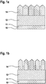
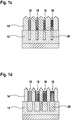
- Fig. 1d the metal partially diffuses downwards into the original amorphous semiconductor, leading to secondary crystallization of semiconductor therein.
- Fig. 1e illustrates the metal-induced layer exchange at the end of the heat treatment. Finally, as shown in Fig. If, the metal is etched off, leaving behind a structured porous nanocrystalline semiconductor layer 100.
- the substrate Before step a) of the method according to embodiments, the substrate may be cleaned, for instance washed using distilled water and/or ethanol, e.g. in an ultrasonic bath.
- the substrate may also be cleaned, in order to remove surface impurities and/or undesired oxidic layers, e.g. by chemical and/or physical cleaning, such as etching or sputtering.
- the semiconductor includes one or more semiconductors of Group IV A of the periodic table, in particular Si and/or Ge.
- the metal and the semiconductor may be partially miscible or immiscible.
- the term "partially miscible or immiscible" may be understood in the context of the invention that undesired alloying of the metal and the semiconductor can be avoided due to phase separation.
- the semiconductor may be soluble in Al metal in an amount of up to 1.6 wt.-% at the eutectic temperature thereof and/or the metal may be soluble in the semiconductor in a molar fraction of up to 4 x 10 -4 at 1450 K.
- the metal may include at least one metal soluble in acidic solution and/or in alkaline solution. Moreover, the metal may include at least one metal chosen from Al, Sn, Zn, Ga, In, Pb and Tl. Further, the metal containing layer may include a mixture or alloy of at least one metal and/or at least one semimetal, such as AlGe or AlIn. The metal containing layer may include at least one element chosen from Al, Sn, Zn, Ga, In, Pb, Tl, and Ge. In step e) of the method of embodiments, at least the metal may be at least partially removed. In a modification of step e) the mixture or alloy of metal and/or semimetal may be at least partially removed.
- the oxidic layer of the metal may be ion-conductive, thereby promoting use of the produced semiconductor layer in a lithium-ion battery.
- the oxidic layer of the metal may be formed conformal to the porous nanocrystalline semiconductor layer, e.g. the oxidic layer of the metal may cover substantially the whole surface of the porous nanocrystalline semiconductor layer.
- the substrate and/or the substrate surface may be electrically conductive, e.g. electron-conductive.
- the substrate is preferably chosen to not provide undesired effects with respect to the applications of the semiconductor layer, e.g. to not disturb battery functions.
- the substrate and/or the substrate surface can be chosen from Ti, Ni, Cu, Cr, stainless steel, an electrically conductive polymer, e.g. a polypyrrole or a polyimide, such as Kapton® 200RS100 of DuPontTM, an electrically conductive ceramic, such as InSn oxide, or a mixture thereof.
- the composition of the substrate which may also be referred to as support, depends on the desired application of the semiconductor layer produced thereon.
- the substrate may be chosen to be electrically conductive.
- an electrically non-conductive core coated with an electrically conductive layer can be used as the substrate.
- the core may include ceramics, such as TiN, TaN, or polymers, e.g. a polyurethane, and the electrically conductive layer may be formed of a metal or of an electron-conductive semiconductor layer or of an electrically conductive ceramic, e.g. InSn oxide.
- the materials of the support may be formed of a single crystal, or may be polycrystalline or amorphous.
- an amorphous semiconductor layer can be formed.
- a semiconductor layer having a thickness of more than 300 nm, in particular 300 nm to 5 pm, preferably 800 nm to 2.5 pm, more preferably 1 to 2 ⁇ m can be formed.
- step c) is performed after step b) such that the metal containing layer is formed on the semiconductor layer.
- the thickness of each of the metal containing layer and/or of the semiconductor layer may be varied from 100 nm to 1.0 pm, or up to several pm, such as 5 to 20 ⁇ m.
- At least one of the coating steps b) and c) includes physical vapour deposition and/or chemical vapour deposition.
- a physical vapour deposition process sputtering, thermal evaporation or molecular beam epitaxy may be chosen.
- suitable chemical vapour deposition (CVD) processes include Low Pressure CVD (LPCVD), Plasma-Enhanced CVD (PECVD), Electron Beam CVD (EBCVD), Hot-Wire CVD (HWCVD), and Atmospheric Pressure CVD (APCVD).
- the coatings of steps b) and c) may be repeated one or more times, such that one or more bilayers of the semiconductor layer and of the metal containing layer are coated on the metal containing layer.
- a multilayered structure is obtained instead of a bilayer structure.
- the temperature and the time period may be chosen such that the crystallized semiconductor 18 is formed on the interdiffused layer 20 including crystallized semiconductor and the metal.
- the heat treating is performed at a temperature of 160 to 650 °C, and/or for a time period of 0.15 to 72 h, preferably 400 to 500 °C for a time period of 15 min to 3h.
- the relationship of temperature (T) [°C] and time period (t) [min] may follow at least 1/T being proportional to log t, within ⁇ 20%.
- the relationship of temperature (T) [°C] and time period (t) [min] preferably may be 1/T being proportional to log t, within ⁇ 20%.
- the heat treating may be performed at a temperature below the eutectic temperature of the semiconductor and metal combination or at a temperature above the eutectic temperature of the semiconductor and metal combination.
- the heat treating can be performed at a temperature of 160 to 650 °C and/or for a time period of 0.15 to 72 h.
- the heat treatment is performed at temperatures of 180 to 600 °C, more preferably 400 to 500 °C.
- the heat treatment can be carried out in an oven, which may be a process chamber used in a continuous process performed in subsequent process chambers. Alternatively, for the heat treatment a separate oven can be used, into which the coated substrate is transferred.
- the time period for the heat treatment is preferably 0.3 to 60 h, more preferred 0.5 to 20 h, preferably 0.5 h to 1 h. Further, the time period for cooling of the coated substrate may be included in the time period for the heat treatment.
- step d) of the method the heat treating is performed in a protective gas atmosphere and/or in vacuum, for instance, at pressures ⁇ 10 -4 mbar.
- the heat treated coated substrate may be etched by an acidic solution and/or an alkaline solution, such as NaOH, KOH, and Ca(OH) 2 .
- an oxidic layer 202 of the metal can be formed on the porous nanocrystalline semiconductor layer, as shown in Fig. 2 , in particular when the heat treated coated substrate is etched by an alkaline solution.
- the oxidic layer 202 may include or substantially consist of a non-stoichiometric oxide and/or a stoichiometric oxide of the metal. Further, the oxidic layer 202 may include or substantially consist of a mixed metal oxide of the metal and another metal or semimetal.
- the oxidic layer 202 is preferably formed, when the initial metal containing layer has a thickness of several nanometers to several micrometers, such as ⁇ 1 pm, preferably 1 to 5 ⁇ m.
- top and/or loose semiconductor material may be at least partially removed, for instance by washing using distilled water and drying using Ar gas or compressed air.
- steps a) to f) or at least steps a) to c) may be performed by a continuous process conveying the substrate through subsequent process chambers, which may be provided as linear processing tools.
- One embodiment of the method according to the invention is a procedure to construct a porous nanocrystalline Si layer from an Al/Si bilayer.
- An example of this embodiment to fabricate a Si film with nano-structured morphology is described with reference to the scheme of Fig. 1 .
- the initial Si/Al bilayer ( Fig. 1a ), the Al layer on top, each layer with a thickness of e.g. 1.5 pm, is sputtered on a polished Ti foil substrate at room temperature in a high-vacuum multi-target sputtering system.
- a distinct interface between the Si and Al layers is formed.
- the Si surface is smooth and without typical linear corrugations due to grain boundaries (GBs), in accordance with the amorphous state.
- GBs grain boundaries
- the Al layer on top of the Si layer has a typical polycrystalline microstructure with GBs and grain sizes of e.g. 300 to 800 nm in the direction parallel to the surface. Then the bilayer sample is annealed in a vacuum ⁇ 10 -4 mbar at a temperature below the eutectic temperature, e.g. 450 °C for 30 min.
- annealing Si diffuses upwards into the Al layer, likely along the Al GBs and has partly formed an additional layer ( Fig. 1b ).
- the Al is accordingly squeezed downwards into the original a-Si layer. This intermixing proceeds until Si- and Al-layers are exchanged to a certain extent ( Figs. 1c and 1d ). Part of the Si diffuses to the top of the specimen forming a discontinuous top crystalline Si layer 18 ( Fig. 1e ). After annealing the a-Si has turned crystalline. It is noted that solid phase crystallization of pure a-Si normally occurs at a temperature of about 700°C or higher. Due to the final etching by alkali wash, e.g. using NaOH solution, the Al is at least partially removed ( Fig. 1f ). In addition, the top crystalline Si layer may also be removed, leaving the final porous nanocrystalline Si layer on the Ti foil.
- the top crystalline Si can additionally be washed away by flowing distilled water.
- a possible mechanism of the above described aluminum-induced Si crystallization and layer exchange process may be as follows, however, the invention is not restricted thereto. Since the covalent bonds in amorphous Silicon (a-Si) are weakened at the interface with the metal Al layer, the interfacial Si atoms can rather easily be released and become highly mobile. Thermodynamically, these 'free' Si atoms can wet the Al grain boundaries (GBs) in the vicinity, because the total interface energy would decrease when a high angle Al GB is replaced by two a-Si/Al interphase boundaries. Thus, Al GBs are split by an a-Si wetting layer, allowing more free Si atoms from a-Si/ Al interface to diffuse along the Al GBs.
- a-Si amorphous Silicon
- Crystallization of the a-Si wetting layer can occur upon reaching a critical thickness, thus causing a crystalline Si coverage to form at the Al GBs.
- this crystalline Si coverage of the Al GB has formed, it provides a diffusional path for further Si atoms from the a-Si layer upwards, where crystallization then progresses towards the upper surface.
- the Al is gradually squeezed into the space left in the original a-Si layer or a-Si/Al interface, probably due to a stress gradient developed in the layer system.
- step d) of the method of embodiments The above mechanism is contemplated for heat treating the semiconductor layer and oxidic layer of the metal at temperatures below eutectic temperature in step d) of the method of embodiments, without restricting the invention thereto. If in step d) of embodiments a temperature above eutectic temperature of the semiconductor and the metal is chosen, it is contemplated that metal drops may be formed in the semiconductor layer, resulting in pores after removing the metal, which may be larger than the ones produced at temperatures below eutectic temperature, without restricting the invention thereto.
- a further embodiment of the invention is directed to a porous nanocrystalline semiconductor layer, obtainable or obtained by a method of embodiments of the invention, wherein the semiconductor layer is provided on a substrate and includes an outer surface and macropores extending from the outer surface of the semiconductor layer towards the substrate, and wherein the macropores have a depth of 600 to 2100 nm.
- Fig. If schematically illustrates an embodiment of the porous nanocrystalline semiconductor layer according to the invention.
- a semiconductor layer 100 On a substrate 10 a semiconductor layer 100 is provided and includes an outer surface 102 and macropores 104 extending from the outer surface of the semiconductor layer towards the substrate 10. Due to the macropores, within the semiconductor layer volume expansion can be effectively accommodated and strain can be alleviated during use of the semiconductor layer in an energy storage device, e.g. during lithiation in an operating lithium-ion battery, while being accessible to electrolyte.
- the porous nanocrystalline semiconductor layer may be corrugated.
- the porous nanocrystalline semiconductor layer may include macropores which may have a pore size, i.e. at least a width or a depth, of more than about 50 nm, preferably at least about 100 nm, more preferably about 50 to 2100 nm, most preferably about 100 to 500 nm.
- the macropores having a depth of about 600 to 2100 nm in embodiments for instance may have a width of about 50 to 1000 nm.
- the macropores of the semiconductor layer may be formed by interspaces of surface structures 106.
- the surface structures 106 may be crystalline, nanosized, three-dimensional, irregularly shaped and/or at least a part of them may have a column shape.
- the surface structures may have a width of about 100 to 1000 nm, a height of at least about 100, e.g. 100 to 3000 nm, and/or interspaces of about 50 to 2100 nm.
- the surface structures may have a width of about 300 to 700 nm, a height of about 600 to 2100 nm and/or interspaces of about 50 to 1000 nm.
- the surface structures 106 may be interconnected with each other.
- the thickness of the semiconductor layer may be more than 300 nm, preferably 300 nm to 5 pm, preferably 800 nm to 2.5 pm, more preferably 1 to 2 ⁇ m.
- the semiconductor layer may have a porosity of about 20 to 60%.
- the semiconductor layer may be doped, in order to promote conductivity.
- the semiconductor layer may be n-doped, e.g. by including an element of the Group V A of the periodic system, such as P and/or As.
- the semiconductor layer may be p-doped. Such doping can be performed during the coating procedure of step b) of the method according to embodiments.
- the semiconductor surface structures 106 may be coated by an oxidic layer 202 of the metal, e.g. as schematically shown in Fig. 2 .
- the oxidic layer may coat at least a part of the surface structures, e.g. at least the top part of the surface structures at the outer surface 102.
- the oxidic layer of the metal preferably may cover substantially the whole surface of the porous nanocrystalline semiconductor layer 200.
- the oxidic layer 202 may include or substantially consist of a non-stoichiometric oxide and/or a stoichiometric oxide of the metal. Further, the oxidic layer 202 may include or substantially consist of a mixed metal oxide of the metal and another metal or semimetal.
- the oxidic layer 202 may have a thickness of a few nm, e.g. about 0.1 to 50 nm, preferably 2 to 25 nm, more preferably 5 to 20 nm.
- the surface structures 106 may be interconnected with each other. For instance, at least two of the surface structures 106 shown in Figs. If or 2 may be connected by a bridge of semiconductor provided on the substrate 10. Moreover, also the substrate 10 may be coated by the oxidic layer 202 of the metal between the surface structures 106.
- the semiconductor includes one or more semiconductors of Group IV A of the periodic table, in particular Si and/or Ge.
- the metal and the semiconductor may be partially miscible or immiscible. Thereby, undesired alloying can be avoided due to phase separation.
- the metal may include at least one metal chosen from Al, Sn, Zn, Ga, In, Pb and Tl.
- the oxidic layer may include a mixture of at least one metal and/or at least one semimetal, such as AlGe or AlIn.
- the oxidic layer may for example include at least one element chosen from Al, Sn, Zn, Ga, In, Pb, Tl, and Ge.
- the oxidic layer 202 of the metal may be ion-conductive, thereby promoting use of the produced semiconductor layer in a lithium-ion battery.
- the oxidic layer of the metal may be conformal to the porous nanocrystalline semiconductor layer, e.g. the oxidic layer of the metal may cover substantially the whole surface of the porous nanocrystalline semiconductor layer.
- the substrate and/or the substrate surface may be electrically conductive, e.g. electron-conductive.
- the substrate and/or the substrate surface can be chosen from Ti, Ni, Cu, Cr, stainless steel, an electrically conductive polymer, an electrically conductive ceramic or a mixture thereof.
- the composition of the substrate depends on the desired application of the semiconductor layer produced thereon. If the semiconductor layer is formed to be used in an anode of an energy storage device, the substrate may be chosen to be electrically conductive. Alternatively, an electrically non-conductive core coated with an electrically conductive layer can be used as the substrate.
- the core may include ceramics or polymers and the electrically conductive layer may be formed of a metal or of another electrically conductive material, such as InSn oxide, as mentioned above.
- the materials of the support may be formed of a single crystal, or may be polycrystalline or amorphous.
- a further embodiment of the invention is directed to a use of a porous nanocrystalline semiconductor layer according to any embodiment in an electrode and/or in an anode for an energy storage device or for a secondary lithium-ion battery.
- a further embodiment provides an anode for a secondary lithium-ion battery, including the porous nanocrystalline semiconductor layer according to any of embodiments of the invention.
- a secondary lithium-ion battery including an anode according the preceding embodiment is provided.
- An example of a method of fabricating an energy storage device includes: providing an electrically conductive substrate; forming the porous nanocrystalline semiconductor layer of embodiments of the invention on the electrically conductive substrate, the semiconductor layer being a first electrode; providing an electrolyte and a second electrode to form the energy storage device.
- the substrate may be a continuous film and the electrode(s) of the energy storage device may be fabricated using linear processing tools.
- the semiconductor may be silicon and the deposition tool may be a thermal spray tool.
- the energy storage device may be rolled into a cylindrical shape.
- the energy storage device of embodiments may be a battery, a capacitor or an ultracapacitor.
- Titanium foils 99.6%, Goodfellow, 40 x 70 mm 2 , thickness 125 pm
- the Ti foils were cleaned with ethanol in ultrasonic cleaner to remove organic contaminants on the surface before layer growth.
- the Si/Al bilayer samples were prepared by sequentially sputtering a Si target and an Al target (Kurt J. Lesker; Al: KJLC Part Number EJTALXX502A4; Si: KJLC Part Number EJTPSIX502A4) in a high-vacuum multi-target DC sputtering system. After reaching a background vacuum pressure less than 1 x 10 -7 mbar, the substrates were cleaned with Ar + ions for 1 min.
- a 1500 nm thick Si layer was deposited by using a sputtering power of 100 W in an Ar atmosphere of 5.9-10 -3 mbar, followed by depositing a 1500 nm or 150 nm thick Al layer at a power of 200 W under the same Ar pressure.
- the substrate was kept at room temperature during the layer growth.
- the deposited Si/ Al samples were then annealed in a vacuum oven at 10 -5 mbar and different temperatures for different times.
- the temperature was determined in the temperature constant zone of the vacuum oven by a thermocouple.
- the determined temperature can be considered as being substantially equal to the temperature of the sample ( ⁇ 1 °C).
- the annealed samples were cooled to room temperature and further etched by 1 mol/L NaOH solution for 15 to 30 min to at least partially remove Al, e.g. at least until no H 2 gas evolution in the etching solution was seen any longer. Finally, the samples were flushed with distilled water and dried with an Ar gas stream.
- Two-electrode Swagelok-type cells were assembled to include Si layers of embodiments of the invention treated in different ways as working electrodes (anodes) and high-purity lithium foil (Aldrich) as counter electrode, in order to perform the electrochemical measurements.
- Glass fiber (GF/D) from Whatman was employed as the separator.
- 1 M LiPF 6 in a non-aqueous mixture of ethylene carbonate (EC) and dimethyl carbonate (DMC) with a volume ratio of 1:1 (Ube Industries Ltd) was used as electrolyte.
- the cells were assembled in an Ar-filled glove box.
- Charge-discharge measurements were performed at room temperature under different rates from 0.1C to 8C (1C denotes the current density to theoretically achieve multi-electron reaction to form L 22 Si 5 phase within 1 h, i.e. to achieve a complete charging of the cells) in a voltage range of 0.01 - 1.5 V on an Arbin MSTAT battery test system.
- examples 1 to 3 samples were prepared as mentioned above, however using individual layer thicknesses, heating temperatures and heating and etching periods.
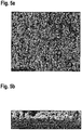
- Ni/Cr foam substrate was covered first with a Si layer of a thickness of about 1500 nm. On the Si layer, an Al layer of a thickness of about 1500 nm was deposited. The Si/Al coated substrate was then heated in the vacuum oven at 180 °C for 60 h. Finally, after etching for 15 min until H 2 gas evolution stopped, flushing and drying, an Aluminum oxide covered porous nanocrystalline Si layer including macropores having a pore width and a pore height of up to several hundred nm, e.g. a pore width of up to 500 nm and a pore height of up to 250 nm, was obtained as shown in the surface SEM and cross-sectional FIB images of Figs. 3a and 3b .
- An above mentioned Ti foil substrate was covered first with a Si layer of a thickness of about 1500 nm.
- an Al layer of a thickness of about 1500 nm was coated.
- the Si/Al coated substrate was then heated in the vacuum oven at 450 °C for 0.5 h. Hence, the temperature was below the eutectic temperature of the Si/Al combination, the eutectic temperature being 577 °C.
- the Al layer on top of the Si layer had a typical polycrystalline microstructure with GBs and grain sizes of 300 to 800 nm (measured by EBSD) in the direction parallel to the surface.
- Fig. 6a shows an XRD pattern of the a-Si (amorphous Si) layer on the Ti substrate.
- Fig. 6a only Ti reflexes are present.
- the XRD pattern is background subtracted.
- the XRD diffraction peaks of Ti substrate, Al template, and Si active material are labelled, indicating for example 2 a highly textured Al/Si system with a (111) grain orientation prior to etching.
- Fig. 6b the XRD pattern of the Al/Si bilayer on the Ti substrate after anneal at 450°C for 30 min is shown, illustrating the crystalline nature of Si and Al.
- a porous nanocrystalline Si layer including macropores having a pore width and a pore height of up to several hundred nm, e.g.
- the porosity was about 60%, determined by physically counting in the surface SEM image the number of pores per unit surface area and evaluating the results using the "straight line" method.
- Fig. 6c shows an XRD pattern of the Si layer of example 2 after annealing and Al etching on the Ti substrate. Fig. 6c illustrates that crystalline Al has disappeared after etching.
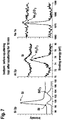
- X-ray photoelectron spectroscopy (XPS) of Si 2p, Al 2p and Na 1s was used to investigate the surface compositions after annealing and Al etching, which were further compared to those at the subsurface (20 nm deep from the surface) by X 1 keV Ar+ sputtering for 10 min.
- XPS X-ray photoelectron spectroscopy
- An above mentioned Ti foil substrate was covered first with a Si layer of a thickness of about 1500 nm. On the Si layer, an Al layer of a thickness of about 150 nm was coated. The Si/Al coated substrate was then heated in the vacuum oven at 600 °C for 0.5 h. Hence, the temperature was above the eutectic temperature of the Si/Al combination, the eutectic temperature being 577 °C.
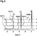
- Fig. 8a is an XRD pattern of the a-Si (amorphous Si) coated Ti substrate of example 3.
- Fig. 8b shows an XRD pattern of the Al coated a-Si layer on the Ti substrate.
- the XRD pattern of the Si layer of example 3 after annealing for 30 min is shown in Fig. 8c.
- Fig. 8d shows the XRD pattern of the Si layer after etching the surface for 30 min. It is clear from Fig. 8d , that polycrystalline Si but essentially no Aluminum oxide is present at the surface, the weak diffraction peak of Si indicating that the nanoporous Si framework is at least partially nanocrystalline.
- Figs. 9 and 10 the results of electrochemical measurements using two-electrode Swagelok-type cells containing the layered samples of example 2 and comparative example 1 are shown.
- the unit C is to be understood in the sense that 1C denotes the current density to theoretically achieve multi-electron reaction to form the L 22 Si 5 phase within 1 h, i.e. it denotes the charge rate to achieve a complete charging of the cell.
- Fig. 9 illustrates the charge capacity of example 2 as a function of cycle number at 0.5 C compared to the charge capacity of comparative example 1, as a life test.
- One cycle is represented by one circle in Fig. 9 .
- the capacity of example 2 was at 1650 mAh/g, i.e. at 55 % of the initial capacity of 3000 mAh/g.
- the capacity is then increased and stabilized at 2000 mAh/g and 1650 mAh/g in the following 150 and 500 cycles, respectively.
- the capacity of comparative example 1 was considerably reduced at 500 cycles.
- the capacity retention of comparative example 1 fades quickly after 100 cycles and drops to 1260 mAh/g and 280 mAh/g at the 160th and 500th cycle respectively. This clearly shows, that example 2 of the invention provides an improved capacity retention as compared to comparative example 1.
- Fig. 10 the charge capacity as a function of cycle number at 0.1 to 8 C in a continuous test of example 2 is shown.
- Each cycle encompassed a complete charging from 0.01 V to 1.5 V and a discharging from 1.5 V to 0.01 V and is represented by one circle in Fig. 10 .
- the cycle period at charge rate 0.1 C was 20 h. 10 cycles were performed at each charge rate.
- the capacity of example 2 is still preserved at about 1800 mAh/g and 1000 mAh/g when the charge rates are as high as 2C and 8C respectively.
- a capacity below 1000 mAh/g at 2C was observed (not shown in Fig. 10 ).
- the Si anode according to example 2 results in a much better rate performance than the coated a-Si anode of comparative example 1.
- embodiments of the invention allow both highly satisfactory capacity retention (e.g. 1650 mAh/g after 500 cycles) and rate performance (e.g. ⁇ 1000 mAh/g at 8C), i.e. a superior durability and life period, for electrodes which include the porous nanocrystalline semiconductor layer of embodiments.
- no binder or additive is required in the method of embodiments of the invention.
- the method of embodiments of the invention allows, as compared to the production of Nanowires, that no pretreatment of the substrate, e.g. in order to promote seed growth of a second phase of the material, is required.
- previous semiconductor nano-material was typically manufactured in complicated chemical deposition processes from explosive and toxic gases using HF. However, in the method according to embodiments of the invention such explosive and toxic agents are not utilized.
- the space between individual nano-sized surface structures i.e. the macropores, can effectively accommodate volume expansion and alleviate strain during lithiation, while being accessible to electrolyte during operation of a lithium-ion battery.
- the method of embodiments is not only beneficial as regards facilitated ion/electron transport pathways and networks in electrodes including the semiconductor layer produced, but also with respect to volume/strain accommodation in the semiconductor layer by semiconductor crystallization and nano-engineering.
- the method of embodiments according to the invention may provide solid electrolytic interphase (SEI) stabilization and/or coulomb efficiency improvement by nano-structuring the semiconductor layer and by an optional coating of an oxidic layer of the metal, which may be conformal and/or ion-conductive.
- SEI solid electrolytic interphase
- an oxidic layer of the metal in which an oxidic layer of the metal is provided on the semiconductor layer, allow avoiding formation of a solid electrolytic interphase, which may deteriorate the battery capacity during operation of the battery.
- the oxidic layer of the metal of embodiments helps to avoid breakage and cracking of the semiconductor layer, to prevent delamination or fracture during lithiation-driven volume expansion.
- ALD Atomic Layer Deposition
- the latter allows forming an oxidic layer of the metal simply during the etching step, e.g. using alkaline solution.
- the method of embodiments of the invention provides a unique nano-engineering of e.g. nanocrystalline Si films, having a thickness of for instance > 0.8 ⁇ m, as Li-ion battery anodes from amorphous Si (a-Si) films based on aluminum-induced crystallization (AIC) and layer exchange processes in Si/Al bilayers.
- a-Si amorphous Si
- AIC aluminum-induced crystallization
- the method of embodiments allows a growth temperature lower than the eutectic one (for Si/Al: 577 °C) without remarkable solubility and diffusivity in the bulk of the metal.
- eutectic one for Si/Al: 577 °C
- nanocrystalline Si films e.g. as thick as 1.5 pm, with a morphology consisting in a high density of isolated nano-structures having columnar shapes can be produced.
- the method of embodiments allows not only a low-temperature crystallization of originally amorphous Si, but may also provide an optional coating of Aluminum oxide which can be generated on almost each Si nano-sized surface structure by facile oxidization of residual Al on Si surfaces during an alkali wash.
- the nano-engineered Si layers of embodiments of the invention are beneficial to the Li-storage kinetics, for instance by a reversible capacity as large as about 1650 mAh/g with a about 99% coulomb efficiency still after an extremely long cycling of 500 times.
Landscapes
- Chemical & Material Sciences (AREA)
- Engineering & Computer Science (AREA)
- Chemical Kinetics & Catalysis (AREA)
- Electrochemistry (AREA)
- General Chemical & Material Sciences (AREA)
- Manufacturing & Machinery (AREA)
- Materials Engineering (AREA)
- Battery Electrode And Active Subsutance (AREA)
Claims (14)
- Procédé de production d'une couche semi-conductrice nanocristalline poreuse, comprenanta) fournir un substrat (10) ayant une surface de substrat (11);b) appliquer une couche semi-conductrice (12) sur la surface du substrat;c) appliquer une couche contenant un métal (14) sur la couche semi-conductrice;d) traiter thermiquement la couche semi-conductrice et la couche contenant du métal à une température (T) et pendant une période de temps (t) telles que la couche semi-conductrice et la couche contenant du métal partiellement interdiffusent et que le semi-conducteur soit au moins partiellement cristallisé; ete) enlever au moins partiellement le métal.
- Procédé de la revendication 1,
dans lequel, à l'étape b), une couche semi-conductrice amorphe (12) est formée; et/ou
dans lequel, à l'étape d), la température et la période de temps sont choisies de telle sorte qu'un semi-conducteur cristallisé (18) soit formé sur une couche interdiffusée (20) comprenant un semi-conducteur cristallisé et le métal; et/ou
dans lequel, à l'étape e), le métal est au moins partiellement éliminé par attaque du substrat revêtu traité thermiquement; et/ou
dans lequel, à l'étape e), une couche oxydique (202) du métal est formée sur la couche semi-conductrice nanocristalline poreuse (200); et/ou
dans lequel, après l'étape e) à une étape f), le matériau semi-conducteur supérieur et/ou lâche est éliminé. - Procédé selon l'une quelconque des revendications précédentes,
dans lequel le semi-conducteur comprend un ou plusieurs semi-conducteurs du groupe IV A du tableau périodique; et/ou
dans lequel le semi-conducteur comprend Si et/ou Ge; et/ou
dans lequel le métal et le semi-conducteur sont partiellement miscibles ou non miscibles; et/ou
dans lequel le métal comprend au moins un métal soluble dans une solution acide et/ou dans une solution alcaline; et/ou
dans lequel le métal comprend au moins un métal choisi parmi Al, Sn, Zn, Ga, In, Pb et Tl; et/ou
dans lequel la couche contenant un métal comprend au moins un élément choisi parmi Al, Sn, Zn, Ga, In, Pb, Tl et Ge; et/ou
dans lequel la couche oxydique du métal est conductrice d'ions; et/ou
dans lequel la couche oxydique du métal est formée conformément à la couche semi-conductrice nanocristalline poreuse. - Procédé selon l'une quelconque des revendications précédentes,
dans lequel le substrat et/ou la surface du substrat est électriquement conducteur; et/ou
dans lequel le substrat et/ou la surface du substrat est choisi parmi Ti, Ni, Cu, Cr, l'acier inoxydable, un polymère électriquement conducteur, une céramique électriquement conductrice ou un mélange de ceux-ci. - Procédé selon l'une quelconque des revendications précédentes,
dans lequel au moins l'une des étapes de revêtement b) et c) comprend un dépôt physique en phase vapeur, un dépôt chimique en phase vapeur; et/ou
dans lequel les étapes a) à f) ou au moins les étapes a) à c) sont réalisées par un procès continu transportant le substrat à travers des chambres de traitement subséquentes; et/ou dans lequel, à l'étape b), une couche semi-conductrice ayant une épaisseur supérieure à 300 nm, de préférence de 300 nm à 5 µm est formée. - Procédé selon l'une quelconque des revendications précédentes,
dans lequel, après l'étape c) et avant l'étape d), une ou plusieurs bicouches de la couche semi-conductrice et de la couche contenant du métal sont appliquées sur la couche contenant du métal; et/ou
dans lequel, à l'étape d), le traitement thermique est effectué à une température inférieure à la température eutectique de la combinaison de semi-conducteur et de métal ou à une température supérieure à la température eutectique de la combinaison de semi-conducteur et de métal; et/ou
dans lequel la relation entre la température (T) [°C] et la période (t) [min] suit au moins 1 / T étant proportionnelle à log t; et/ou
dans lequel, à l'étape d), le traitement thermique est effectué à une température de 160 à 650°C et/ou pendant une période de temps de 0,15 à 72 h. - Procédé selon l'une quelconque des revendications précédentes,
dans lequel, à l'étape d), le traitement thermique est effectué dans une atmosphère de gaz protecteur et/ou sous vide; et/ou
dans lequel, à l'étape e), le substrat revêtu traité thermiquement est attaqué par une solution acide et/ou une solution alcaline. - Couche semi-conductrice nanocristalline poreuse pouvant être obtenue ou obtenue par un procédé selon l'une quelconque des revendications précédentes,
dans lequel la couche semi-conductrice (100; 200) est prévue sur un substrat (10) et comprend une surface externe (102) et des macropores (104) s'étendant de la surface externe de la couche semi-conductrice vers le substrat (10), et
dans lequel les macropores ont une profondeur de 600 à 2100 nm. - Couche semi-conductrice selon la revendication 8,
dans lequel les macropores ont une taille de pores supérieure à 50 nm; et/ou
dans lequel les macropores ont une largeur de 50 à 1000 nm; et/ou
dans lequel les macropores de la couche semi-conductrice sont formés par des espaces intermédiaires de structures de surface (106); et/ou
dans lequel les structures de surface sont cristallines, de taille nano, en trois dimensions, de forme irrégulière et/ou ont la forme d'une colonne; et/ou
dans lequel les structures de surface ont une largeur de 100 à 1000 nm, une hauteur de 100 à 3000 nm et/ou des espaces intermédiaires de 50 à 2100 nm. - Couche semi-conductrice selon la revendication 8 ou 9,
dans lequel l'épaisseur de la couche semi-conductrice est supérieure à 300 nm, de préférence de 300 nm à 5 µm; et/ou
dans lequel les structures de surface semi-conductrices (106) sont revêtues d'une couche oxydique (202) du métal. - Couche semi-conductrice selon l'une quelconque des revendications 8 à 10,
dans lequel le semi-conducteur comprend un ou plusieurs semi-conducteurs du groupe IV A du tableau périodique; et/ou
dans lequel le semi-conducteur comprend Si et/ou Ge; et/ou
dans lequel le métal et le semi-conducteur sont partiellement miscibles ou non miscibles; et/ou
dans lequel le métal comprend au moins un métal soluble dans une solution acide et/ou dans une solution alcaline; et/ou
dans lequel le métal comprend au moins un métal choisi parmi Al, Sn, Zn, Ga, In, Pb et Tl; et/ou
dans lequel la couche oxydique comprend au moins un élément choisi parmi Al, Sn, Zn, Ga, In, Pb, Tl et Ge; et/ou
dans lequel le substrat et/ou la surface du substrat est électriquement conducteur; et/ou
dans lequel le substrat et/ou la surface du substrat est choisi parmi Ti, Ni, Cu, Cr, un acier inoxydable, un polymère électriquement conducteur, une céramique électriquement conductrice ou un mélange de ceux-ci; et/ou
dans lequel la couche oxydique du métal est conductrice des ions et/ou conforme à la couche semi-conductrice nanocristalline poreuse. - Utilisation d'une couche semi-conductrice nanocristalline poreuse selon l'une des revendications 8 à 11 dans une électrode et/ou dans une anode pour un dispositif de stockage d'énergie ou pour une batterie secondaire lithium-ion.
- Anode pour une batterie secondaire lithium-ion, comprenant la couche semi-conductrice nanocristalline poreuse selon l'une des revendications 8 à 11.
- Batterie secondaire lithium-ion comprenant une anode selon la revendication 13.
Applications Claiming Priority (1)
| Application Number | Priority Date | Filing Date | Title |
|---|---|---|---|
| PCT/EP2013/077916 WO2015096854A1 (fr) | 2013-12-23 | 2013-12-23 | Procédé de fabrication de couche semi-conductrice nanocristalline poreuse, couche semi-conductrice nanocristalline poreuse, utilisation de cette dernière, anode et batterie lithium-ion secondaire |
Publications (2)
| Publication Number | Publication Date |
|---|---|
| EP3087629A1 EP3087629A1 (fr) | 2016-11-02 |
| EP3087629B1 true EP3087629B1 (fr) | 2019-03-27 |
Family
ID=49883113
Family Applications (1)
| Application Number | Title | Priority Date | Filing Date |
|---|---|---|---|
| EP13814164.3A Not-in-force EP3087629B1 (fr) | 2013-12-23 | 2013-12-23 | Procédé de fabrication de couche semi-conductrice nanocristalline poreuse, couche semi-conductrice nanocristalline poreuse, utilisation de cette dernière, anode et batterie lithium-ion secondaire |
Country Status (3)
| Country | Link |
|---|---|
| US (1) | US20160322632A1 (fr) |
| EP (1) | EP3087629B1 (fr) |
| WO (1) | WO2015096854A1 (fr) |
Families Citing this family (11)
| Publication number | Priority date | Publication date | Assignee | Title |
|---|---|---|---|---|
| TWI562703B (en) * | 2015-10-06 | 2016-12-11 | Rigidtecn Microelectronics Corp | Protective cover and appearance |
| US9780103B2 (en) | 2015-11-16 | 2017-10-03 | Micron Technology, Inc. | Methods of forming integrated structures |
| CN107799387A (zh) * | 2016-09-06 | 2018-03-13 | 中国科学院上海微系统与信息技术研究所 | 一种在掺杂的多晶硅层上制备硅纳米线的方法及结构 |
| CN107089664B (zh) * | 2017-04-13 | 2020-01-07 | 济南大学 | 一种纳米多孔硅材料的制备方法 |
| US20180366768A1 (en) * | 2017-06-19 | 2018-12-20 | Neah Power Systems, Inc. | Porous Silicon One-Wafer Battery with Voltage Enhancement by Internal Field |
| WO2019227016A1 (fr) * | 2018-05-24 | 2019-11-28 | 24M Technologies, Inc. | Électrodes à gradient, à haute densité d'énergie, et procédés pour leur fabrication |
| US11189724B2 (en) * | 2018-10-24 | 2021-11-30 | International Business Machines Corporation | Method of forming a top epitaxy source/drain structure for a vertical transistor |
| US11984580B2 (en) * | 2019-05-06 | 2024-05-14 | Honeycomb Battery Company | Protected anode active material particles for rechargeable lithium batteries |
| CN113416950B (zh) * | 2021-06-08 | 2022-07-22 | 吉林化工学院 | 一种基于稀土纳米颗粒的铜合金表面预处理装置和方法 |
| US12444729B2 (en) * | 2022-01-14 | 2025-10-14 | The Chinese University Of Hong Kong | Preparation of LI and NA foils with {110} or {100} surface texturing |
| CN121091569B (zh) * | 2025-08-25 | 2026-05-12 | 中国科学院上海硅酸盐研究所 | 一种透过型宽色域全固态电致变色显示器及其制备方法 |
Family Cites Families (2)
| Publication number | Priority date | Publication date | Assignee | Title |
|---|---|---|---|---|
| US7361313B2 (en) * | 2003-02-18 | 2008-04-22 | Intel Corporation | Methods for uniform metal impregnation into a nanoporous material |
| US9139441B2 (en) * | 2012-01-19 | 2015-09-22 | Envia Systems, Inc. | Porous silicon based anode material formed using metal reduction |
-
2013
- 2013-12-23 US US15/107,583 patent/US20160322632A1/en not_active Abandoned
- 2013-12-23 EP EP13814164.3A patent/EP3087629B1/fr not_active Not-in-force
- 2013-12-23 WO PCT/EP2013/077916 patent/WO2015096854A1/fr not_active Ceased
Non-Patent Citations (1)
| Title |
|---|
| None * |
Also Published As
| Publication number | Publication date |
|---|---|
| WO2015096854A1 (fr) | 2015-07-02 |
| US20160322632A1 (en) | 2016-11-03 |
| EP3087629A1 (fr) | 2016-11-02 |
Similar Documents
| Publication | Publication Date | Title |
|---|---|---|
| US20160322632A1 (en) | Method for producing a porous nanocrystalline semiconductor layer, porous nanocrystalline semiconductor layer, use thereof, anode, and secondary lithium-ion battery | |
| KR102946868B1 (ko) | 배터리 애노드로서 사용하기 위한 실리콘 조성 물질 | |
| JP7365658B2 (ja) | リチウム系エネルギー貯蔵デバイスのアノード | |
| CA2987938C (fr) | Revetements nano-modifies pour materiaux actifs d'anode, materiaux actifs de cathode, et electrolytes solides et procedes de fabrication de batteries contenant des revetements nan o-modifies | |
| KR102139736B1 (ko) | 복합음극활물질, 이의 제조 방법 및 이를 포함하는 음극을 구비한 리튬이차전지 | |
| EP2489088B1 (fr) | Batterie lithium-soufre nanostructurée et son procédé de fabrication | |
| US8142569B2 (en) | Apparatus for forming structured material for energy storage device and method | |
| US20230094444A1 (en) | Method of producing electrode material for lithium-ion secondary battery and lithium-ion battery using such electrode material | |
| US10403889B2 (en) | High-capacity silicon nanowire based anode for lithium-ion batteries | |
| KR101665099B1 (ko) | 천연흑연과 금속물질을 포함하는 리튬이온 이차전지용 음극 활물질 및 이의 제조방법 | |
| US9548493B2 (en) | Porous composite and manufacturing method thereof | |
| KR102417034B1 (ko) | 하이브리드 나노구조 물질 및 이의 제조 방법 | |
| Hao et al. | Ionic liquid electrodeposition of strain-released Germanium nanowires as stable anodes for lithium ion batteries | |
| KR102921772B1 (ko) | 복합 입자, 부극재 및 리튬 이온 이차 전지 | |
| GB2502625A (en) | Method of forming Silicon | |
| WO2011053736A1 (fr) | Anodes d'accumulateur en silicium structuré | |
| Qu et al. | Metal-induced crystallization of highly corrugated silicon thick films as potential anodes for Li-ion batteries | |
| KR20150135493A (ko) | 개질된 다결정 리튬 금속 포스페이트를 포함하는 세라믹 전해질 물질 | |
| Loveridge et al. | Binder-free Sn–Si heterostructure films for high capacity Li-ion batteries | |
| CN111936419B (zh) | 硅锂离子电极材料 | |
| CN117480119A (zh) | 作为储能装置中的电极材料的石墨烯纳米带 | |
| KR102423246B1 (ko) | 그래핀층을 포함하는 집전체, 이를 포함하는 리튬이온전지 및 슈퍼커패시터 | |
| Kim et al. | Bundle-type silicon nanorod anodes produced by electroless etching using silver ions and their electrochemical characteristics in lithium ion cells | |
| HK40068604A (en) | Silicon composition material for use as battery anode | |
| Kennedy | Nano-structuring of silicon and germanium: a viable route to high capacity, long cycle life lithium-ion battery electrodes |
Legal Events
| Date | Code | Title | Description |
|---|---|---|---|
| PUAI | Public reference made under article 153(3) epc to a published international application that has entered the european phase |
Free format text: ORIGINAL CODE: 0009012 |
|
| 17P | Request for examination filed |
Effective date: 20160708 |
|
| AK | Designated contracting states |
Kind code of ref document: A1 Designated state(s): AL AT BE BG CH CY CZ DE DK EE ES FI FR GB GR HR HU IE IS IT LI LT LU LV MC MK MT NL NO PL PT RO RS SE SI SK SM TR |
|
| AX | Request for extension of the european patent |
Extension state: BA ME |
|
| DAX | Request for extension of the european patent (deleted) | ||
| STAA | Information on the status of an ep patent application or granted ep patent |
Free format text: STATUS: EXAMINATION IS IN PROGRESS |
|
| 17Q | First examination report despatched |
Effective date: 20180326 |
|
| RIC1 | Information provided on ipc code assigned before grant |
Ipc: H01M 4/02 20060101ALN20180816BHEP Ipc: H01L 21/02 20060101ALN20180816BHEP Ipc: H01M 4/04 20060101AFI20180816BHEP Ipc: H01M 10/052 20100101ALN20180816BHEP Ipc: H01M 4/134 20100101ALI20180816BHEP Ipc: H01M 4/1395 20100101ALI20180816BHEP Ipc: H01M 4/38 20060101ALI20180816BHEP |
|
| GRAP | Despatch of communication of intention to grant a patent |
Free format text: ORIGINAL CODE: EPIDOSNIGR1 |
|
| STAA | Information on the status of an ep patent application or granted ep patent |
Free format text: STATUS: GRANT OF PATENT IS INTENDED |
|
| INTG | Intention to grant announced |
Effective date: 20180921 |
|
| GRAS | Grant fee paid |
Free format text: ORIGINAL CODE: EPIDOSNIGR3 |
|
| GRAJ | Information related to disapproval of communication of intention to grant by the applicant or resumption of examination proceedings by the epo deleted |
Free format text: ORIGINAL CODE: EPIDOSDIGR1 |
|
| GRAL | Information related to payment of fee for publishing/printing deleted |
Free format text: ORIGINAL CODE: EPIDOSDIGR3 |
|
| STAA | Information on the status of an ep patent application or granted ep patent |
Free format text: STATUS: EXAMINATION IS IN PROGRESS |
|
| GRAR | Information related to intention to grant a patent recorded |
Free format text: ORIGINAL CODE: EPIDOSNIGR71 |
|
| STAA | Information on the status of an ep patent application or granted ep patent |
Free format text: STATUS: GRANT OF PATENT IS INTENDED |
|
| GRAA | (expected) grant |
Free format text: ORIGINAL CODE: 0009210 |
|
| STAA | Information on the status of an ep patent application or granted ep patent |
Free format text: STATUS: THE PATENT HAS BEEN GRANTED |
|
| INTC | Intention to grant announced (deleted) | ||
| RIC1 | Information provided on ipc code assigned before grant |
Ipc: H01L 21/02 20060101ALN20190131BHEP Ipc: H01M 4/38 20060101ALI20190131BHEP Ipc: H01M 4/134 20100101ALI20190131BHEP Ipc: H01M 4/04 20060101AFI20190131BHEP Ipc: H01M 4/02 20060101ALN20190131BHEP Ipc: H01M 10/052 20100101ALN20190131BHEP Ipc: H01M 4/1395 20100101ALI20190131BHEP |
|
| INTG | Intention to grant announced |
Effective date: 20190212 |
|
| AK | Designated contracting states |
Kind code of ref document: B1 Designated state(s): AL AT BE BG CH CY CZ DE DK EE ES FI FR GB GR HR HU IE IS IT LI LT LU LV MC MK MT NL NO PL PT RO RS SE SI SK SM TR |
|
| REG | Reference to a national code |
Ref country code: GB Ref legal event code: FG4D |
|
| REG | Reference to a national code |
Ref country code: CH Ref legal event code: EP |
|
| REG | Reference to a national code |
Ref country code: AT Ref legal event code: REF Ref document number: 1114112 Country of ref document: AT Kind code of ref document: T Effective date: 20190415 |
|
| REG | Reference to a national code |
Ref country code: IE Ref legal event code: FG4D |
|
| REG | Reference to a national code |
Ref country code: DE Ref legal event code: R096 Ref document number: 602013053042 Country of ref document: DE |
|
| PG25 | Lapsed in a contracting state [announced via postgrant information from national office to epo] |
Ref country code: SE Free format text: LAPSE BECAUSE OF FAILURE TO SUBMIT A TRANSLATION OF THE DESCRIPTION OR TO PAY THE FEE WITHIN THE PRESCRIBED TIME-LIMIT Effective date: 20190327 Ref country code: NO Free format text: LAPSE BECAUSE OF FAILURE TO SUBMIT A TRANSLATION OF THE DESCRIPTION OR TO PAY THE FEE WITHIN THE PRESCRIBED TIME-LIMIT Effective date: 20190627 Ref country code: FI Free format text: LAPSE BECAUSE OF FAILURE TO SUBMIT A TRANSLATION OF THE DESCRIPTION OR TO PAY THE FEE WITHIN THE PRESCRIBED TIME-LIMIT Effective date: 20190327 Ref country code: LT Free format text: LAPSE BECAUSE OF FAILURE TO SUBMIT A TRANSLATION OF THE DESCRIPTION OR TO PAY THE FEE WITHIN THE PRESCRIBED TIME-LIMIT Effective date: 20190327 |
|
| REG | Reference to a national code |
Ref country code: NL Ref legal event code: MP Effective date: 20190327 |
|
| PG25 | Lapsed in a contracting state [announced via postgrant information from national office to epo] |
Ref country code: NL Free format text: LAPSE BECAUSE OF FAILURE TO SUBMIT A TRANSLATION OF THE DESCRIPTION OR TO PAY THE FEE WITHIN THE PRESCRIBED TIME-LIMIT Effective date: 20190327 Ref country code: HR Free format text: LAPSE BECAUSE OF FAILURE TO SUBMIT A TRANSLATION OF THE DESCRIPTION OR TO PAY THE FEE WITHIN THE PRESCRIBED TIME-LIMIT Effective date: 20190327 Ref country code: LV Free format text: LAPSE BECAUSE OF FAILURE TO SUBMIT A TRANSLATION OF THE DESCRIPTION OR TO PAY THE FEE WITHIN THE PRESCRIBED TIME-LIMIT Effective date: 20190327 Ref country code: GR Free format text: LAPSE BECAUSE OF FAILURE TO SUBMIT A TRANSLATION OF THE DESCRIPTION OR TO PAY THE FEE WITHIN THE PRESCRIBED TIME-LIMIT Effective date: 20190628 Ref country code: BG Free format text: LAPSE BECAUSE OF FAILURE TO SUBMIT A TRANSLATION OF THE DESCRIPTION OR TO PAY THE FEE WITHIN THE PRESCRIBED TIME-LIMIT Effective date: 20190627 Ref country code: RS Free format text: LAPSE BECAUSE OF FAILURE TO SUBMIT A TRANSLATION OF THE DESCRIPTION OR TO PAY THE FEE WITHIN THE PRESCRIBED TIME-LIMIT Effective date: 20190327 |
|
| REG | Reference to a national code |
Ref country code: AT Ref legal event code: MK05 Ref document number: 1114112 Country of ref document: AT Kind code of ref document: T Effective date: 20190327 |
|
| PG25 | Lapsed in a contracting state [announced via postgrant information from national office to epo] |
Ref country code: AL Free format text: LAPSE BECAUSE OF FAILURE TO SUBMIT A TRANSLATION OF THE DESCRIPTION OR TO PAY THE FEE WITHIN THE PRESCRIBED TIME-LIMIT Effective date: 20190327 Ref country code: PT Free format text: LAPSE BECAUSE OF FAILURE TO SUBMIT A TRANSLATION OF THE DESCRIPTION OR TO PAY THE FEE WITHIN THE PRESCRIBED TIME-LIMIT Effective date: 20190727 Ref country code: ES Free format text: LAPSE BECAUSE OF FAILURE TO SUBMIT A TRANSLATION OF THE DESCRIPTION OR TO PAY THE FEE WITHIN THE PRESCRIBED TIME-LIMIT Effective date: 20190327 Ref country code: CZ Free format text: LAPSE BECAUSE OF FAILURE TO SUBMIT A TRANSLATION OF THE DESCRIPTION OR TO PAY THE FEE WITHIN THE PRESCRIBED TIME-LIMIT Effective date: 20190327 Ref country code: RO Free format text: LAPSE BECAUSE OF FAILURE TO SUBMIT A TRANSLATION OF THE DESCRIPTION OR TO PAY THE FEE WITHIN THE PRESCRIBED TIME-LIMIT Effective date: 20190327 Ref country code: IT Free format text: LAPSE BECAUSE OF FAILURE TO SUBMIT A TRANSLATION OF THE DESCRIPTION OR TO PAY THE FEE WITHIN THE PRESCRIBED TIME-LIMIT Effective date: 20190327 Ref country code: EE Free format text: LAPSE BECAUSE OF FAILURE TO SUBMIT A TRANSLATION OF THE DESCRIPTION OR TO PAY THE FEE WITHIN THE PRESCRIBED TIME-LIMIT Effective date: 20190327 Ref country code: SK Free format text: LAPSE BECAUSE OF FAILURE TO SUBMIT A TRANSLATION OF THE DESCRIPTION OR TO PAY THE FEE WITHIN THE PRESCRIBED TIME-LIMIT Effective date: 20190327 |
|
| PG25 | Lapsed in a contracting state [announced via postgrant information from national office to epo] |
Ref country code: PL Free format text: LAPSE BECAUSE OF FAILURE TO SUBMIT A TRANSLATION OF THE DESCRIPTION OR TO PAY THE FEE WITHIN THE PRESCRIBED TIME-LIMIT Effective date: 20190327 Ref country code: SM Free format text: LAPSE BECAUSE OF FAILURE TO SUBMIT A TRANSLATION OF THE DESCRIPTION OR TO PAY THE FEE WITHIN THE PRESCRIBED TIME-LIMIT Effective date: 20190327 |
|
| PG25 | Lapsed in a contracting state [announced via postgrant information from national office to epo] |
Ref country code: IS Free format text: LAPSE BECAUSE OF FAILURE TO SUBMIT A TRANSLATION OF THE DESCRIPTION OR TO PAY THE FEE WITHIN THE PRESCRIBED TIME-LIMIT Effective date: 20190727 Ref country code: AT Free format text: LAPSE BECAUSE OF FAILURE TO SUBMIT A TRANSLATION OF THE DESCRIPTION OR TO PAY THE FEE WITHIN THE PRESCRIBED TIME-LIMIT Effective date: 20190327 |
|
| REG | Reference to a national code |
Ref country code: DE Ref legal event code: R097 Ref document number: 602013053042 Country of ref document: DE |
|
| PG25 | Lapsed in a contracting state [announced via postgrant information from national office to epo] |
Ref country code: DK Free format text: LAPSE BECAUSE OF FAILURE TO SUBMIT A TRANSLATION OF THE DESCRIPTION OR TO PAY THE FEE WITHIN THE PRESCRIBED TIME-LIMIT Effective date: 20190327 |
|
| PLBE | No opposition filed within time limit |
Free format text: ORIGINAL CODE: 0009261 |
|
| STAA | Information on the status of an ep patent application or granted ep patent |
Free format text: STATUS: NO OPPOSITION FILED WITHIN TIME LIMIT |
|
| PG25 | Lapsed in a contracting state [announced via postgrant information from national office to epo] |
Ref country code: SI Free format text: LAPSE BECAUSE OF FAILURE TO SUBMIT A TRANSLATION OF THE DESCRIPTION OR TO PAY THE FEE WITHIN THE PRESCRIBED TIME-LIMIT Effective date: 20190327 |
|
| 26N | No opposition filed |
Effective date: 20200103 |
|
| PG25 | Lapsed in a contracting state [announced via postgrant information from national office to epo] |
Ref country code: TR Free format text: LAPSE BECAUSE OF FAILURE TO SUBMIT A TRANSLATION OF THE DESCRIPTION OR TO PAY THE FEE WITHIN THE PRESCRIBED TIME-LIMIT Effective date: 20190327 |
|
| REG | Reference to a national code |
Ref country code: CH Ref legal event code: PL |
|
| REG | Reference to a national code |
Ref country code: BE Ref legal event code: MM Effective date: 20191231 |
|
| PG25 | Lapsed in a contracting state [announced via postgrant information from national office to epo] |
Ref country code: MC Free format text: LAPSE BECAUSE OF FAILURE TO SUBMIT A TRANSLATION OF THE DESCRIPTION OR TO PAY THE FEE WITHIN THE PRESCRIBED TIME-LIMIT Effective date: 20190327 |
|
| PG25 | Lapsed in a contracting state [announced via postgrant information from national office to epo] |
Ref country code: IE Free format text: LAPSE BECAUSE OF NON-PAYMENT OF DUE FEES Effective date: 20191223 Ref country code: LU Free format text: LAPSE BECAUSE OF NON-PAYMENT OF DUE FEES Effective date: 20191223 |
|
| PG25 | Lapsed in a contracting state [announced via postgrant information from national office to epo] |
Ref country code: CH Free format text: LAPSE BECAUSE OF NON-PAYMENT OF DUE FEES Effective date: 20191231 Ref country code: BE Free format text: LAPSE BECAUSE OF NON-PAYMENT OF DUE FEES Effective date: 20191231 Ref country code: LI Free format text: LAPSE BECAUSE OF NON-PAYMENT OF DUE FEES Effective date: 20191231 |
|
| PG25 | Lapsed in a contracting state [announced via postgrant information from national office to epo] |
Ref country code: CY Free format text: LAPSE BECAUSE OF FAILURE TO SUBMIT A TRANSLATION OF THE DESCRIPTION OR TO PAY THE FEE WITHIN THE PRESCRIBED TIME-LIMIT Effective date: 20190327 |
|
| PG25 | Lapsed in a contracting state [announced via postgrant information from national office to epo] |
Ref country code: HU Free format text: LAPSE BECAUSE OF FAILURE TO SUBMIT A TRANSLATION OF THE DESCRIPTION OR TO PAY THE FEE WITHIN THE PRESCRIBED TIME-LIMIT; INVALID AB INITIO Effective date: 20131223 Ref country code: MT Free format text: LAPSE BECAUSE OF FAILURE TO SUBMIT A TRANSLATION OF THE DESCRIPTION OR TO PAY THE FEE WITHIN THE PRESCRIBED TIME-LIMIT Effective date: 20190327 |
|
| PGFP | Annual fee paid to national office [announced via postgrant information from national office to epo] |
Ref country code: FR Payment date: 20210617 Year of fee payment: 8 |
|
| PGFP | Annual fee paid to national office [announced via postgrant information from national office to epo] |
Ref country code: GB Payment date: 20210625 Year of fee payment: 8 |
|
| PGFP | Annual fee paid to national office [announced via postgrant information from national office to epo] |
Ref country code: DE Payment date: 20211223 Year of fee payment: 9 |
|
| PG25 | Lapsed in a contracting state [announced via postgrant information from national office to epo] |
Ref country code: MK Free format text: LAPSE BECAUSE OF FAILURE TO SUBMIT A TRANSLATION OF THE DESCRIPTION OR TO PAY THE FEE WITHIN THE PRESCRIBED TIME-LIMIT Effective date: 20190327 |
|
| GBPC | Gb: european patent ceased through non-payment of renewal fee |
Effective date: 20211223 |
|
| PG25 | Lapsed in a contracting state [announced via postgrant information from national office to epo] |
Ref country code: GB Free format text: LAPSE BECAUSE OF NON-PAYMENT OF DUE FEES Effective date: 20211223 |
|
| PG25 | Lapsed in a contracting state [announced via postgrant information from national office to epo] |
Ref country code: FR Free format text: LAPSE BECAUSE OF NON-PAYMENT OF DUE FEES Effective date: 20211231 |
|
| REG | Reference to a national code |
Ref country code: DE Ref legal event code: R119 Ref document number: 602013053042 Country of ref document: DE |
|
| PG25 | Lapsed in a contracting state [announced via postgrant information from national office to epo] |
Ref country code: DE Free format text: LAPSE BECAUSE OF NON-PAYMENT OF DUE FEES Effective date: 20230701 |