EP3088950B1 - Lichtemittierendes diodenpaket, rückbeleuchtungseinheit, und anzeigevorrichtung mit einer lichtumwandlungsplatte - Google Patents
Lichtemittierendes diodenpaket, rückbeleuchtungseinheit, und anzeigevorrichtung mit einer lichtumwandlungsplatte Download PDFInfo
- Publication number
- EP3088950B1 EP3088950B1 EP15002904.9A EP15002904A EP3088950B1 EP 3088950 B1 EP3088950 B1 EP 3088950B1 EP 15002904 A EP15002904 A EP 15002904A EP 3088950 B1 EP3088950 B1 EP 3088950B1
- Authority
- EP
- European Patent Office
- Prior art keywords
- light
- emitting diode
- disposed
- glass substrate
- light conversion
- Prior art date
- Legal status (The legal status is an assumption and is not a legal conclusion. Google has not performed a legal analysis and makes no representation as to the accuracy of the status listed.)
- Active
Links
Images


Classifications
-
- H—ELECTRICITY
- H10—SEMICONDUCTOR DEVICES; ELECTRIC SOLID-STATE DEVICES NOT OTHERWISE PROVIDED FOR
- H10H—INORGANIC LIGHT-EMITTING SEMICONDUCTOR DEVICES HAVING POTENTIAL BARRIERS
- H10H20/00—Individual inorganic light-emitting semiconductor devices having potential barriers, e.g. light-emitting diodes [LED]
- H10H20/80—Constructional details
- H10H20/85—Packages
- H10H20/851—Wavelength conversion means
- H10H20/8514—Wavelength conversion means characterised by their shape, e.g. plate or foil
-
- G—PHYSICS
- G02—OPTICS
- G02F—OPTICAL DEVICES OR ARRANGEMENTS FOR THE CONTROL OF LIGHT BY MODIFICATION OF THE OPTICAL PROPERTIES OF THE MEDIA OF THE ELEMENTS INVOLVED THEREIN; NON-LINEAR OPTICS; FREQUENCY-CHANGING OF LIGHT; OPTICAL LOGIC ELEMENTS; OPTICAL ANALOGUE/DIGITAL CONVERTERS
- G02F1/00—Devices or arrangements for the control of the intensity, colour, phase, polarisation or direction of light arriving from an independent light source, e.g. switching, gating or modulating; Non-linear optics
- G02F1/01—Devices or arrangements for the control of the intensity, colour, phase, polarisation or direction of light arriving from an independent light source, e.g. switching, gating or modulating; Non-linear optics for the control of the intensity, phase, polarisation or colour
- G02F1/13—Devices or arrangements for the control of the intensity, colour, phase, polarisation or direction of light arriving from an independent light source, e.g. switching, gating or modulating; Non-linear optics for the control of the intensity, phase, polarisation or colour based on liquid crystals, e.g. single liquid crystal display cells
- G02F1/133—Constructional arrangements; Operation of liquid crystal cells; Circuit arrangements
- G02F1/1333—Constructional arrangements; Manufacturing methods
- G02F1/1335—Structural association of cells with optical devices, e.g. polarisers or reflectors
- G02F1/1336—Illuminating devices
-
- F—MECHANICAL ENGINEERING; LIGHTING; HEATING; WEAPONS; BLASTING
- F21—LIGHTING
- F21V—FUNCTIONAL FEATURES OR DETAILS OF LIGHTING DEVICES OR SYSTEMS THEREOF; STRUCTURAL COMBINATIONS OF LIGHTING DEVICES WITH OTHER ARTICLES, NOT OTHERWISE PROVIDED FOR
- F21V13/00—Producing particular characteristics or distribution of the light emitted by means of a combination of elements specified in two or more of main groups F21V1/00 - F21V11/00
- F21V13/12—Combinations of only three kinds of elements
- F21V13/14—Combinations of only three kinds of elements the elements being filters or photoluminescent elements, reflectors and refractors
-
- F—MECHANICAL ENGINEERING; LIGHTING; HEATING; WEAPONS; BLASTING
- F21—LIGHTING
- F21V—FUNCTIONAL FEATURES OR DETAILS OF LIGHTING DEVICES OR SYSTEMS THEREOF; STRUCTURAL COMBINATIONS OF LIGHTING DEVICES WITH OTHER ARTICLES, NOT OTHERWISE PROVIDED FOR
- F21V9/00—Elements for modifying spectral properties, polarisation or intensity of the light emitted, e.g. filters
- F21V9/30—Elements containing photoluminescent material distinct from or spaced from the light source
- F21V9/32—Elements containing photoluminescent material distinct from or spaced from the light source characterised by the arrangement of the photoluminescent material
-
- G—PHYSICS
- G02—OPTICS
- G02B—OPTICAL ELEMENTS, SYSTEMS OR APPARATUS
- G02B6/00—Light guides; Structural details of arrangements comprising light guides and other optical elements, e.g. couplings
- G02B6/0001—Light guides; Structural details of arrangements comprising light guides and other optical elements, e.g. couplings specially adapted for lighting devices or systems
- G02B6/0011—Light guides; Structural details of arrangements comprising light guides and other optical elements, e.g. couplings specially adapted for lighting devices or systems the light guides being planar or of plate-like form
- G02B6/0013—Means for improving the coupling-in of light from the light source into the light guide
- G02B6/0023—Means for improving the coupling-in of light from the light source into the light guide provided by one optical element, or plurality thereof, placed between the light guide and the light source, or around the light source
- G02B6/0031—Reflecting element, sheet or layer
-
- G—PHYSICS
- G02—OPTICS
- G02B—OPTICAL ELEMENTS, SYSTEMS OR APPARATUS
- G02B6/00—Light guides; Structural details of arrangements comprising light guides and other optical elements, e.g. couplings
- G02B6/0001—Light guides; Structural details of arrangements comprising light guides and other optical elements, e.g. couplings specially adapted for lighting devices or systems
- G02B6/0011—Light guides; Structural details of arrangements comprising light guides and other optical elements, e.g. couplings specially adapted for lighting devices or systems the light guides being planar or of plate-like form
- G02B6/0066—Light guides; Structural details of arrangements comprising light guides and other optical elements, e.g. couplings specially adapted for lighting devices or systems the light guides being planar or of plate-like form characterised by the light source being coupled to the light guide
- G02B6/0073—Light emitting diode [LED]
-
- G—PHYSICS
- G02—OPTICS
- G02F—OPTICAL DEVICES OR ARRANGEMENTS FOR THE CONTROL OF LIGHT BY MODIFICATION OF THE OPTICAL PROPERTIES OF THE MEDIA OF THE ELEMENTS INVOLVED THEREIN; NON-LINEAR OPTICS; FREQUENCY-CHANGING OF LIGHT; OPTICAL LOGIC ELEMENTS; OPTICAL ANALOGUE/DIGITAL CONVERTERS
- G02F1/00—Devices or arrangements for the control of the intensity, colour, phase, polarisation or direction of light arriving from an independent light source, e.g. switching, gating or modulating; Non-linear optics
- G02F1/01—Devices or arrangements for the control of the intensity, colour, phase, polarisation or direction of light arriving from an independent light source, e.g. switching, gating or modulating; Non-linear optics for the control of the intensity, phase, polarisation or colour
- G02F1/13—Devices or arrangements for the control of the intensity, colour, phase, polarisation or direction of light arriving from an independent light source, e.g. switching, gating or modulating; Non-linear optics for the control of the intensity, phase, polarisation or colour based on liquid crystals, e.g. single liquid crystal display cells
- G02F1/133—Constructional arrangements; Operation of liquid crystal cells; Circuit arrangements
- G02F1/1333—Constructional arrangements; Manufacturing methods
- G02F1/1335—Structural association of cells with optical devices, e.g. polarisers or reflectors
- G02F1/1336—Illuminating devices
- G02F1/133602—Direct backlight
- G02F1/133603—Direct backlight with LEDs
-
- G—PHYSICS
- G02—OPTICS
- G02F—OPTICAL DEVICES OR ARRANGEMENTS FOR THE CONTROL OF LIGHT BY MODIFICATION OF THE OPTICAL PROPERTIES OF THE MEDIA OF THE ELEMENTS INVOLVED THEREIN; NON-LINEAR OPTICS; FREQUENCY-CHANGING OF LIGHT; OPTICAL LOGIC ELEMENTS; OPTICAL ANALOGUE/DIGITAL CONVERTERS
- G02F1/00—Devices or arrangements for the control of the intensity, colour, phase, polarisation or direction of light arriving from an independent light source, e.g. switching, gating or modulating; Non-linear optics
- G02F1/01—Devices or arrangements for the control of the intensity, colour, phase, polarisation or direction of light arriving from an independent light source, e.g. switching, gating or modulating; Non-linear optics for the control of the intensity, phase, polarisation or colour
- G02F1/13—Devices or arrangements for the control of the intensity, colour, phase, polarisation or direction of light arriving from an independent light source, e.g. switching, gating or modulating; Non-linear optics for the control of the intensity, phase, polarisation or colour based on liquid crystals, e.g. single liquid crystal display cells
- G02F1/133—Constructional arrangements; Operation of liquid crystal cells; Circuit arrangements
- G02F1/1333—Constructional arrangements; Manufacturing methods
- G02F1/1335—Structural association of cells with optical devices, e.g. polarisers or reflectors
- G02F1/1336—Illuminating devices
- G02F1/133602—Direct backlight
- G02F1/133606—Direct backlight including a specially adapted diffusing, scattering or light controlling members
-
- G—PHYSICS
- G02—OPTICS
- G02F—OPTICAL DEVICES OR ARRANGEMENTS FOR THE CONTROL OF LIGHT BY MODIFICATION OF THE OPTICAL PROPERTIES OF THE MEDIA OF THE ELEMENTS INVOLVED THEREIN; NON-LINEAR OPTICS; FREQUENCY-CHANGING OF LIGHT; OPTICAL LOGIC ELEMENTS; OPTICAL ANALOGUE/DIGITAL CONVERTERS
- G02F1/00—Devices or arrangements for the control of the intensity, colour, phase, polarisation or direction of light arriving from an independent light source, e.g. switching, gating or modulating; Non-linear optics
- G02F1/01—Devices or arrangements for the control of the intensity, colour, phase, polarisation or direction of light arriving from an independent light source, e.g. switching, gating or modulating; Non-linear optics for the control of the intensity, phase, polarisation or colour
- G02F1/13—Devices or arrangements for the control of the intensity, colour, phase, polarisation or direction of light arriving from an independent light source, e.g. switching, gating or modulating; Non-linear optics for the control of the intensity, phase, polarisation or colour based on liquid crystals, e.g. single liquid crystal display cells
- G02F1/133—Constructional arrangements; Operation of liquid crystal cells; Circuit arrangements
- G02F1/1333—Constructional arrangements; Manufacturing methods
- G02F1/1335—Structural association of cells with optical devices, e.g. polarisers or reflectors
- G02F1/1336—Illuminating devices
- G02F1/133615—Edge-illuminating devices, i.e. illuminating from the side
-
- G—PHYSICS
- G02—OPTICS
- G02F—OPTICAL DEVICES OR ARRANGEMENTS FOR THE CONTROL OF LIGHT BY MODIFICATION OF THE OPTICAL PROPERTIES OF THE MEDIA OF THE ELEMENTS INVOLVED THEREIN; NON-LINEAR OPTICS; FREQUENCY-CHANGING OF LIGHT; OPTICAL LOGIC ELEMENTS; OPTICAL ANALOGUE/DIGITAL CONVERTERS
- G02F2/00—Demodulating light; Transferring the modulation of modulated light; Frequency-changing of light
- G02F2/02—Frequency-changing of light, e.g. by quantum counters
-
- H—ELECTRICITY
- H10—SEMICONDUCTOR DEVICES; ELECTRIC SOLID-STATE DEVICES NOT OTHERWISE PROVIDED FOR
- H10H—INORGANIC LIGHT-EMITTING SEMICONDUCTOR DEVICES HAVING POTENTIAL BARRIERS
- H10H20/00—Individual inorganic light-emitting semiconductor devices having potential barriers, e.g. light-emitting diodes [LED]
- H10H20/80—Constructional details
- H10H20/85—Packages
- H10H20/851—Wavelength conversion means
- H10H20/8511—Wavelength conversion means characterised by their material, e.g. binder
-
- G—PHYSICS
- G02—OPTICS
- G02F—OPTICAL DEVICES OR ARRANGEMENTS FOR THE CONTROL OF LIGHT BY MODIFICATION OF THE OPTICAL PROPERTIES OF THE MEDIA OF THE ELEMENTS INVOLVED THEREIN; NON-LINEAR OPTICS; FREQUENCY-CHANGING OF LIGHT; OPTICAL LOGIC ELEMENTS; OPTICAL ANALOGUE/DIGITAL CONVERTERS
- G02F1/00—Devices or arrangements for the control of the intensity, colour, phase, polarisation or direction of light arriving from an independent light source, e.g. switching, gating or modulating; Non-linear optics
- G02F1/01—Devices or arrangements for the control of the intensity, colour, phase, polarisation or direction of light arriving from an independent light source, e.g. switching, gating or modulating; Non-linear optics for the control of the intensity, phase, polarisation or colour
- G02F1/13—Devices or arrangements for the control of the intensity, colour, phase, polarisation or direction of light arriving from an independent light source, e.g. switching, gating or modulating; Non-linear optics for the control of the intensity, phase, polarisation or colour based on liquid crystals, e.g. single liquid crystal display cells
- G02F1/133—Constructional arrangements; Operation of liquid crystal cells; Circuit arrangements
- G02F1/1333—Constructional arrangements; Manufacturing methods
- G02F1/1335—Structural association of cells with optical devices, e.g. polarisers or reflectors
- G02F1/1336—Illuminating devices
- G02F1/133614—Illuminating devices using photoluminescence, e.g. phosphors illuminated by UV or blue light
-
- G—PHYSICS
- G02—OPTICS
- G02F—OPTICAL DEVICES OR ARRANGEMENTS FOR THE CONTROL OF LIGHT BY MODIFICATION OF THE OPTICAL PROPERTIES OF THE MEDIA OF THE ELEMENTS INVOLVED THEREIN; NON-LINEAR OPTICS; FREQUENCY-CHANGING OF LIGHT; OPTICAL LOGIC ELEMENTS; OPTICAL ANALOGUE/DIGITAL CONVERTERS
- G02F2202/00—Materials and properties
- G02F2202/36—Micro- or nanomaterials
-
- H—ELECTRICITY
- H10—SEMICONDUCTOR DEVICES; ELECTRIC SOLID-STATE DEVICES NOT OTHERWISE PROVIDED FOR
- H10H—INORGANIC LIGHT-EMITTING SEMICONDUCTOR DEVICES HAVING POTENTIAL BARRIERS
- H10H20/00—Individual inorganic light-emitting semiconductor devices having potential barriers, e.g. light-emitting diodes [LED]
- H10H20/80—Constructional details
- H10H20/85—Packages
-
- H—ELECTRICITY
- H10—SEMICONDUCTOR DEVICES; ELECTRIC SOLID-STATE DEVICES NOT OTHERWISE PROVIDED FOR
- H10H—INORGANIC LIGHT-EMITTING SEMICONDUCTOR DEVICES HAVING POTENTIAL BARRIERS
- H10H20/00—Individual inorganic light-emitting semiconductor devices having potential barriers, e.g. light-emitting diodes [LED]
- H10H20/80—Constructional details
- H10H20/85—Packages
- H10H20/851—Wavelength conversion means
- H10H20/8511—Wavelength conversion means characterised by their material, e.g. binder
- H10H20/8512—Wavelength conversion materials
- H10H20/8513—Wavelength conversion materials having two or more wavelength conversion materials
-
- H—ELECTRICITY
- H10—SEMICONDUCTOR DEVICES; ELECTRIC SOLID-STATE DEVICES NOT OTHERWISE PROVIDED FOR
- H10H—INORGANIC LIGHT-EMITTING SEMICONDUCTOR DEVICES HAVING POTENTIAL BARRIERS
- H10H20/00—Individual inorganic light-emitting semiconductor devices having potential barriers, e.g. light-emitting diodes [LED]
- H10H20/80—Constructional details
- H10H20/85—Packages
- H10H20/851—Wavelength conversion means
- H10H20/8515—Wavelength conversion means not being in contact with the bodies
-
- H—ELECTRICITY
- H10—SEMICONDUCTOR DEVICES; ELECTRIC SOLID-STATE DEVICES NOT OTHERWISE PROVIDED FOR
- H10H—INORGANIC LIGHT-EMITTING SEMICONDUCTOR DEVICES HAVING POTENTIAL BARRIERS
- H10H20/00—Individual inorganic light-emitting semiconductor devices having potential barriers, e.g. light-emitting diodes [LED]
- H10H20/80—Constructional details
- H10H20/85—Packages
- H10H20/852—Encapsulations
Definitions
- the present invention relates to a light-emitting diode package, a backlight unit, and a display device which include a light conversion plate, and more particularly, to a light-emitting diode package which uses a light conversion plate to obtain high brightness and high color reproducibility, and a backlight unit, and a display device, in which the light-emitting diode package which uses the light conversion plate is used.
- a light-emitting diode is a semiconductor device which converts electricity into light by using characteristics of a compound semiconductor, and LEDs have recently been used as light sources of various electronic products. In particular, the demand for white LEDs is high in the LED field.
- a method of combining and using various colored LED chips or a method of using an LED package, in which an LED chip emitting light of a specific color and a phosphor emitting fluorescence of a specific color are combined, has been used to manufacture a white LED.
- US 2012/113672 A1 discloses light-emitting quantum dot films, quantum dot lighting devices, and quantum dot-based backlight units. Related compositions, components, and methods are also described. Improved quantum dot encapsulation and matrix materials are provided. Quantum dot films with protective barriers are described. High-efficiency, high brightness, and high-color purity quantum dot-based lighting devices are also included, as well as methods for improving efficiency and optical characteristics in quantum dot-based lighting devices.
- WO 2012/105746 A1 discloses an optical member and a display device including the same.
- the optical member includes a receiving member, a host in the receiving member, and a plurality of wavelength conversion particles distributed in the host.
- the receiving member includes a light incident part having a first refractive index, and a light exit part having a second refractive index different from the first refractive index.
- the optical member improves the optical characteristics by adjusting the refractive indexes of the light incident part and the light exit part.
- EP 2 544 032 A2 discloses a mobile terminal including a wireless communication unit configured to wirelessly communicate with at least one other terminal, a display panel configured to display information, a plurality of light source parts spaced apart from each other and configured to output light, a light guide plate provided under the display panel and configured to guide the light output by the light source parts to the display panel, and a quantum dot filter part including a light entrance plane to which light is input and a light exit plane from which the light is wavelength-transformed and discharged. Further, at least one of the light entrance plane and the light exit plane of the quantum dot filter part includes a surface having a predetermined shape characteristic configured to increase an amount of the light input on and passed through the light entrance plane and to increase an amount of the light discharged from the light exit plane.
- EP 2 843 717 A1 discloses a light emitting device comprising a package body, a light emitting element disposed on the package body to generate first light, one or more first quantum dot phosphor layers formed above the light emitting element to perform wavelength conversion of the first light and generate second light, and one or more second quantum dot phosphor layers formed above the light emitting element so as not to overlap with the first quantum dot phosphor layers to perform wavelength conversion of the first light and generate third light different from the second light.
- one object of the present invention is to address the above-noted and other problems.
- Another object of the present invention is to provide a light-emitting diode package which includes a light conversion plate that obtains a high brightness and high color reproducibility by not only effectively preventing the degradation of quantum dots, but having excellent light extraction performance when used in the light-emitting diode package.
- Still another object of the present invention is to provide a backlight unit and a display device which include the light-emitting diode package which includes the light conversion plate.
- the present invention provides in one aspect a light-emitting diode package according to claim 1 including a light conversion plate.
- the present invention also provides a corresponding backlight unit and display device including the light-emitting diode package including the light conversion plate.
- positional relationship for example, in the case where positional relationship between two parts is described by using terms such as 'on', 'above', 'under', and 'beside', one or more other parts may also be disposed between the two parts unless terms such as 'exactly' or 'directly' are used.
- the expression 'on' and 'under' in a backlight unit of the present invention are respectively defined as a side relatively close to a display panel and a side relatively far from the display panel when used in a display device.
- the expression "on” and “under” in the display device of the present invention are respectively defined as a side relatively far from the backlight unit and a side relatively close to the backlight unit when used in the display device.
- temporal order when a temporal order is described by using terms such as 'after', 'subsequently', 'following', and 'before', the temporal order may be discontinuous unless terms such as 'exactly' or 'directly' are used.
- first and second are used herein to describe various elements, these elements should not be limited by these terms. These terms are only used to distinguish one element from another element. Thus, a first element could be termed a second element without departing from the scope of the present invention.
- Respective features of various embodiments of the present invention may be partially or wholly combined with each other, a variety of linkages and driving may be made possible in the technical manner as those skilled in the art can fully understand, and the embodiments may be performed independently from each other or performed in association with each other.
- the light conversion plate 10 includes a first glass substrate 11, a light conversion layer 13, and a second glass substrate 15, where a first protrusion pattern 11a and a second protrusion pattern 15a are respectively formed on a surface of at least one of the first glass substrate 11 and the second glass substrate 15.
- the light conversion layer 13 converts a wavelength of light emitted from a light-emitting diode, and includes quantum dots 17 that convert incident light into light having a specific wavelength range.
- the quantum dot is a semiconductor crystal having a diameter of a few nanometers (nm), and is a material which emits light by converting the wavelength of the light incident from a light source by a quantum confinement effect.
- quantum dots having a single layer or multilayer structure which include at least one semiconductor crystal selected from various quantum dots well known in the art, for example, CdS, CdO, CdSe, CdTe, Cd 3 P 2 , Cd 3 As 2 , ZnS, ZnO, ZnSe, ZnTe, MnS, MnO, MnSe, MnTe, MgO, MgS, MgSe, MgTe, CaO, CaS, CaSe, CaTe, SrO, SrS, SrSe, SrTe, BaO, BaS, BaSe, BaTe, HgO, HgS, HgSe, HgTe, HgI 2 , AgI, AgBr, Al 2 O 3 , Al 2 S 3 , Al 2 Se 3 , Al 2 Te 3 , Ga 2 O 3 , Ga 2 S 3 , Ga 2 Se 3 , Ga 2 Te 3 , Ga 2 Te 3 , Ga 2 Te 3
- a diameter of the quantum dot may be in a range of 1 nm to 10 nm. Since an emission wavelength is changed according to the size of the quantum dot, light having a desired color can be obtained by selecting quantum dots having an appropriate size.
- examples of the quantum dot include a red light-emitting quantum dot, a green light-emitting quantum dot, or a combination thereof.
- the quantum dot may include a capping layer on the surface thereof in order to prevent agglomeration between the quantum dots.
- the capping layer may be a ligand layer coordination-bonded to the surface of the quantum dot or may be a surface layer coated with hydrophobic organic molecules.
- the capping layer may be a material layer selected from phosphine oxide having a nonpolar long chain alkyl or aryl group, organic amine, organic acid, phosphonic acid, and combinations thereof.
- the capping layer may be a material layer selected from tri-n-octylphosphine oxide (TOPO), stearic acid, palmitic acid, octadecylamine, hexadecylamine, dodecylamine, lauric acid, oleic acid, hexylphosphonic acid, and combinations thereof.
- TOPO tri-n-octylphosphine oxide
- the capping layer may be an inorganic ligand layer formed of an inorganic material such as sodium sulfide.
- the inorganic ligand layer as described above can be prepared by substituting an organic ligand with an inorganic ligand by mixing a solution having an inorganic material dissolved therein with a solution in which quantum dots having an organic ligand layer formed thereon are dispersed.
- quantum dots having the inorganic ligand layer as described above since surfaces of the quantum dots are surrounded by the inorganic material having excellent barrier properties, stability is better than that of quantum dots having an organic ligand layer or a coating layer formed of organic molecules.
- the type of the quantum dot included in the light conversion layer 13 may vary depending on the type of light-emitting diode chip mounted in a light-emitting diode package.
- a blue light-emitting diode chip it is preferable to include red quantum dots or green quantum dots in the light conversion layer 13, and with respect to a light-emitting diode package composed of a blue light-emitting diode chip and an encapsulation layer including a green phosphor, it is preferable to include red quantum dots in the light conversion layer 13.
- a light-emitting diode package composed of a blue light-emitting diode chip and an encapsulation layer including a red phosphor it is preferable to include green quantum dots in the light conversion layer 13.
- the light conversion layer 13 may include the quantum dots 17 dispersed in a resin layer.
- the resin layer is not particularly limited as long as it is formed of a resin in which quantum dots may be dispersed.
- the resin layer may be formed by using polymer resins, such as a polyester acrylate resin, a polyurethane acrylate resin, an epoxy acrylate resin, an epoxy resin, a silicone resin, a polychlorotrifluoroethylene resin, a polyethylene resin, a polypropylene resin, a polyvinyl alcohol resin, a polyester resin, a polystyrene resin, and a polymethylmethacrylate resin, or resins including a monomer such as lauryl methacrylate, isobornyl acrylate, and isobornyl methacrylate.
- the light conversion layer 13, as illustrated in FIG. 4 may include a superlattice in which the quantum dots 17 and inorganic nanoparticles 18 are regularly arranged.
- a superlattice structure denotes a structure in which two kinds of atoms are regularly arranged in a unit lattice, and when quantum dots and inorganic nanoparticles having a similar size to the quantum dot are dispersed in a solvent having high volatility and low specific gravity and the solvent is then evaporated, a superlattice can be obtained while the quantum dots and the inorganic nanoparticles are self-aligned.
- the superlattice obtained by the above-described method is disposed on the first glass substrate 11 and the light conversion layer 13 can then be formed by fixing the superlattice on the glass substrate by depositing an inorganic layer on the superlattice using a chemical vapor deposition method such as atomic layer deposition.
- the quantum dots 17 are protected by the inorganic nanoparticles and the inorganic layer having excellent barrier properties, the performance in preventing the degradation of quantum dots is excellent and accordingly, a sealing portion may not have to be formed on an edge portion.
- glass substrates are respectively disposed on and under the light conversion layer 13.
- a glass substrate disposed on a side facing the light-emitting diode chip is denoted as the first glass substrate 11
- a glass substrate disposed on an opposite side to the side facing the light-emitting diode chip is denoted as the second glass substrate 15.
- the glass substrate is a glass plate or glass film having a thickness ranging from a few tens of ⁇ m to a few hundreds of ⁇ m, wherein the glass substrate as described above has excellent barrier properties to air or moisture in comparison to polymer films typically used as a light conversion film.
- excellent performance in preventing the degradation of quantum dots can be obtained in comparison to when using a polymer barrier film.
- the first and second protrusion patterns 11a and 15a are respectively formed on the surface of the first glass substrate and/or the second glass substrate to address the above-described limitations.
- the first and second protrusion patterns 11a and 15a may be respectively formed on both of the first glass substrate 11 and the second glass substrate 15 as illustrated in FIGS. 1 and 3 , and may be respectively formed on one of the first glass substrate 11 and the second glass substrate, for example, a top surface of the second glass substrate 15, as illustrated in FIG. 2 .
- the first and second protrusion patterns 11a and 15a are respectively Formed on the surface of the first glass substrate 11 and/or the second glass substrate 15 as described above, because an effect occurs in which an effective refractive index is gradually changed by the surface structure, reflection on the surface of the glass substrate is reduced and light extraction is increased. Thus, the efficiency of the light-emitting diode package is improved.
- the first and second protrusion patterns 11a and 15a may be formed by a method in which the surfaces of the glass substrates are etched using an etchant. For example, the surface of a glass substrate is deposited with a metal, and metal particles are then agglomerated through a high-temperature annealing treatment to form nano-sized metal aggregates.
- a protrusion pattern may be formed on the surface of the glass substrate by a method of etching the glass substrate using the metal aggregates as a mask.
- the protrusion pattern formed through the above-described method may not have the same shape, size, or spacing, but an average size or average spacing of the protrusion pattern may be appropriately controlled by adjusting an annealing temperature.
- first and second protrusion patterns 11a and 15a may be formed in a nanometer scale.
- the size of the first and second protrusion patterns 11a and 15a may be about a few hundred nm. The reason for this is that haze may occur when the size of the first and second protrusion patterns 11a and 15a is in a micrometer scale.
- the shape of the first and second protrusion patterns 11a and 15a is not particularly limited, and the first and second protrusion patterns 11a and 15a, for example, may be formed in various shapes such as a dot shape, a line shape, or an uneven shape.
- the first glass substrate 11 may include one surface in contact with the light conversion layer 13 and another surface opposite to the one surface. Although it has been illustrated in FIGS. 1 to 4 that a width of the first protrusion pattern 11a formed on the first glass substrate 11 is decreased while the first protrusion pattern 11a extends from the one surface to the another surface, the embodiment is not limited thereto and the width of the first protrusion pattern 11a may be increased while the first protrusion pattern 11a extends from the one surface to the another surface. Also, the width of the first protrusion pattern 11a may be constant while the first protrusion pattern 11a extends from the one surface to the other surface.
- the second glass substrate 15 may include one surface in contact with the light conversion layer 13 and another surface opposite to the one surface. Although it has been illustrated in FIGS. 1 to 4 that a width of the second protrusion pattern 15a formed on the second glass substrate 15 is decreased while the second protrusion pattern 15a extends from the one surface to the another surface, the embodiment is not limited thereto and the width of the second protrusion pattern 15a may be increased while the second protrusion pattern 15a extends from the one surface to the another surface. Also, the width of the second protrusion pattern 15a may be constant while the second protrusion pattern 15a extends from the one surface to the other surface.
- FIGS. 1 to 4 illustrate the first and second protrusion patterns 11a and 15a include a curved surface
- the embodiment of the present disclosure is not limited thereto and the first and second protrusion patterns 11a and 15a may include at least one of a flat surface, an inclined surface, and a curved surface.
- the shapes or average spacings P1 and P2 of the first protrusion pattern formed on the first glass substrate and the second protrusion pattern formed on the second glass substrate, respectively may be the same or different from each other.
- the first protrusion pattern may be formed in a shape or a pattern which maximizes transmittance of light having a wavelength range emitted from the light-emitting diode
- the second protrusion pattern may be formed in a shape or a pattern which obtains a high light transmittance across the visible spectrum.
- the light conversion plate of the embodiment of the present disclosure may further include sealing portions 19 for sealing a gap between the first glass substrate 11 and the second glass substrate 15, if necessary.
- the sealing portions 19, for example may be used to seal between the first glass substrate 11 and the second glass substrate 15.
- a material of the sealing portions 19 is not particularly limited, and various sealing members, for example, a glass paste, a nanoparticle paste, a ceramic Torr seal member, or an ultraviolet (UV) resin, may be used without restriction.
- various sealing members for example, a glass paste, a nanoparticle paste, a ceramic Torr seal member, or an ultraviolet (UV) resin
- UV ultraviolet
- a high temperature is required in a sealing process, the quantum dots 17 in the light conversion layer 13 may be degraded, and thus, it is preferable to use a low-temperature melting material melted at a relatively low temperature, for example, a low melting point glass paste or a nanoparticle paste which includes nanoparticles having a low melting point.
- the low melting point glass paste may be a low melting point glass (melting point: 300°C to 500°C) containing at least one absorption ion selected from iron, copper, vanadium, and neodymium, and the nanoparticle paste may include TiO 2 and silver nanoparticles.
- the sealing portions 19 may be formed by an appropriate method depending on the material used. For example; when the ceramic Torr seal member is used, the sealing portions may be formed by a nature curing method, and, when the UV resin is used, the searing portions may be formed by a UV curing method.
- the sealing portions 19 may be formed by curing low temperature melting materials by laser irradiation.
- FIG. 5 a method of forming the sealing portions 19 by laser irradiation is illustrated.
- a rim portion of the first glass substrate 11 is coated with a low-temperature melting material 19a, such as a low melting point glass paste, by using a method such as screen printing or dispensing.
- the light conversion layer 13 is formed on the first glass substrate 11 by using a resin solution in which quantum dots are dispersed.
- the second glass substrate 15 is stacked and the low-temperature melting material is cured by focusing a laser light on the low-temperature melting material to form a sealing portion.
- a wavelength range of the laser light may be appropriately adjusted according to the material used, and for example, when a low melting point glass paste is used, a laser light having a wavelength range of 800 nm to 1,100 nm may be used.
- a line width of the coated low-temperature melting material may be in a range of about 0.1 mm to about 1 mm
- the light conversion layer may be formed in an area spaced apart from the area which is coated with the low-temperature melting material (area of sealing portion) in order to prevent damage to the quantum dots during the laser irradiation.
- a distance between the light conversion layer and the area of a sealing portion may be in a range of about 0.1 mm to about 0.5 mm.
- the sealing portion When the sealing portion is formed by the laser irradiation as described above, the sealing portion may be formed to be higher than the light conversion layer as illustrated in FIG. 5 . In this instance, because a gap is generated between the sealing portion and the light conversion layer, damage to the quantum dots by the laser irradiation may be minimized.
- the sealing portions 19 may be formed to have an inclined surface.
- an angle ( ⁇ 2 ) between the inclined surface and the first glass substrate can be greater than an angle ( ⁇ 1 ) between the second glass substrate and the inclined surface. The reason for this is that, when the sealing portions 19 have the inclined surface as described above, the amount of light emitted in an upper direction along the inclined surface is increased to improve luminous efficiency and optical properties.
- a first embodiment of a light-emitting diode package 100 of the present disclosure falling under the claimed invention includes a package body 20, a light-emitting diode chip 30, an encapsulation layer 40, and the light conversion plate 10.
- the package body 20 includes a groove composed of inner side surfaces 22 inclined upward and a bottom surface 24, and the light-emitting diode chip 30 is mounted on the bottom surface 24 of the package body 20.
- the light-emitting diode chip 30 emits light having a specific wavelength range, where the light-emitting diode chip 30, for example, may be a blue light-emitting diode emitting blue light, but the embodiment of the present disclosure is not limited thereto.
- a lead frame may be formed on the bottom surface of the groove, and the lead frame and an electrode portion of the light-emitting diode chip can be connected with a wire.
- the encapsulation layer 40 for sealing the light-emitting diode chip 30 is filled in the groove of the package body 20. Further, the encapsulation layer 40 protects the light-emitting diode chip 30 from external environment, such as moisture, and may be formed of a transparent resin such as a silicone resin and/or an epoxy resin.
- phosphor particles 42 may be included in the encapsulation layer 40 if necessary.
- the phosphor particles 42 may be at least one selected from SiAlON-based phosphor, a LSN-based phosphor, a YAG-based phosphor, a TAG-based phosphor, a nitride-based phosphor, a silicate-based phosphor, and a LuAG-based phosphor.
- the phosphor particles 42 may be a green light-emitting phosphor converting the incident light into green light having a wavelength range of 490 nm to 580 nm or may be a red light-emitting phosphor converting the incident light into red light having a wavelength range of 600 nm to 700 nm, but the embodiment of the present disclosure is not limited thereto.
- the light conversion plate 10 is disposed on the encapsulation layer 40.
- the light conversion plate 10 is the same as the above-described light conversion plate 10 of the present disclosure. That is, it is the light conversion plate including the first glass substrate, the light conversion layer disposed on the first glass substrate and including the quantum dots that convert the incident light into the light having a specific wavelength range, and the second glass substrate disposed on the light conversion layer, where the first protrusion pattern and the second protrusion pattern are respectively formed on the surface of at least one of the first glass substrate and the second glass substrate. Because the light conversion plate 10 has been already described, the detailed description thereof is omitted.
- An air gap 50 may be formed between the encapsulation layer 40 and the light conversion plate 10 as illustrated in FIG. 6 .
- the air gap 50 may be formed by a method in which at least one spacer 60 is disposed between the encapsulation layer 40 and the light conversion plate 10.
- the spacer 60 may be formed on a top surface of the package body 20, the embodiment of the present disclosure is not limited thereto. That is, the spacer 60 may be formed in an upper area of the encapsulation layer 40. Also, the spacer 60 may be provided in the form in which some areas of the encapsulation layer 40 protrude.
- a low refractive index layer 70 instead of the air gap, may be formed between the encapsulation layer 40 and the light conversion plate 10.
- the low refractive index layer 70 is denoted as a layer that is formed of a material having a lower refractive index than the glass substrate and encapsulation layer
- the low refractive index layer 70 may be formed of a material having a refractive index of about 1.3 to about 1.4.
- the low refractive index layer may be formed of at least one material from an alkoxysilane-based resin, a fluorine-based resin, and a urethane-based resin, but the embodiment of the present disclosure is not limited thereto.
- the light conversion plate 10 of the present disclosure uses the glass substrate, the light conversion plate 10 may be easily broken by external impact.
- the low refractive index layer 70 is disposed between the encapsulation layer 40 and the light conversion plate 10 as described above, because the low refractive index layer 70 stably supports the glass substrate, it prevents the breakage of the glass substrate due to the external impact.
- the air gap or the low refractive index layer is formed between the encapsulation layer 40 and the light conversion plate 10 as described above, an effect of improving the luminous efficiency can be obtained while the amount of light recycled at an interface between the light conversion plate and the encapsulation layer is increased.
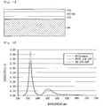
- FIG. 12 illustrates a graph in which light intensities of light-emitting diode packages for each wavelength depending on the presence of the air gap between the encapsulation layer and the light conversion plate are measured.
- a light-emitting diode package using a blue light-emitting diode chip and containing a green light-emitting phosphor in the encapsulation layer and a light conversion plate including red quantum dots were used, and the light intensity of the light-emitting diode package (reference), in which the light conversion plate is not stacked, for each wavelength was also measured for comparison.
- the light intensity of the light-emitting diode package reference
- a luminous efficiency of the light-emitting diode package, in which the light conversion plate was not stacked was denoted as 100%
- a luminous efficiency of the light-emitting diode package, in which the light conversion plate was stacked with the air gap was about 94%
- a luminous efficiency of the light-emitting diode package, in which the light conversion plate was directly stacked without the air gap was about 72%.
- a low refractive index layer having a refractive index of 1.3 to 1.4 was formed between the encapsulation layer and the light conversion plate, a luminous efficiency of about 80% to about 85% was obtained.
- the package body 20, as illustrated in FIG. 8 can be processed so that inner side surfaces thereof have two steps.
- the step formed on a side relatively close to the bottom surface of the package body is denoted as the first step 26, and the step formed on a side relatively far from the bottom surface is denoted as the second step 28.
- the air gap 50 or a low refractive index layer may also be disposed in a space formed by the first step 26, and the light conversion plate 10 may be inserted into a space which is formed by the second step 28.
- the light conversion plate 10 and the light-emitting diode package can be accurately aligned by a simple method.
- a side portion of the light conversion plate 10 is coated with a sealant 80 and the sealant 80 is then cured by UV curing so that the light conversion plate 10 may be fixed to the light-emitting diode package.
- the backlight unit 200 of an embodiment of the present disclosure uses the first embodiment of a light-emitting diode package of the present disclosure falling under the claimed invention as a light source.
- the backlight unit may be an edge type backlight unit or a direct type backlight unit.
- the edge type backlight unit of the embodiment of the present disclosure will be described with reference to FIG. 9 . As illustrated in FIG.
- the edge type backlight unit of the embodiment of the present disclosure includes a light guide plate 230, a light source unit which is disposed on at least one side of the light guide plate 230 and includes the first embodiment of a light-emitting diode package of the present disclosure falling under the claimed invention as a light source, a reflection member 220 disposed under the light guide plate 230, and an optical film 240 disposed on the light guide plate 230.
- the light source unit includes a plurality of light sources and a printed circuit board 110 on which the plurality of light sources is mounted.
- each light source is composed of the first embodiment of a light-emitting diode package of the present disclosure falling under the claimed invention. Because the light-emitting diode package has been already described, the detailed description thereof will be omitted.
- the light sources are mounted on the printed circuit board 110 and can be driven by a driving signal supplied through the printed circuit board.
- the light source unit is disposed on a side of the light guide plate 230.
- the light guide plate 230 functions to uniformly guide light provided from each light source to a display panel through total reflection, refraction, and scattering.
- the shape of the light guide plate 230 is not limited thereto.
- a thickness of the light guide plate 230 may be formed so the center is thinner than both sides of the light guide plate 230 so as to reduce a total thickness of the backlight unit 200, and the thickness of the light guide plate 230 may be formed to gradually decrease from the light source unit.
- one surface of the light guide plate 230 may include a pattern having a specific shape.
- the light guide plate 230 may include various patterns, such as an elliptical pattern, a polygon pattern, and a hologram pattern, to guide the light incident on the inside of the light guide plate 230.
- FIG. 9 illustrates the light source unit is disposed on one side of the light guide plate 230, the embodiment of the present disclosure is not limited thereto. That is, the light source unit may be disposed at both sides of the light guide plate 230.
- the reflection member 220 functions to increase the luminous efficiency by reflecting light emitted from the bottom of the light guide plate 230 to reenter into the light guide plate 230, where the reflection member 220 is disposed under the light guide plate 230.
- Reflection members well known in the art may be used as the reflection member 220 without restriction, and, for example, a metallic reflection sheet may be used.
- the optical film 240 may include a diffuser sheet 242 for improving light uniformity by diffusing the light emitted from the light guide plate, or condensing sheets 244 for improving front brightness by aligning the light in a specific direction.
- the condensing sheet include a prism sheet, a lenticular sheet, and a DBEF film. Appropriate sheets may be combined and used as the optical film according to the required optical properties.
- the light source unit, the light guide plate, and the optical films may be disposed and accommodated in a bottom case.
- the direct type backlight unit 200 of the embodiment of the present disclosure includes a diffuser plate 241, a light source unit which is disposed under the diffuser plate 241 and includes the first embodiment of a light-emitting diode package of the present disclosure falling under the claimed invention as a light source, an optical film 240 disposed on the diffuser plate 241, and a reflection member 220 disposed under the light source unit.
- the light source unit includes a plurality of light sources and a printed circuit board 110 on which the plurality of light sources is mounted.
- Each light source is composed of the first embodiment of a light-emitting diode package of the present disclosure falling under the claimed invention.
- the light source unit is disposed under the diffuser plate 241 in the direct type backlight unit.
- the diffuser plate 241 is an optical member for concealing the light source and improving the luminous efficiency by diffusing the light emitted from the light source unit.
- the optical film 240 for improving optical properties and brightness is disposed on the diffuser plate 241.
- the above-described diffuser sheet and/or condensing sheets may be used as the optical film 240.
- the reflection member 220 is for improving light-use efficiency by reflecting the light emitted toward the bottom of the backlight unit to proceed toward the display panel, wherein the reflection member 220 is disposed under the light source unit.
- Reflection members well known in the art may be used as the reflection member 220 without restriction, and, for example, a metallic reflection sheet may be used.
- the light source unit, the diffuser plate, and the optical film may be disposed and accommodated in a bottom case.
- the display device of the embodiment of the present disclosure includes a backlight unit 200 and a display panel 300 disposed on the backlight unit 200.
- the backlight unit 200 is the same as the above-described backlight unit 200 of the present disclosure, only the display panel 300 will be described below.
- the display panel 300 may be a liquid crystal display panel (LCD).
- the display panel 300 includes an upper substrate 330, a lower substrate 310 disposed to be spaced apart from the upper substrate 330, and a liquid crystal layer 320 sandwiched between the upper substrate 330 and the lower substrate 310.
- an upper polarizing plate and a lower polarizing plate for selectively transmitting specific polarized light are respectively disposed on a top surface of the upper substrate 330 and a bottom surface of the lower substrate 310.
- the display panel is divided into a display area and a non-display area.
- a gate line and a data line are disposed on one surface of the lower substrate 310.
- the gate line and the data line perpendicularly cross each other having a gate dielectric layer disposed therebetween to define a pixel area.
- the lower substrate 310 may be a thin film transistor substrate.
- a thin film transistor is disposed in the area, in which the gate line and the data line cross each other, on the one surface of the lower substrate 310. That is, the thin film transistor is included in the pixel area.
- a pixel electrode is disposed in each pixel area on the one surface of the lower substrate 310. The thin film transistor and the pixel electrode are electrically connected to each other.
- the thin film transistor is composed of a gate electrode, a semiconductor layer, a source electrode, and a drain electrode.
- the gate electrode may be formed by branching from the gate line.
- the source electrode may be formed by branching from the data line.
- the pixel electrode may be electrically connected to the drain electrode of the thin film transistor.
- the thin film transistor may be formed in a bottom gate structure, a top gate structure, or a double gate structure. That is, with respect to the thin film transistor, various changes and modifications may be made in the configuration of the thin film transistor without departing from the scope of the embodiment of the present disclosure.
- the upper substrate 330 may be a color filter substrate.
- the upper substrate 330 may include a red color filter, a green color filter, and a blue color filter which are alternatingly disposed to correspond to each pixel area in the grid.
- the display panel 300 includes a common electrode forming an electric field with the pixel electrode to drive the liquid crystal layer.
- a method of controlling the arrangement of liquid crystal molecules may include a twisted nematic (TN) mode, a vertical alignment (VA) mode, an in plane switching (IPS) mode, or a fringe field switching (FFS) mode.
- the common electrode may be disposed on the upper substrate 330 or the lower substrate 310 according to the method of controlling the arrangement of the liquid crystal molecules.
- the display panel 300 may have a different structure in addition to the structure illustrated in FIG. 11 .
- the above display panel may be a display panel having a color filter on transistor (COT) structure in which a thin film transistor, a color filter, and a black matrix are formed on a lower substrate.
- a protective layer may be formed between the thin film transistor and the color filter.
- a pixel electrode in contact with the thin film transistor is disposed on the lower substrate.
- the black matrix may be omitted to improve an aperture ratio and simplify a mask process, and the common electrode may be formed so as to also play a role of the black matrix.
- the display panel 300 is connected to a driving circuit unit for supplying a driving signal from the outside.
- the driving circuit unit may be mounted on the substrate of the display panel 300 or may be connected to the display panel 300 through a connecting member such as a tape carrier package.
- a light conversion plate of the present disclosure may effectively prevent the degradation of quantum dots. Also, because a protrusion pattern is formed on a surface of a glass substrate, the light conversion plate of the present disclosure minimizes reflection at the surface of the glass substrate and maximizes light extraction performance. Thus, a luminous efficiency of a light-emitting diode package may be improved.
- the light-emitting diode package of the present disclosure improves the efficiency of the light-emitting diode package and obtains high-quality white light.
Landscapes
- Physics & Mathematics (AREA)
- Nonlinear Science (AREA)
- Optics & Photonics (AREA)
- General Physics & Mathematics (AREA)
- Crystallography & Structural Chemistry (AREA)
- Chemical & Material Sciences (AREA)
- Mathematical Physics (AREA)
- Engineering & Computer Science (AREA)
- General Engineering & Computer Science (AREA)
- Spectroscopy & Molecular Physics (AREA)
- Microelectronics & Electronic Packaging (AREA)
- Planar Illumination Modules (AREA)
- Led Device Packages (AREA)
Claims (5)
- Lichtemittierendes Diodenpaket (100) umfassend:einen Paketkörper (20) mit einer Nut mit inneren Seitenflächen (22) und einer Bodenfläche (24);einen lichtemittierenden Diodenchip (30), der auf der Bodenfläche (24) des Paketkörpers (20) angebracht ist;eine Einkapselungsschicht (40), die den lichtemittierenden Diodenchip (30) abdichtet;eine Lichtumwandlungsplatte (10), die sowohl auf dem Paketkörper (20) als auch auf der Einkapselungsschicht (40) angeordnet ist; undeinen Luftspalt (50), der zwischen der Einkapselungsschicht (40) und der Lichtumwandlungsplatte (10) angeordnet ist,wobei die Lichtumwandlungsplatte (10) umfasst:ein erstes Glassubstrat (11),eine Lichtumwandlungsschicht (13), die auf dem ersten Glassubstrat (11) angeordnet ist und Quantenpunkte (17) enthält, die einfallendes Licht in Licht mit einem bestimmten Wellenlängenbereich umwandeln, undein zweites Glassubstrat (15), das auf der Lichtumwandlungsschicht (13) angeordnet ist,dadurch gekennzeichnet, dassein Vorsprungsmuster (11a, 15a) auf einer Oberfläche des ersten Glassubstrats (11), auf einer Oberfläche des zweiten Glassubstrats (15) oder auf einer Oberfläche sowohl des ersten Glassubstrats (11) als auch des zweiten Glassubstrats (15) gebildet ist und dass mindestens ein Abstandshalter (60) zwischen dem Paketkörper (20) und der Lichtumwandlungsplatte (10) angeordnet ist, wobei der mindestens eine Abstandshalter (60) den Luftspalt (50) zwischen der Einkapselungsschicht (40) und der Lichtumwandlungsplatte (10) bildet.
- Rückbeleuchtungseinheit (200) umfassend:
das lichtemittierende Diodenpaket (100) nach Anspruch 1 als eine Lichtquelle;ein Reflexionselement (220), das eingerichtet ist, um von der Lichtquelle emittiertes Licht zu reflektieren; undeinen optischen Film (240), der über dem Reflexionselement (220) angeordnet ist. - Rückbeleuchtungseinheit (200) nach Anspruch 2, ferner umfassend:eine Lichtleiterplatte (230), die zwischen dem Reflexionselement (220) und dem optischen Film (240) angeordnet ist,wobei das lichtemittierendes Diodenpaket (100) an mindestens einer Seite der Lichtleiterplatte (230) angeordnet ist.
- Rückbeleuchtungseinheit (200) nach Anspruch 2, ferner umfassend:eine Diffusorplatte (241), die zwischen dem Reflexionselement (220) und dem optischen Film (240) angeordnet ist,wobei das lichtemittierendes Diodenpaket (101) zwischen dem Reflexionselement (220) und der Diffusorplatte (241) angeordnet ist.
- Anzeigevorrichtung umfassend:die Rückbeleuchtungseinheit (200) nach einem der Ansprüche 2 bis 4; undeine Anzeigetafel (300), die auf der Rückbeleuchtungseinheit (200) angeordnet ist.
Applications Claiming Priority (1)
| Application Number | Priority Date | Filing Date | Title |
|---|---|---|---|
| KR1020150061284A KR101686737B1 (ko) | 2015-04-30 | 2015-04-30 | 광 변환 플레이트, 이를 포함하는 발광 다이오드 패키지, 백라이트 유닛 및 표시장치 |
Publications (2)
| Publication Number | Publication Date |
|---|---|
| EP3088950A1 EP3088950A1 (de) | 2016-11-02 |
| EP3088950B1 true EP3088950B1 (de) | 2021-02-24 |
Family
ID=54324779
Family Applications (1)
| Application Number | Title | Priority Date | Filing Date |
|---|---|---|---|
| EP15002904.9A Active EP3088950B1 (de) | 2015-04-30 | 2015-10-12 | Lichtemittierendes diodenpaket, rückbeleuchtungseinheit, und anzeigevorrichtung mit einer lichtumwandlungsplatte |
Country Status (4)
| Country | Link |
|---|---|
| US (1) | US9773955B2 (de) |
| EP (1) | EP3088950B1 (de) |
| KR (1) | KR101686737B1 (de) |
| CN (1) | CN106094328B (de) |
Cited By (1)
| Publication number | Priority date | Publication date | Assignee | Title |
|---|---|---|---|---|
| PL423437A1 (pl) * | 2017-11-13 | 2019-05-20 | Ml System Spolka Akcyjna | Sposób wytwarzania płyty szklanej świetlnej emitującej fale elektromagnetyczne i płyta szklana wytwarzana tym sposobem |
Families Citing this family (36)
| Publication number | Priority date | Publication date | Assignee | Title |
|---|---|---|---|---|
| CN105140377A (zh) * | 2015-08-10 | 2015-12-09 | 深圳市华星光电技术有限公司 | 量子点玻璃盒及其制备方法和应用 |
| CN105867026A (zh) * | 2016-06-03 | 2016-08-17 | 青岛海信电器股份有限公司 | 量子点光源器件、背光模组及液晶显示装置 |
| JP6665701B2 (ja) * | 2016-06-17 | 2020-03-13 | 日本電気硝子株式会社 | 波長変換部材及びその製造方法、並びに発光デバイス |
| CN106200118B (zh) * | 2016-07-06 | 2020-03-31 | 青岛海信电器股份有限公司 | 量子点光源组件、背光模组及液晶显示装置 |
| KR102793985B1 (ko) | 2016-12-05 | 2025-04-15 | 삼성디스플레이 주식회사 | 포토루미네센스 장치 및 그것을 포함하는 디스플레이 패널 |
| JP7057486B2 (ja) * | 2016-12-27 | 2022-04-20 | 日亜化学工業株式会社 | 光源装置 |
| US10955607B2 (en) * | 2017-03-07 | 2021-03-23 | Lumileds Llc | LED lighting device with remote phosphor in-coupling structure for in-coupling light from light emitting diodes |
| CN114624806B (zh) * | 2017-06-30 | 2024-10-29 | 日亚化学工业株式会社 | 发光模块 |
| CN107238886A (zh) * | 2017-07-07 | 2017-10-10 | 青岛骐骥光电科技有限公司 | 一种玻璃导光板及其制作方法 |
| JP7090842B2 (ja) * | 2017-07-27 | 2022-06-27 | 日本電気硝子株式会社 | 波長変換部材及び発光装置 |
| KR102446538B1 (ko) * | 2017-08-16 | 2022-09-26 | 삼성디스플레이 주식회사 | 백라이트 유닛, 표시 장치 및 표시 장치의 제조 방법 |
| KR102459728B1 (ko) * | 2017-10-20 | 2022-10-31 | 삼성디스플레이 주식회사 | 액정 표시 패널 및 이를 포함하는 액정 표시 장치 |
| KR20190081087A (ko) * | 2017-12-29 | 2019-07-09 | 주식회사 루멘스 | 발광소자 |
| KR102485577B1 (ko) * | 2018-01-08 | 2023-01-09 | 삼성디스플레이 주식회사 | 백라이트 유닛 및 이를 포함하는 표시 장치 |
| US10256376B1 (en) * | 2018-01-16 | 2019-04-09 | Leedarson Lighting Co. Ltd. | LED device |
| US10069047B1 (en) * | 2018-01-16 | 2018-09-04 | Leedarson Lighting Co. Ltd. | LED device |
| US20190219874A1 (en) * | 2018-01-16 | 2019-07-18 | Huizhou China Star Optoelectronics Technology Co., Ltd. | Backlight module and display device |
| CN207834349U (zh) | 2018-01-16 | 2018-09-07 | 漳州立达信光电子科技有限公司 | 一种led封装结构 |
| US10243116B1 (en) * | 2018-01-16 | 2019-03-26 | Leedarson Lighting Co. Ltd. | LED device |
| TWI672834B (zh) * | 2018-01-25 | 2019-09-21 | Primax Electronics Ltd. | 光源模組以及光源模組之製造方法 |
| CN110346859B (zh) * | 2018-04-08 | 2023-05-16 | 京东方科技集团股份有限公司 | 光学谐振腔、显示面板 |
| KR102723985B1 (ko) * | 2018-07-27 | 2024-10-31 | 삼성전자주식회사 | 디스플레이 장치 |
| KR102593215B1 (ko) * | 2018-10-25 | 2023-10-25 | 삼성디스플레이 주식회사 | 표시장치 |
| CN111458925A (zh) * | 2019-01-18 | 2020-07-28 | 中强光电股份有限公司 | 光源模块及显示装置 |
| CN109686835A (zh) * | 2019-01-28 | 2019-04-26 | 深圳市领德奥普电子有限公司 | 一种led灯的uvc封装结构及其制备方法 |
| KR102719745B1 (ko) * | 2019-02-01 | 2024-10-18 | 삼성디스플레이 주식회사 | 표시 장치 및 그 제조 방법 |
| KR102592685B1 (ko) * | 2019-03-05 | 2023-10-23 | 삼성디스플레이 주식회사 | 백라이트 유닛 및 이를 포함하는 표시 장치 |
| KR102792752B1 (ko) * | 2019-05-08 | 2025-04-07 | 소에이 가가쿠 고교 가부시키가이샤 | 광 추출 효율이 개선된 나노구조체 기반 디스플레이 디바이스들 |
| EP4106117A4 (de) * | 2020-02-13 | 2024-03-13 | Nichia Corporation | Lichtemissionsmodul |
| US11921311B2 (en) | 2020-03-27 | 2024-03-05 | Nitto Denko Corporation | Illumination device |
| CN111725376A (zh) * | 2020-06-20 | 2020-09-29 | 广州市鸿利显示电子有限公司 | 一种光源组件制备方法 |
| EP4071809A1 (de) * | 2021-04-07 | 2022-10-12 | Samsung Electronics Co., Ltd. | Farbumwandlungsstruktur, anzeigevorrichtung und verfahren zur herstellung der anzeigevorrichtung |
| CN113703226B (zh) * | 2021-09-08 | 2022-09-27 | 广东粤港澳大湾区国家纳米科技创新研究院 | 高亮度、防蓝光量子点光学板及其制备方法和背光模组 |
| CN115657169B (zh) * | 2022-11-17 | 2025-06-27 | 南通惟怡新材料科技有限公司 | 量子点透镜、背光模组、显示装置及量子点透镜制作方法 |
| CN115963663B (zh) * | 2022-12-29 | 2024-11-22 | 深圳创维-Rgb电子有限公司 | 背光模组及显示装置 |
| WO2026005878A1 (en) * | 2024-06-24 | 2026-01-02 | Dstar Communications, Inc. | High density interconnects with 3d broadband electrooptic infrared components |
Citations (2)
| Publication number | Priority date | Publication date | Assignee | Title |
|---|---|---|---|---|
| CN103672609A (zh) * | 2013-12-02 | 2014-03-26 | 深圳市华星光电技术有限公司 | 使用量子点的发光源及其制作方法与应用 |
| EP2843717A1 (de) * | 2013-08-27 | 2015-03-04 | Industry-Academic Cooperation Foundation Yonsei University | Phosphorschicht und lichtemittierende Vorrichtung und System damit |
Family Cites Families (15)
| Publication number | Priority date | Publication date | Assignee | Title |
|---|---|---|---|---|
| JPH10125463A (ja) * | 1995-12-28 | 1998-05-15 | Matsushita Electric Ind Co Ltd | 有機エレクトロルミネセンス素子、液晶照明装置、表示デバイス装置、および、有機エレクトロルミネセンス素子の製造方法 |
| KR20060087313A (ko) * | 2005-01-29 | 2006-08-02 | 삼성전자주식회사 | 나노 복합 재료 및 그 제조 방법 |
| KR100682874B1 (ko) * | 2005-05-02 | 2007-02-15 | 삼성전기주식회사 | 백색 led |
| CN1956231A (zh) * | 2005-10-28 | 2007-05-02 | 财团法人工业技术研究院 | 偏极化发光元件 |
| JP2007194675A (ja) | 2007-04-26 | 2007-08-02 | Kyocera Corp | 発光装置 |
| JP2013509714A (ja) * | 2009-10-30 | 2013-03-14 | ナノシス・インク. | ナノ結晶を含む発光ダイオード(led)デバイス |
| KR101210158B1 (ko) | 2010-11-04 | 2012-12-07 | 엘지이노텍 주식회사 | 표시장치 및 광 변환 부재 |
| KR102496406B1 (ko) * | 2010-11-10 | 2023-02-06 | 나노시스, 인크. | 양자 도트 필름들, 조명 디바이스들, 및 조명 방법들 |
| KR101210066B1 (ko) * | 2011-01-31 | 2012-12-07 | 엘지이노텍 주식회사 | 광 변환 부재 및 이를 포함하는 표시장치 |
| KR101221921B1 (ko) | 2011-07-05 | 2013-01-15 | 엘지전자 주식회사 | 이동 단말기 |
| KR20130015847A (ko) * | 2011-08-05 | 2013-02-14 | 삼성전자주식회사 | 발광장치, 백라이트 유닛과 디스플레이 장치 및 그 제조방법 |
| KR20130084506A (ko) | 2012-01-17 | 2013-07-25 | 삼성전자주식회사 | 발광소자 패키지 및 그 제조방법 |
| KR101382974B1 (ko) * | 2012-03-30 | 2014-04-08 | 엘지이노텍 주식회사 | 광 변환 복합체, 이를 포함하는 발광장치 및 표시장치 및 이의 제조방법 |
| KR102062687B1 (ko) * | 2013-01-23 | 2020-01-06 | 엘지전자 주식회사 | 양자점 복합 필름 및 이를 이용한 백라이트 유닛 |
| KR102084039B1 (ko) | 2013-07-02 | 2020-03-04 | 삼성디스플레이 주식회사 | 광원 유닛, 그것의 제조 방법, 및 그것을 포함하는 백라이트 유닛 |
-
2015
- 2015-04-30 KR KR1020150061284A patent/KR101686737B1/ko active Active
- 2015-10-12 EP EP15002904.9A patent/EP3088950B1/de active Active
- 2015-10-16 US US14/885,478 patent/US9773955B2/en active Active
- 2015-11-10 CN CN201510761217.9A patent/CN106094328B/zh active Active
Patent Citations (3)
| Publication number | Priority date | Publication date | Assignee | Title |
|---|---|---|---|---|
| EP2843717A1 (de) * | 2013-08-27 | 2015-03-04 | Industry-Academic Cooperation Foundation Yonsei University | Phosphorschicht und lichtemittierende Vorrichtung und System damit |
| CN103672609A (zh) * | 2013-12-02 | 2014-03-26 | 深圳市华星光电技术有限公司 | 使用量子点的发光源及其制作方法与应用 |
| US20150311385A1 (en) * | 2013-12-02 | 2015-10-29 | Shenzhen China Star Optoelectronics Technology Co., Ltd. | Luminous Source Utilizing Quantum Dot, and Its Manufacturing Method and Application |
Cited By (1)
| Publication number | Priority date | Publication date | Assignee | Title |
|---|---|---|---|---|
| PL423437A1 (pl) * | 2017-11-13 | 2019-05-20 | Ml System Spolka Akcyjna | Sposób wytwarzania płyty szklanej świetlnej emitującej fale elektromagnetyczne i płyta szklana wytwarzana tym sposobem |
Also Published As
| Publication number | Publication date |
|---|---|
| KR20160129328A (ko) | 2016-11-09 |
| US9773955B2 (en) | 2017-09-26 |
| CN106094328B (zh) | 2019-07-16 |
| KR101686737B1 (ko) | 2016-12-14 |
| CN106094328A (zh) | 2016-11-09 |
| US20160322543A1 (en) | 2016-11-03 |
| EP3088950A1 (de) | 2016-11-02 |
Similar Documents
| Publication | Publication Date | Title |
|---|---|---|
| EP3088950B1 (de) | Lichtemittierendes diodenpaket, rückbeleuchtungseinheit, und anzeigevorrichtung mit einer lichtumwandlungsplatte | |
| KR101604339B1 (ko) | 광 변환 필름, 이를 포함하는 백라이트 유닛 및 표시장치 | |
| KR101851726B1 (ko) | 표시장치 | |
| EP3053874B1 (de) | Lichtumwandlungselement und rückbeleuchtungseinheit und anzeigevorrichtung damit | |
| CN106200109B (zh) | 光转换构件、背光单元和包括它们的显示设备 | |
| KR101778848B1 (ko) | 발광소자 패키지 어셈블리 및 이의 제조 방법 | |
| KR101786097B1 (ko) | 광학 부재, 이를 포함하는 표시장치 및 이의 제조방법 | |
| US10056529B2 (en) | Photo-conversion complex, and photo-conversion member, display device, and light-emitting device package including the same, and method of fabricating the same | |
| EP2771737B1 (de) | Optisches element | |
| US9447932B2 (en) | Light-emitting diode package and method of manufacturing the same | |
| KR20160123838A (ko) | 양자점-고분자 복합체의 제조 방법, 양자점-고분자 복합체, 이를 포함하는 광 변환 필름, 백라이트 유닛 및 표시장치 | |
| KR101870443B1 (ko) | 광학 부재 및 이를 포함하는 표시장치 | |
| KR101778864B1 (ko) | 광 변환 부재 및 이를 포함하는 표시장치 및 발광소자 패키지 | |
| KR101862873B1 (ko) | 광학 부재, 발광장치 및 표시장치 | |
| KR102310178B1 (ko) | 백라이트 유닛 및 이를 포함하는 표시 장치 | |
| KR101934419B1 (ko) | 광 변환 복합체, 이를 포함하는 발광장치 및 표시장치 및 이의 제조방법 | |
| KR101877485B1 (ko) | 광 변환 부재, 이를 포함하는 발광장치 및 표시장치 | |
| KR101349426B1 (ko) | 광학 부재 및 표시장치 | |
| KR101327027B1 (ko) | 광 변환 복합체, 이를 포함하는 발광장치 및 표시장치 및 이의 제조방법 | |
| KR20130068649A (ko) | 광학 부재, 이를 포함하는 발광장치 및 표시장치 및 이의 제조방법 |
Legal Events
| Date | Code | Title | Description |
|---|---|---|---|
| PUAI | Public reference made under article 153(3) epc to a published international application that has entered the european phase |
Free format text: ORIGINAL CODE: 0009012 |
|
| 17P | Request for examination filed |
Effective date: 20160513 |
|
| AK | Designated contracting states |
Kind code of ref document: A1 Designated state(s): AL AT BE BG CH CY CZ DE DK EE ES FI FR GB GR HR HU IE IS IT LI LT LU LV MC MK MT NL NO PL PT RO RS SE SI SK SM TR |
|
| AX | Request for extension of the european patent |
Extension state: BA ME |
|
| STAA | Information on the status of an ep patent application or granted ep patent |
Free format text: STATUS: EXAMINATION IS IN PROGRESS |
|
| 17Q | First examination report despatched |
Effective date: 20200330 |
|
| REG | Reference to a national code |
Ref country code: DE Ref legal event code: R079 Ref document number: 602015065901 Country of ref document: DE Free format text: PREVIOUS MAIN CLASS: G02F0001133570 Ipc: F21V0009320000 |
|
| GRAP | Despatch of communication of intention to grant a patent |
Free format text: ORIGINAL CODE: EPIDOSNIGR1 |
|
| STAA | Information on the status of an ep patent application or granted ep patent |
Free format text: STATUS: GRANT OF PATENT IS INTENDED |
|
| RIC1 | Information provided on ipc code assigned before grant |
Ipc: F21V 13/14 20060101ALI20200909BHEP Ipc: H01L 33/50 20100101ALI20200909BHEP Ipc: G02F 2/02 20060101ALI20200909BHEP Ipc: H01L 33/52 20100101ALN20200909BHEP Ipc: G02F 1/13357 20060101ALI20200909BHEP Ipc: F21V 9/32 20180101AFI20200909BHEP Ipc: H01L 33/48 20100101ALN20200909BHEP |
|
| INTG | Intention to grant announced |
Effective date: 20200928 |
|
| RIN1 | Information on inventor provided before grant (corrected) |
Inventor name: JEON, SEONGMAN Inventor name: OH, JINMOK Inventor name: SHIN, HYUNKWON Inventor name: SUNG, JINWOO |
|
| GRAS | Grant fee paid |
Free format text: ORIGINAL CODE: EPIDOSNIGR3 |
|
| GRAA | (expected) grant |
Free format text: ORIGINAL CODE: 0009210 |
|
| STAA | Information on the status of an ep patent application or granted ep patent |
Free format text: STATUS: THE PATENT HAS BEEN GRANTED |
|
| AK | Designated contracting states |
Kind code of ref document: B1 Designated state(s): AL AT BE BG CH CY CZ DE DK EE ES FI FR GB GR HR HU IE IS IT LI LT LU LV MC MK MT NL NO PL PT RO RS SE SI SK SM TR |
|
| REG | Reference to a national code |
Ref country code: GB Ref legal event code: FG4D |
|
| REG | Reference to a national code |
Ref country code: CH Ref legal event code: EP |
|
| REG | Reference to a national code |
Ref country code: DE Ref legal event code: R096 Ref document number: 602015065901 Country of ref document: DE |
|
| REG | Reference to a national code |
Ref country code: AT Ref legal event code: REF Ref document number: 1364910 Country of ref document: AT Kind code of ref document: T Effective date: 20210315 |
|
| REG | Reference to a national code |
Ref country code: IE Ref legal event code: FG4D |
|
| REG | Reference to a national code |
Ref country code: LT Ref legal event code: MG9D |
|
| REG | Reference to a national code |
Ref country code: NL Ref legal event code: MP Effective date: 20210224 |
|
| PG25 | Lapsed in a contracting state [announced via postgrant information from national office to epo] |
Ref country code: PT Free format text: LAPSE BECAUSE OF FAILURE TO SUBMIT A TRANSLATION OF THE DESCRIPTION OR TO PAY THE FEE WITHIN THE PRESCRIBED TIME-LIMIT Effective date: 20210624 Ref country code: LT Free format text: LAPSE BECAUSE OF FAILURE TO SUBMIT A TRANSLATION OF THE DESCRIPTION OR TO PAY THE FEE WITHIN THE PRESCRIBED TIME-LIMIT Effective date: 20210224 Ref country code: GR Free format text: LAPSE BECAUSE OF FAILURE TO SUBMIT A TRANSLATION OF THE DESCRIPTION OR TO PAY THE FEE WITHIN THE PRESCRIBED TIME-LIMIT Effective date: 20210525 Ref country code: HR Free format text: LAPSE BECAUSE OF FAILURE TO SUBMIT A TRANSLATION OF THE DESCRIPTION OR TO PAY THE FEE WITHIN THE PRESCRIBED TIME-LIMIT Effective date: 20210224 Ref country code: FI Free format text: LAPSE BECAUSE OF FAILURE TO SUBMIT A TRANSLATION OF THE DESCRIPTION OR TO PAY THE FEE WITHIN THE PRESCRIBED TIME-LIMIT Effective date: 20210224 Ref country code: BG Free format text: LAPSE BECAUSE OF FAILURE TO SUBMIT A TRANSLATION OF THE DESCRIPTION OR TO PAY THE FEE WITHIN THE PRESCRIBED TIME-LIMIT Effective date: 20210524 Ref country code: NO Free format text: LAPSE BECAUSE OF FAILURE TO SUBMIT A TRANSLATION OF THE DESCRIPTION OR TO PAY THE FEE WITHIN THE PRESCRIBED TIME-LIMIT Effective date: 20210524 |
|
| REG | Reference to a national code |
Ref country code: AT Ref legal event code: MK05 Ref document number: 1364910 Country of ref document: AT Kind code of ref document: T Effective date: 20210224 |
|
| PG25 | Lapsed in a contracting state [announced via postgrant information from national office to epo] |
Ref country code: SE Free format text: LAPSE BECAUSE OF FAILURE TO SUBMIT A TRANSLATION OF THE DESCRIPTION OR TO PAY THE FEE WITHIN THE PRESCRIBED TIME-LIMIT Effective date: 20210224 Ref country code: RS Free format text: LAPSE BECAUSE OF FAILURE TO SUBMIT A TRANSLATION OF THE DESCRIPTION OR TO PAY THE FEE WITHIN THE PRESCRIBED TIME-LIMIT Effective date: 20210224 Ref country code: NL Free format text: LAPSE BECAUSE OF FAILURE TO SUBMIT A TRANSLATION OF THE DESCRIPTION OR TO PAY THE FEE WITHIN THE PRESCRIBED TIME-LIMIT Effective date: 20210224 Ref country code: LV Free format text: LAPSE BECAUSE OF FAILURE TO SUBMIT A TRANSLATION OF THE DESCRIPTION OR TO PAY THE FEE WITHIN THE PRESCRIBED TIME-LIMIT Effective date: 20210224 Ref country code: PL Free format text: LAPSE BECAUSE OF FAILURE TO SUBMIT A TRANSLATION OF THE DESCRIPTION OR TO PAY THE FEE WITHIN THE PRESCRIBED TIME-LIMIT Effective date: 20210224 |
|
| PG25 | Lapsed in a contracting state [announced via postgrant information from national office to epo] |
Ref country code: IS Free format text: LAPSE BECAUSE OF FAILURE TO SUBMIT A TRANSLATION OF THE DESCRIPTION OR TO PAY THE FEE WITHIN THE PRESCRIBED TIME-LIMIT Effective date: 20210624 |
|
| PG25 | Lapsed in a contracting state [announced via postgrant information from national office to epo] |
Ref country code: CZ Free format text: LAPSE BECAUSE OF FAILURE TO SUBMIT A TRANSLATION OF THE DESCRIPTION OR TO PAY THE FEE WITHIN THE PRESCRIBED TIME-LIMIT Effective date: 20210224 Ref country code: EE Free format text: LAPSE BECAUSE OF FAILURE TO SUBMIT A TRANSLATION OF THE DESCRIPTION OR TO PAY THE FEE WITHIN THE PRESCRIBED TIME-LIMIT Effective date: 20210224 Ref country code: AT Free format text: LAPSE BECAUSE OF FAILURE TO SUBMIT A TRANSLATION OF THE DESCRIPTION OR TO PAY THE FEE WITHIN THE PRESCRIBED TIME-LIMIT Effective date: 20210224 Ref country code: SM Free format text: LAPSE BECAUSE OF FAILURE TO SUBMIT A TRANSLATION OF THE DESCRIPTION OR TO PAY THE FEE WITHIN THE PRESCRIBED TIME-LIMIT Effective date: 20210224 |
|
| REG | Reference to a national code |
Ref country code: DE Ref legal event code: R097 Ref document number: 602015065901 Country of ref document: DE |
|
| PG25 | Lapsed in a contracting state [announced via postgrant information from national office to epo] |
Ref country code: ES Free format text: LAPSE BECAUSE OF FAILURE TO SUBMIT A TRANSLATION OF THE DESCRIPTION OR TO PAY THE FEE WITHIN THE PRESCRIBED TIME-LIMIT Effective date: 20210224 Ref country code: DK Free format text: LAPSE BECAUSE OF FAILURE TO SUBMIT A TRANSLATION OF THE DESCRIPTION OR TO PAY THE FEE WITHIN THE PRESCRIBED TIME-LIMIT Effective date: 20210224 Ref country code: SK Free format text: LAPSE BECAUSE OF FAILURE TO SUBMIT A TRANSLATION OF THE DESCRIPTION OR TO PAY THE FEE WITHIN THE PRESCRIBED TIME-LIMIT Effective date: 20210224 Ref country code: RO Free format text: LAPSE BECAUSE OF FAILURE TO SUBMIT A TRANSLATION OF THE DESCRIPTION OR TO PAY THE FEE WITHIN THE PRESCRIBED TIME-LIMIT Effective date: 20210224 |
|
| PLBE | No opposition filed within time limit |
Free format text: ORIGINAL CODE: 0009261 |
|
| STAA | Information on the status of an ep patent application or granted ep patent |
Free format text: STATUS: NO OPPOSITION FILED WITHIN TIME LIMIT |
|
| PG25 | Lapsed in a contracting state [announced via postgrant information from national office to epo] |
Ref country code: AL Free format text: LAPSE BECAUSE OF FAILURE TO SUBMIT A TRANSLATION OF THE DESCRIPTION OR TO PAY THE FEE WITHIN THE PRESCRIBED TIME-LIMIT Effective date: 20210224 |
|
| 26N | No opposition filed |
Effective date: 20211125 |
|
| PG25 | Lapsed in a contracting state [announced via postgrant information from national office to epo] |
Ref country code: SI Free format text: LAPSE BECAUSE OF FAILURE TO SUBMIT A TRANSLATION OF THE DESCRIPTION OR TO PAY THE FEE WITHIN THE PRESCRIBED TIME-LIMIT Effective date: 20210224 |
|
| PG25 | Lapsed in a contracting state [announced via postgrant information from national office to epo] |
Ref country code: IT Free format text: LAPSE BECAUSE OF FAILURE TO SUBMIT A TRANSLATION OF THE DESCRIPTION OR TO PAY THE FEE WITHIN THE PRESCRIBED TIME-LIMIT Effective date: 20210224 |
|
| REG | Reference to a national code |
Ref country code: CH Ref legal event code: PL |
|
| PG25 | Lapsed in a contracting state [announced via postgrant information from national office to epo] |
Ref country code: IS Free format text: LAPSE BECAUSE OF FAILURE TO SUBMIT A TRANSLATION OF THE DESCRIPTION OR TO PAY THE FEE WITHIN THE PRESCRIBED TIME-LIMIT Effective date: 20210624 |
|
| REG | Reference to a national code |
Ref country code: BE Ref legal event code: MM Effective date: 20211031 |
|
| GBPC | Gb: european patent ceased through non-payment of renewal fee |
Effective date: 20211012 |
|
| PG25 | Lapsed in a contracting state [announced via postgrant information from national office to epo] |
Ref country code: MC Free format text: LAPSE BECAUSE OF FAILURE TO SUBMIT A TRANSLATION OF THE DESCRIPTION OR TO PAY THE FEE WITHIN THE PRESCRIBED TIME-LIMIT Effective date: 20210224 |
|
| PG25 | Lapsed in a contracting state [announced via postgrant information from national office to epo] |
Ref country code: LU Free format text: LAPSE BECAUSE OF NON-PAYMENT OF DUE FEES Effective date: 20211012 Ref country code: GB Free format text: LAPSE BECAUSE OF NON-PAYMENT OF DUE FEES Effective date: 20211012 Ref country code: BE Free format text: LAPSE BECAUSE OF NON-PAYMENT OF DUE FEES Effective date: 20211031 |
|
| PG25 | Lapsed in a contracting state [announced via postgrant information from national office to epo] |
Ref country code: LI Free format text: LAPSE BECAUSE OF NON-PAYMENT OF DUE FEES Effective date: 20211031 Ref country code: CH Free format text: LAPSE BECAUSE OF NON-PAYMENT OF DUE FEES Effective date: 20211031 |
|
| PG25 | Lapsed in a contracting state [announced via postgrant information from national office to epo] |
Ref country code: FR Free format text: LAPSE BECAUSE OF NON-PAYMENT OF DUE FEES Effective date: 20211031 |
|
| PG25 | Lapsed in a contracting state [announced via postgrant information from national office to epo] |
Ref country code: IE Free format text: LAPSE BECAUSE OF NON-PAYMENT OF DUE FEES Effective date: 20211012 |
|
| PG25 | Lapsed in a contracting state [announced via postgrant information from national office to epo] |
Ref country code: HU Free format text: LAPSE BECAUSE OF FAILURE TO SUBMIT A TRANSLATION OF THE DESCRIPTION OR TO PAY THE FEE WITHIN THE PRESCRIBED TIME-LIMIT; INVALID AB INITIO Effective date: 20151012 |
|
| PG25 | Lapsed in a contracting state [announced via postgrant information from national office to epo] |
Ref country code: CY Free format text: LAPSE BECAUSE OF FAILURE TO SUBMIT A TRANSLATION OF THE DESCRIPTION OR TO PAY THE FEE WITHIN THE PRESCRIBED TIME-LIMIT Effective date: 20210224 |
|
| PG25 | Lapsed in a contracting state [announced via postgrant information from national office to epo] |
Ref country code: MK Free format text: LAPSE BECAUSE OF FAILURE TO SUBMIT A TRANSLATION OF THE DESCRIPTION OR TO PAY THE FEE WITHIN THE PRESCRIBED TIME-LIMIT Effective date: 20210224 |
|
| PG25 | Lapsed in a contracting state [announced via postgrant information from national office to epo] |
Ref country code: MT Free format text: LAPSE BECAUSE OF FAILURE TO SUBMIT A TRANSLATION OF THE DESCRIPTION OR TO PAY THE FEE WITHIN THE PRESCRIBED TIME-LIMIT Effective date: 20210224 |
|
| PG25 | Lapsed in a contracting state [announced via postgrant information from national office to epo] |
Ref country code: TR Free format text: LAPSE BECAUSE OF FAILURE TO SUBMIT A TRANSLATION OF THE DESCRIPTION OR TO PAY THE FEE WITHIN THE PRESCRIBED TIME-LIMIT Effective date: 20210224 |
|
| PGFP | Annual fee paid to national office [announced via postgrant information from national office to epo] |
Ref country code: DE Payment date: 20250908 Year of fee payment: 11 |