EP3089202A1 - Verfahren und vorrichtung form zur analyse der form eines wafers - Google Patents
Verfahren und vorrichtung form zur analyse der form eines wafers Download PDFInfo
- Publication number
- EP3089202A1 EP3089202A1 EP14875737.0A EP14875737A EP3089202A1 EP 3089202 A1 EP3089202 A1 EP 3089202A1 EP 14875737 A EP14875737 A EP 14875737A EP 3089202 A1 EP3089202 A1 EP 3089202A1
- Authority
- EP
- European Patent Office
- Prior art keywords
- wafer
- contour
- temporary
- coordinates
- pixels
- Prior art date
- Legal status (The legal status is an assumption and is not a legal conclusion. Google has not performed a legal analysis and makes no representation as to the accuracy of the status listed.)
- Granted
Links
Images



Classifications
-
- G—PHYSICS
- G06—COMPUTING OR CALCULATING; COUNTING
- G06T—IMAGE DATA PROCESSING OR GENERATION, IN GENERAL
- G06T7/00—Image analysis
- G06T7/0002—Inspection of images, e.g. flaw detection
- G06T7/0004—Industrial image inspection
- G06T7/0006—Industrial image inspection using a design-rule based approach
-
- H—ELECTRICITY
- H10—SEMICONDUCTOR DEVICES; ELECTRIC SOLID-STATE DEVICES NOT OTHERWISE PROVIDED FOR
- H10P—GENERIC PROCESSES OR APPARATUS FOR THE MANUFACTURE OR TREATMENT OF DEVICES COVERED BY CLASS H10
- H10P14/00—Formation of materials, e.g. in the shape of layers or pillars
- H10P14/20—Formation of materials, e.g. in the shape of layers or pillars of semiconductor materials
-
- G—PHYSICS
- G06—COMPUTING OR CALCULATING; COUNTING
- G06T—IMAGE DATA PROCESSING OR GENERATION, IN GENERAL
- G06T7/00—Image analysis
- G06T7/60—Analysis of geometric attributes
-
- H—ELECTRICITY
- H10—SEMICONDUCTOR DEVICES; ELECTRIC SOLID-STATE DEVICES NOT OTHERWISE PROVIDED FOR
- H10P—GENERIC PROCESSES OR APPARATUS FOR THE MANUFACTURE OR TREATMENT OF DEVICES COVERED BY CLASS H10
- H10P74/00—Testing or measuring during manufacture or treatment of wafers, substrates or devices
-
- H—ELECTRICITY
- H10—SEMICONDUCTOR DEVICES; ELECTRIC SOLID-STATE DEVICES NOT OTHERWISE PROVIDED FOR
- H10P—GENERIC PROCESSES OR APPARATUS FOR THE MANUFACTURE OR TREATMENT OF DEVICES COVERED BY CLASS H10
- H10P74/00—Testing or measuring during manufacture or treatment of wafers, substrates or devices
- H10P74/20—Testing or measuring during manufacture or treatment of wafers, substrates or devices characterised by the properties tested or measured, e.g. structural or electrical properties
- H10P74/203—Structural properties, e.g. testing or measuring thicknesses, line widths, warpage, bond strengths or physical defects
-
- G—PHYSICS
- G06—COMPUTING OR CALCULATING; COUNTING
- G06T—IMAGE DATA PROCESSING OR GENERATION, IN GENERAL
- G06T2207/00—Indexing scheme for image analysis or image enhancement
- G06T2207/10—Image acquisition modality
- G06T2207/10056—Microscopic image
- G06T2207/10061—Microscopic image from scanning electron microscope
-
- G—PHYSICS
- G06—COMPUTING OR CALCULATING; COUNTING
- G06T—IMAGE DATA PROCESSING OR GENERATION, IN GENERAL
- G06T2207/00—Indexing scheme for image analysis or image enhancement
- G06T2207/30—Subject of image; Context of image processing
- G06T2207/30108—Industrial image inspection
- G06T2207/30148—Semiconductor; IC; Wafer
Definitions
- the embodiment relates to a method and apparatus of analyzing a shape of a wafer.
- Semiconductor devices are formed on a wafer.
- an edge of the wafer in order to achieve high integration and high yields of the semiconductor devices, it is required for an edge of the wafer to have high purity and an appropriate shape suitable for a method of manufacturing the semiconductor device.
- a practical and easy method of analyzing a shape of an edge of a wafer is required.
- one of the most important mathematical parameters of the shape of the edge of the wafer is a curvature, and an overall curvature formed by the edge of the wafer and a front surface of the wafer should be as small as possible. This is because the front surface of the wafer and the edge of the wafer are smoothly formed without a boundary with each other when the curvature is small.
- the wafer may be non-uniformly coated with a photoresist (PR) and the like may occur in a process for manufacturing the semiconductor device on the wafer.
- PR photoresist
- the embodiment is directed to providing a method and apparatus of analyzing a shape of a wafer in which the shape of the wafer can be simply analyzed through an image processing technique without the aid of separate apparatuses such as a laser and the like.
- One aspect of the present invention provides a method of analyzing a shape of a wafer including acquiring a sectional image showing a wafer to be analyzed, finding a series of coordinates of a surface contour of the wafer in the sectional image, and obtaining shape analysis data including information on a shape of the wafer using the series of coordinates.
- the sectional image may show an edge of the wafer and an edge vicinity, and the shape of the wafer may include shapes of the edge and the edge vicinity.
- the acquiring of the sectional image may include capturing the edge and the edge vicinity of the wafer using an electron microscope.
- Each of a horizontal size and a vertical size of each pixel in the sectional image may be less than or equal to 1% of a size of the shape of the wafer. Further, each of the horizontal size and the vertical size of each of the pixels in the sectional image may be in a range of 0.25 ⁇ m to 2 ⁇ m.
- the acquiring of the sectional image may include acquiring a plurality of divided images by capturing the edge and the edge vicinity several times, and acquiring the sectional image by combining the plurality of divided images.
- the combining of the plurality of divided image may include analyzing a luminance of each of the plurality of divided images, overlapping intervals having a similar luminance, and acquiring the sectional image.
- the method of analyzing the shape of the wafer may further include increasing a contrast between the wafer and a periphery of the wafer in the sectional image, and the series of coordinates of the surface contour may be found in the sectional image in which the contrast is increased.
- the finding of the series of coordinates of the surface contour may include obtaining a luminance of each pixel in the sectional image, obtaining luminance differences between adjacent pixels, determining temporary contour pixels using the luminance differences, re-determining the temporary contour pixels when modification of a temporary surface contour formed by the temporary contour pixels is required, and determining an array of the temporary contour pixels as the series of coordinates of the surface contour when the modification of the temporary surface contour is not required.
- the determining of the temporary contour pixels may include finding the adjacent pixels showing a relatively large luminance difference among the luminance differences and determining the found adjacent pixels as the temporary contour pixels.
- the determining of the temporary contour pixels may include listing the luminance differences in order from largest to smallest and determining pixels showing top level luminance differences in all the listed luminance differences as the temporary contour pixels.
- the modification of the temporary surface contour may be required by an operator.
- the modification of the temporary surface contour may be determined to be required when an interval between the temporary contour pixels is out of a threshold distance.
- the threshold distance may be in a range of 1 pixel to 100 pixels.
- the threshold distance may be a distance within 10% of a distance from the temporary surface contour.
- the threshold distance may be a distance corresponding to 1% of a size of the shape of the wafer.
- the finding of the series of coordinates of the surface contour may further include converting the array of the temporary contour pixels determined as the series of coordinates of the surface contour into a series of coordinates having a form of Cartesian coordinates.
- the luminance difference may be determined as a relatively large luminance difference when the luminance difference is out of a threshold luminance range.
- the threshold luminance range may be in a range of a gray scale of 0.01 to a gray scale of 0.1.
- the obtaining of the shape analysis data may include smoothing a curve made of a series of discrete coordinates of the surface contour and calculating the shape analysis data using the smoothed curve.
- the shape analysis data may include a curvature formed by both of the edge and the edge vicinity.
- the shape analysis data may include a normalized gap area obtained by normalizing a gap area derived from an unprocessed area and a processed area.
- a wafer shape analyzing apparatus including an image acquisition unit which acquires a sectional image showing a wafer to be analyzed, a surface contour determining unit which finds a series of coordinates of a surface contour of the wafer in the sectional image output from the image acquisition unit, and a data analyzing unit which calculates shape analysis data including information on a shape of the wafer using the series of coordinates output from the surface contour determining unit.
- the sectional image may show an edge of the wafer and an edge vicinity, and the shape of the wafer may include shapes of the edge and the edge vicinity.
- the image acquisition unit may include an image capturing unit which captures the edge and the edge vicinity of the wafer several times and an image combining unit which combines a plurality of divided images which are captured in the image capturing unit several times and generates the sectional image.
- the wafer shape analyzing apparatus may further include a contrast adjusting unit which increases a contrast between the wafer and a periphery of the wafer in the sectional image and outputs the sectional image having the increased contrast to the surface contour determining unit, and the surface contour determining unit may find the series of coordinates in the sectional image having the increased contrast output from the contrast adjusting unit.
- the surface contour determining unit may include a luminance determining unit which determines a luminance of each pixel in the sectional image, a luminance difference calculating unit which receives the luminance output from the luminance determining unit and calculates luminance differences between adjacent pixels, a temporary contour pixel determining unit which determines temporary contour pixels using the calculated luminance differences, and re-determines the temporary contour pixels or outputs the temporary contour pixels in response to a modification request signal, a contour modification checking unit which checks whether modification of the temporary surface contour formed by the temporary contour pixels is required and generates the modification request signal, and a coordinate series determining unit which determines an array of the temporary contour pixels received from the temporary contour pixel determining unit as the series of coordinates of the surface contour of the wafer and outputs the series of determined coordinates.
- the temporary contour pixel determining unit may find adjacent pixels showing a relatively large luminance difference among the calculated luminance differences and determine the found adjacent pixels as the temporary contour pixels.
- the temporary contour pixel determining unit may list the calculated luminance differences in order from largest to smallest and determine pixels showing top level luminance differences in all the listed luminance differences as the temporary contour pixels.
- the contour modification checking unit may determine whether the modification of the temporary surface contour is required by an operator or an interval between the temporary contour pixels is out of a threshold distance, and generate the modification request signal.
- the surface contour determining unit may further include a coordinate conversion unit which converts an array of the temporary contour pixels determined as the series of coordinates of the surface contour into a series of coordinates having a form of Cartesian coordinates and outputs the series of converted coordinates.
- the data analyzing unit may include a smoothing unit which smooths a curve made of a series of discrete coordinates of the surface contour, a data calculating unit which calculates the shape analysis data using the smoothed curve, and a data output unit which outputs a result calculated in the data calculating unit as the shape analysis data.
- shape analysis data related to the shape of the wafer can be quantified and represented by mathematically processing the curve, because a high-resolution sectional image on a shape of a wafer such as shapes of an edge and an edge vicinity of the wafer may be acquired, a series of coordinates of a surface contour of the wafer may be obtained in the acquired sectional image, and the obtained series of coordinates may be represented as a curve in a mathematical coordinate system, thus various factors that define the shape of the wafer as well as a curvature can be easily analyzed without the aid of separate measuring apparatuses.
- an edge of a wafer among shapes of the wafer such as a wafer edge, a wafer surface, a wafer back surface, and the like which may be acquired as an image, will be described in the embodiments as an example, the present embodiment may also be applied to another shape of the wafer such as the wafer surface, the wafer back surface, and the like other than the wafer edge.
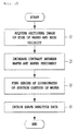
- FIG. 1 is a flowchart for describing a method of analyzing a shape of a wafer according to an embodiment of the present invention.
- FIG. 2 is a view illustrating a wafer W of which a shape is analyzed by the method illustrated in FIG. 1 and a locally enlarged cross sectional view 50 of the wafer W.
- a periphery of the wafer W is referred to as a wafer periphery (WP).
- a sectional image showing a shape of the wafer W is acquired (S10).
- the shape of the wafer W shown in the acquired sectional image of the wafer W may include shapes of an edge WE (a wafer edge) of the wafer W and an edge vicinity WF (a wafer front).
- an analysis method in which cross sectional image may be obtained such as a focused ion beam (FIB) technique may be applied.
- FIB focused ion beam
- the edge vicinity WF corresponds to a front side of the wafer W and is disposed in a vicinity of the edge WE.
- the edge WE may be divided into a bevel portion WB (a wafer bevel) and an apex WA (a wafer apex).
- the bevel portion WB refers to an inclined portion of the edge WE. That is, the bevel portion WB refers to a flat and inclined portion appearing across a point having a maximum curvature at the front side WF of the wafer W.
- the apex WA refers to an endmost portion protruding from a side of the wafer W.
- an end of the edge WE may be symmetrical based on a center of a thickness of the wafer W.
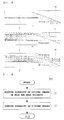
- FIGS. 3(a) to 3(c) which are views illustrating samples of three sectional images having curvatures different from one another, are views illustrating image samples in which only a portion 52 of the sectional image illustrated in FIG. 2 is enlarged.
- W represents a portion corresponding to the wafer
- WP represents a portion corresponding to the periphery of the wafer.
- a curvature of the wafer illustrated in FIG. 3(a) is the largest
- a curvature of the wafer illustrated in FIG. 3(c) is the smallest
- a curvature of the wafer illustrated in FIG. 3(b) is the middle of the curvatures of the wafers illustrated in FIG. 3(a) and FIG. 3(c) .
- a sectional image including the edge WE of the wafer W and the edge vicinity WF may be accurately captured using an electron microscope such as a scanning electron microscope (SEM) or a transmission electron microscope (TEM).
- an electron microscope such as a scanning electron microscope (SEM) or a transmission electron microscope (TEM).
- a sectional image may be obtained by capturing the wafer W one time. Or, after capturing the wafer W several times, a sectional image showing the best resolution may also be selected. For example, as illustrated in FIGS. 3(a) to 3(c) , the samples of the three sectional images may be acquired by capturing the portion 52 illustrated in FIG. 2 .
- each of a horizontal size and a vertical size of each pixel in the sectional image may be less than or equal to 1% of a size of a shape of the wafer, and preferably, may be in a range of 0.25 ⁇ m to 2 ⁇ m.
- FIG. 4 is a flowchart for describing an embodiment 10A of Operation S10 illustrated in FIG. 1 .
- FIGS. 5(a) to 5(d) are views to help understanding of divided images in example.
- a plurality of divided images of the edge WE and the edge vicinity WF are acquired (S12).
- a plurality of divided images illustrated in FIGS. 5(a) to 5(d) may be acquired by capturing the wafer W several times.
- the plurality of divided images may be acquired by the electron microscope as described above.
- the sectional image is obtained by combining the plurality of divided images (S14).
- the sectional image 50 illustrated in FIG. 2 may be acquired by combining the plurality of divided images illustrated in FIGS. 5(a) to 5(d) .
- a luminance of each of the plurality of divided images are analyzed so that intervals having a similar luminance overlap, and thus the sectional image 50 may also be acquired.
- the sectional image obtained by the combining of the plurality of divided images may have higher resolution than the sectional image captured at one time.
- the 'surface contour of the wafer W' refers to a boundary 60 between the wafer W and the wafer periphery WP.
- the boundary 60 extends over the edge vicinity WF and the edge WE.
- FIGS. 6(a) to 6(c) are views illustrating states in which contrasts of sectional image samples illustrated in FIGS. 3(a) to 3(c) are increased, respectively.
- the wafer W represented by a white color and the periphery WF of the wafer W represented by a black color may be clearly distinguished as illustrated in FIGS. 6(a) to 6(c) .
- Operation S20 may not be performed and may be omitted.
- the series of coordinates of the surface contour of the wafer W may be found using each of the sectional images illustrated in FIGS. 6(a) to 6(c) , in which the contrast is increased.
- the series of coordinates of the surface contour of the wafer W may be found using each of the sectional images illustrated in FIGS. 3(a) to 3(c) .
- FIG. 7 is a flowchart for describing an embodiment 30A of Operation S30 illustrated in FIG. 1 .
- adjacent pixels positioned at the surface contour 60 of the wafer W may have a greater luminance difference than adjacent pixels positioned in the wafer W or adjacent pixels positioned in the wafer periphery WP.
- the series of coordinates of the surface contour of the wafer W may be obtained as follows.
- a luminance of each of the pixels of the sectional image is obtained (S31).
- adjacent pixels showing a relatively large luminance difference among the luminance differences may be found, and the found adjacent pixels may be determined as the temporary contour pixels (S33).
- the threshold luminance range may be a range of a gray scale of 0.01 to a gray scale of 0.1.
- Operations S32 and S33 may be performed on all the pixels included in the sectional image, but the embodiment is not limited thereto.
- the sectional image may be grouped, a distribution of the luminance of each group in the sectional image may be obtained, and Operations S32 and S33 may be performed on only a group having a greater distribution of the luminance than that of other groups. This is because the distribution of the luminance of the pixels belonging to a group not including the surface contour of the wafer W is not large. In this case, Operations S32 and S33 may be performed within a much faster time than when Operations S32 and S33 are performed on all the pixels included in the sectional image.
- the luminance differences may be listed in order from largest to smallest, and pixels showing top level luminance differences in all the listed luminance differences may be determined as the temporary contour pixels. For example, the pixels showing top level luminance differences in a range of the top several % to several tens of % in all the listed luminance differences may be determined as the temporary contour pixels.
- the operator may examine the provided temporary surface contour with the naked eye. As a result of the examination with the naked eye, when the operator is determined that the temporary surface contour was determined incorrectly, the operator may require a modification of the temporary surface contour. For example, when the temporary surface contour is cut, is generated as a plurality of lines for example, two lines, or has a bad point, the operator may determine that the temporary surface contour is incorrect, and may require a modification of the temporary surface contour.
- FIG. 8 is an enlarged view illustrating portion 'A' illustrated in FIG. 2 .
- Operation S34 may be performed without the operator's intervention. That is, when an interval between the temporary contour pixels constituting the temporary surface contour is out of a threshold distance, it may be determined that the modification of the temporary surface contour is required. Referring to FIG. 8 , pixels P1 to P4 are assumed to be determined as the temporary contour pixels in Operation S33. In this case, intervals d1 and d2 between the temporary contour pixels P1, P2, and P3 disposed in contact with the wafer surface contour 60 are smaller than an interval d3 between the temporary contour pixel P4 disposed away from the wafer surface contour 60 and another temporary contour pixel (e.g., PI).
- PI temporary contour pixel
- the threshold distance may be determined so that modification of the temporary contour pixels P4 disposed spaced far apart from the wafer surface contour 60 may be required.
- the threshold distance may be in a range of 1 pixel to 100 pixels.
- the threshold distance may be a distance within 10% of that from the temporary surface contour 60.
- the threshold distance may be a distance corresponding to 1% of a size of the shape of the wafer W.
- the temporary contour pixels are re-determined by proceeding to Operation S33 (S33).
- an array of the temporary contour pixels determined in Operation S33 is determined as a series of coordinates of the wafer surface contour 60 (S35).
- pixels having the largest contrast between white and black in the sectional image are found as the series of coordinates of the wafer surface contour 60.
- the array of the temporary contour pixels determined as the series of coordinates of the surface contour 60 of the wafer W is converted into a series of coordinates having a form of Cartesian coordinates (S36).
- Cartesian coordinates refers to coordinates represented in a mathematical coordinate system, for example, an X-Y coordinate system, an r- ⁇ coordinate system, a ⁇ coordinate system, or the like.
- the shape of the wafer W may be quantified and may be represented numerically.
- FIGS. 9(a) to 9(c) are views illustrating the sectional images obtained by performing Operation 30 on the sectional images illustrated in FIGS. 6(a) to 6(c) , respectively.
- the array of the temporary contour pixels determined as the series of coordinates of the wafer surface contour 60 is image coordinates. That is, while the image coordinates set an upper left corner as a reference point (0, 0) in a coordinate system, the Cartesian coordinates set a lower left corner as a reference point (0, 0) in a first quadrant of a coordinate system.
- a lower left corner in a first quadrant of a series of Cartesian coordinates may be a reference point (0, 0) as illustrated in FIGS. 9(a) to 9(c) .
- Operation S30 may be performed programmatically by a program stored in a computer-readable recording medium.
- shape analysis data including information on shapes of the edge WE and the edge vicinity WF is obtained using the series of coordinates of the surface contour of the wafer W found by performing Operation S30 (S40).
- the shape analysis data may be quantified and represented.
- FIG. 10 is a flowchart for describing an embodiment 40A of Operation S40 illustrated in FIG. 1 .
- a curve made of the series of coordinates of the surface contour of the wafer W found in Operation S30 is smoothed (S42). Since the series of coordinates of the wafer surface contour found in Operation S30 is discrete, mathematically obtaining of the shape analysis data using the curve made of the series of discrete coordinates of the wafer surface contour may be difficult. Therefore, when the curve made of the series of discrete coordinates of the wafer surface contour is smoothed in order to easily and mathematically obtain and analyze the shape analysis data, the smoothed curve may be softer than the curve made of the series of discrete coordinates. Also, in this case, even when mathematical operations such as differentiations, as described below, are performed several times, the shape analysis data may be continuously and stably quantified without causing a large error.
- various known smoothing techniques such as an adjacent-averaging method, a Savitzky-Golay filter method, and the like may be used in order to perform Operation S42.
- FIGS. 11a to 11c are graphs for describing processes of smoothing of portions 72, 74, and 76 illustrated in FIG. 9(c) , respectively, where horizontal axes represent horizontal positions (x) of the wafer W and vertical axes represent vertical positions (y) of the wafer W. That is, FIG. 11a partially represents numeral 72 illustrated in FIG. 9(c) , FIG. 11b partially represents numeral 74 illustrated in FIG. 9(c) , and FIG. 11c partially represents numeral 76 illustrated in FIG. 9(c) .
- smoothed curves 92, 94, and 96 are respectively obtained by smoothing curves 82, 84, and 86 made of the series of coordinates of the surface contour of the wafer W found in Operation S30 (S42).
- shape analysis data is calculated using the smoothed curves 92, 94, and 96, and the calculated shape analysis data is provided in various forms (S44).
- the shape analysis data may be quantified.
- the shape analysis data may include a curvature formed by both of the edge WE and the edge vicinity WF. That is, the smoothed curves 92, 94, and 96 may be converted into quantified data (or, numerical data) such as a curvature.
- x and y represent a horizontal position and a vertical position of a wafer W, respectively.
- first and second differentiations should be performed.
- the series of coordinates of the surface contour of the wafer W since the series of coordinates of the surface contour of the wafer W is found based on pixels, the series of coordinates of the surface contour of the wafer W has a discrete characteristic as described above. Therefore, when the curve made of the series of discrete coordinates is not smoothed and first and the second differentiations are performed on the curve, a large error may occur. Therefore, when the curves 82, 84, and 86 made of the series of coordinates of the wafer surface contour are smoothed as in Operation S42, such an error may be prevented from occurring while maintaining the information on the shape of the wafer edge.
- FIG. 12 is a graph illustrating results a, b, and c that the first differentiation is performed on results that the curves made of the series of discrete coordinates in the sectional images illustrated in FIGS. 9(a) to 9(c) , are smoothed, respectively, where a horizontal axis represents a horizontal position x of the wafer W, and a vertical axis represents a first differentiation value.
- FIG. 13 is a graph illustrating curvatures a, b, and c obtained by substituting results that the curves made of the series of discrete coordinates in the sectional images illustrated in FIGS. 9(a) to 9(c) are smoothed, respectively, into Equation 1, where a horizontal axis represents a horizontal position x of the wafer W, and a vertical axis represents a curvature C.
- Equation 1 curvatures with respect to the three sectional image samples may be quantified as illustrated in FIG. 13 .
- the curvature a formed by the wafer surface contour 60 at the edge WE and the edge vicinity WF in the sample illustrated in FIG. 3(a) is largest, and the curvature c formed by the wafer surface contour 60 at the edge WE and the edge vicinity WF in the sample illustrated in FIG. 3(c) is smallest. Therefore, since the wafer surface contour 60 is most smoothly changed from the edge WE to the edge vicinity WF when comparing the sample illustrated in FIG. 3(c) having the smallest curvature with the other two samples, it may be seen that the sample illustrated in FIG. 3(c) has a good edge shape.
- the shape analysis data may include a 'normalized gap area (NGA).
- NGA 'normalized gap area
- the shape analysis data includes the curvatures for relatively comparing different samples.
- the NGA may be an absolute indicator for analyzing the shape of the edge.
- GA represents a gap area
- UPA represents an unprocessed area
- PA represents a processed area.
- 'an edge vicinity tangent' and 'a bevel tangent' are defined as follows.
- the edge vicinity tangent which is a tangent at a first point P1 of the wafer surface contour 60 positioned in the edge vicinity WF, refers to an extension line of an upper horizontal plane of the wafer W.
- the bevel tangent refers to a tangent at a second point P2 that is a basis for a taper angle ⁇ t of the bevel portion WB in the wafer surface contour 60 positioned in the bevel portion WB.
- the edge vicinity tangent and the bevel tangent are disposed based on a point having a maximum curvature in the wafer surface contour 60.
- the UPA refers to an area having a trapezoidal shape, which is made of a reference point on a mathematical coordinate system, for example, an X-Y coordinate system, the first point P1, the second point P2, and an intersection of the edge vicinity tangent and the bevel tangent.
- a mathematical coordinate system for example, an X-Y coordinate system
- the UPA is defined as having the trapezoidal shape rather than a rectangular shape. That is, the trapezoidal shape actually surrounds the wafer surface contour 60.
- the PA refers to an area made of the reference point on the mathematical coordinate system, for example, the X-Y coordinate system, the first point P1, the second point P2, and the wafer edge contour 60 of the edge vicinity WF and the bevel portion WB.
- the GA since an absolute value of the GA may be affected by a size or a degree of twist of the image captured for the measurement, the GA is normalized into the UPA and the NGA may be used as the shape analysis data.
- the reference point on the X-Y coordinate system used in defining the above-described UPA and the above-described PA may be, for example, an x value (referred to as 'x1') of the first point P1 and a y value (referred to as 'y1') of the second point P2.
- the above-described NGA will be described as follows with reference to the accompanying drawings.
- the NGA will be described by assuming that the wafer surface contour 60 used in defining the edge vicinity tangent and the bevel tangent refers to the wafer surface contour 60 which is smoothed in Operation S42.
- FIG. 14 is a view illustrating an example of a smoothed curve for describing an NGA, where a horizontal axis represents a horizontal position x of the wafer W, and a vertical axis represents a vertical position y of the wafer W.
- an edge vicinity tangent CL1 which is a tangent at the first point P1 of the wafer surface contour 60 positioned in the edge vicinity WF, may correspond to an extension line of an upper horizontal plane of the wafer W.
- a bevel tangent CL2 is positioned on the wafer surface contour 60 positioned in the bevel portion WB, and refers to a tangent at the second point P2 that is a basis for a taper angle ⁇ t of the bevel portion WB.
- the UPA refers to an area having a trapezoidal shape made of a reference point (x1, y1), the first point P1, the second point P2, and an intersection P3 of the tangents CL1 and CL2, in FIG. 14 .
- the PA refers to an area made of the reference point (x1, y1), the first point P1, the second point P2, and the wafer surface contour 60.
- the reference point (x1, y1) may be a point (-100, 20.5) as illustrated in FIG. 14 , or may be a lower left corner (0, 0) in the first quadrant of the coordinate system illustrated in FIGS. 9(a) to 9(c) .
- a shaded GA in FIG. 14 may be obtained, and the NGA may be obtained by normalizing the GA to be the UPA.
- the shape analysis data such as the above-described NGA may be used to analyze the shape of the wafer W, particularly, the edge of the wafer W, through a relationship with the other shape analysis data.
- the slope angle ⁇ s refers to an angle between the edge vicinity tangent CL1 and the wafer surface contour 60 of the edge vicinity WF.
- points which are referred to below and illustrated in each of graphs of FIGS. 15 to 18 are values measured at portions that are not contaminated by particles and the like.
- FIG. 15 is a graph illustrating a relationship between an NGA and a maximum curvature of an edge, where a horizontal axis represents the maximum curvature of the edge, and a vertical axis represents the NGA.
- the NGA is decreased. This is because, referring to FIG. 14 , as the maximum curvature is increased, the surface contour 60 of the wafer W is moved toward a positive direction of a y-axis as illustrated by arrow 62 of FIG. 14 .
- FIG. 16 is a graph illustrating a relationship between an NGA and a curvature radius of an edge, where a horizontal axis represents the curvature radius of the edge, and a vertical axis represents the NGA.
- the curvature radius has an inverse relationship with respect to the curvature, as the curvature radius is increased, it may be seen that the NGA is increased.
- FIG. 17 is a graph illustrating a relationship between an NGA and a slope angle ⁇ s, where a horizontal axis represents the slope angle ⁇ s, and a vertical axis represents the NGA.
- FIG. 18 is a graph illustrating a relationship between an NGA and a taper angle ⁇ t, where a horizontal axis represents the taper angle ⁇ t, and a vertical axis represents the NGA.
- the NGA shows consistency in all various types of shape analysis data such as the maximum curvature, the curvature radius, the slope angle ⁇ s, and the taper angle ⁇ t. In this way, in analyzing the edge shape of the wafer, it may be seen that the NGA is usefully used.
- the sectional shape having high resolution with respect to the edge WE of the wafer W and the edge vicinity WF is acquired, and coordinates of a wafer surface contour in the acquired sectional image may be represented as a curve in a mathematical coordinate system from an image coordinate system. Therefore, as the curve is mathematically processed, the curvature which is one type of the shape analysis data of the edge is quantified as illustrated in FIG. 13 and may be relatively compared, and the NGA which is another type of the shape analysis data of the edge is compared with the other types of the shape analysis data as illustrated in FIGS. 15 to 18 , and thus the shape of the edge may be analyzed. In addition, roughness, a gradient, an inclined angle, and the like of the wafer surface may be easily mathematically analyzed using a smoothed curve.
- a wafer shape analyzing apparatus according to the embodiment in which the above-described method of analyzing the shape of the wafer illustrated in FIG. 1 , for example, the method of analyzing the edge shape of the wafer, is performed will be described as follows with reference to the accompanying drawings.
- the method of analyzing the shape of the wafer illustrated in FIG. 1 may also be performed in a wafer shape analyzing apparatus having a configuration different from that of the apparatus described as follows.
- operations of each unit of a wafer shape analyzing apparatus to be described below will be described briefly with reference to FIGS. 1 , 4 , 7 , and 10 described above.
- FIG. 19 is a block diagram of a wafer shape analyzing apparatus 200 according to an embodiment, which includes an image acquisition unit 210, a contrast adjusting unit 220, a surface contour determining unit 230, and a data analyzing unit 240.
- the image acquisition unit 210 acquires a sectional image showing a shape of a wafer W to be analyzed, and outputs the acquired sectional image to the contrast adjusting unit 220.
- the shape of the wafer shown in the obtained sectional image may include an edge WE and an edge vicinity WF.
- FIG. 20 is a block diagram of an embodiment 210A of the image acquisition unit 210 illustrated in FIG. 19 which includes an image capturing unit 212 and an image combining unit 214.
- the image capturing unit 212 acquires a plurality of divided images by capturing the edge WE of the wafer W and the edge vicinity WF several times, and outputs the obtained divided images to the image combining unit 214. That is, since the image capturing unit 212 performs Operation S12 illustrated in FIG. 4 , description identical to that of Operation S12 described above will be omitted.
- the image combining unit 214 generates a sectional image by combining the plurality of divided images received from the image capturing unit 212, and outputs the generated sectional image to the contrast adjusting unit 220 through an output terminal OUT3. Since the image combining unit 214 performs Operation S14 illustrated in FIG. 4 , description identical to that of Operation S14 described above will be omitted.
- the contrast adjusting unit 220 increases a contrast between the wafer W and a wafer periphery WP in the sectional image received from the image acquisition unit 210, and outputs the sectional image in which the contrast is increased to the surface contour determining unit 230. Since the contrast adjusting unit 220 performs Operation S20 illustrated in FIG. 1 , description identical to that of Operation S20 described above will be omitted.
- the surface contour determining unit 230 finds a series of coordinates of a wafer surface contour in the sectional image which is output from the contrast adjusting unit 220 and in which the contrast is increased, and outputs the series of found coordinates to the data analyzing unit 240.
- the surface contour determining unit 230 finds the series of coordinates of the surface contour of the wafer W in the sectional image output from the image acquisition unit 210, and outputs the found result to the data analyzing unit 240.
- the surface contour determining unit 230 serves to perform Operation S30 illustrated in FIG. 1 .
- the wafer shape analyzing apparatus 200 illustrated in FIG. 19 is described to include the contrast adjusting unit 220 for convenience of description, the embodiment is not limited thereto.
- FIG. 21 is a block diagram of an embodiment 230A of the surface contour determining unit 230 illustrated in FIG. 19 which includes a luminance determining unit 232, a luminance difference calculating unit 234, a temporary contour pixel determining unit 235, a contour modification checking unit 236, a coordinate series determining unit 237, and a coordinate conversion unit 238.
- the luminance determining unit 232 determines a luminance of each pixel in the sectional image received from the contrast adjusting unit 220 through an input terminal IN2, and outputs the determined luminance to the luminance difference calculating unit 234. Since the luminance determining unit 232 performs Operation S31 illustrated in FIG. 7 , description identical to that of Operation S31 described above will be omitted.
- the luminance difference calculating unit 234 receives the luminance output from the luminance determining unit 232, calculates luminance differences between adjacent pixels, and outputs the calculated luminance difference to the temporary contour pixel determining unit 235. Since the luminance difference calculating unit 234 performs Operation S32 illustrated in FIG. 7 , description identical to that of Operation S32 described above will be omitted.
- the temporary contour pixel determining unit 235 determines temporary contour pixels using the luminance differences received from the luminance difference calculating unit 234, and outputs the determined temporary contour pixels to the contour modification checking unit 236.
- the temporary contour pixel determining unit 235 may find adjacent pixels showing a relatively large luminance difference among the luminance differences calculated in the luminance difference calculating unit 234, determine the found adjacent pixels as the temporary contour pixels, and output the determined temporary contour pixels to the contour modification checking unit 236.
- the temporary contour pixel determining unit 235 may list the luminance differences calculated in the luminance difference calculating unit 234 in order from largest to smallest, determine pixels showing top level luminance differences in all the listed luminance differences as the temporary contour pixels, and output the determined temporary contour pixels to the contour modification checking unit 236.
- the temporary contour pixel determining unit 235 may provide a temporary surface contour made of the determined temporary contour pixels to the operator through an output terminal OUT2.
- the temporary contour pixel determining unit 235 modifies (or re-determines) the temporary contour pixels, or outputs an array of the temporary contour pixels which are initially determined or re-determined to the coordinate series determining unit 237 in response to a modification request signal output from the contour modification checking unit 236.
- the coordinate series determining unit 237 determines the array of the temporary contour pixels received from the temporary contour pixel determining unit 235 as a series of coordinates of a surface contour of the wafer, and outputs the series of determined coordinates to the coordinate conversion unit 238. That is, since the coordinate series determining unit 237 performs Operation S35 illustrated in FIG. 7 , description identical to that of Operation S35 described above will be omitted.
- the contour modification checking unit 236 checks whether modification of the temporary surface contour formed by the temporary contour pixels is required, generates a modification request signal according to the checked result, and outputs the modification request signal to the temporary contour pixel determining unit 235.
- the operator may examine the temporary surface contour provided from the temporary contour pixel determining unit 235 through the output terminal OUT2 with the naked eye.
- the operator may require the modification of the temporary surface contour through an input terminal IN1 to the temporary contour pixel determining unit 235 via the contour modification checking unit 236.
- the contour modification checking unit 236 determines whether the modification of the temporary surface contour is required by the operator through the input terminal IN1, and generates a modification request signal and outputs the generated modification request signal to the temporary contour pixel determining unit 235 when it is determined that the modification of the temporary surface contour is required.
- the contour modification checking unit 236 may determine whether an interval between the temporary contour pixels output from the temporary contour pixel determining unit 235 is out of a threshold distance, and generate a modification request signal and output the generated modification request signal to the temporary contour pixel determining unit 235 when it is determined that the modification of the temporary surface contour is required according to the determined result.
- contour modification checking unit 236 performs Operation S34 illustrated in FIG. 7 , description identical to that of Operation S34 described above will be omitted.
- the coordinate conversion unit 238 receives the array of the temporary contour pixels determined as the series of coordinates of the surface contour from the coordinate series determining unit 237, converts the array of the temporary contour pixels into a series of coordinates having a form of Cartesian coordinates, and outputs the series of converted coordinates of the surface contour having the form of Cartesian coordinates to the data analyzing unit 240 through an output terminal OUT4. Since the coordinate conversion unit 238 performs Operation S36 illustrated in FIG. 7 , description identical to that of Operation S36 described above will be omitted.
- the data analyzing unit 240 calculates shape analysis data including information on the shape of the edge and the edge vicinity using the series of coordinates of the wafer surface contour output from the surface contour determining unit 230, and outputs the calculated shape analysis data through an output terminal OUT1.
- the data analyzing unit 240 performs Operation S40 illustrated in FIG. 1 .
- FIG. 22 is a block diagram illustrating an embodiment 240A of the data analyzing unit 240 illustrated in FIG. 19 which includes a smoothing unit 242, a data calculating unit 244, and a data output unit 246.
- the smoothing unit 242 smooths a curve made of a series of discrete coordinates of the surface contour, and outputs the smoothed result to the data calculating unit 244. Since the smoothing unit 242 performs Operation S42 illustrated in FIG. 10 , description identical to that of Operation S42 described above will be omitted.
- the data calculating unit 244 quantifies and calculates the shape analysis data using the smoothed curve output from the smoothing unit 242, and outputs the calculated result to the data output unit 246.
- the data output unit 246 outputs the calculated result received from the data calculating unit 244 as various types of the shape analysis data through the output terminal OUT1.
- the data output unit 246 may output the shape analysis data in a numerical form such as a curvature or angles ⁇ s and ⁇ t, or may output the shape analysis data in a visual form such as a graph of differentiation values, curvatures, or the like with respect to the shape of the wafer.
- the embodiments may be used to manufacture and analyze a wafer.
Landscapes
- Engineering & Computer Science (AREA)
- Physics & Mathematics (AREA)
- Computer Vision & Pattern Recognition (AREA)
- General Physics & Mathematics (AREA)
- Theoretical Computer Science (AREA)
- Quality & Reliability (AREA)
- Geometry (AREA)
- Testing Or Measuring Of Semiconductors Or The Like (AREA)
- Image Analysis (AREA)
- Length Measuring Devices By Optical Means (AREA)
- Image Processing (AREA)
Applications Claiming Priority (2)
| Application Number | Priority Date | Filing Date | Title |
|---|---|---|---|
| KR1020130162085A KR101540569B1 (ko) | 2013-12-24 | 2013-12-24 | 웨이퍼의 형상 분석 방법 및 장치 |
| PCT/KR2014/005620 WO2015099251A1 (ko) | 2013-12-24 | 2014-06-25 | 웨이퍼의 형상 분석 방법 및 장치 |
Publications (3)
| Publication Number | Publication Date |
|---|---|
| EP3089202A1 true EP3089202A1 (de) | 2016-11-02 |
| EP3089202A4 EP3089202A4 (de) | 2017-06-14 |
| EP3089202B1 EP3089202B1 (de) | 2020-10-21 |
Family
ID=53479080
Family Applications (1)
| Application Number | Title | Priority Date | Filing Date |
|---|---|---|---|
| EP14875737.0A Active EP3089202B1 (de) | 2013-12-24 | 2014-06-25 | Verfahren und vorrichtung form zur analyse der form eines wafers |
Country Status (6)
| Country | Link |
|---|---|
| US (1) | US9904994B2 (de) |
| EP (1) | EP3089202B1 (de) |
| JP (1) | JP6240782B2 (de) |
| KR (1) | KR101540569B1 (de) |
| CN (1) | CN105849886B (de) |
| WO (1) | WO2015099251A1 (de) |
Cited By (2)
| Publication number | Priority date | Publication date | Assignee | Title |
|---|---|---|---|---|
| EP3671816A4 (de) * | 2017-08-15 | 2021-04-28 | Shin-Etsu Handotai Co., Ltd. | Beurteilungsverfahren und beurteilungsvorrichtung der kantenform eines siliciumwafers, siliciumwafer und auswahlverfahren und herstellungsverfahren dafür |
| WO2022225545A1 (en) | 2021-04-19 | 2022-10-27 | Kla Corporation | Edge profile inspection for delamination defects |
Families Citing this family (18)
| Publication number | Priority date | Publication date | Assignee | Title |
|---|---|---|---|---|
| KR101540569B1 (ko) * | 2013-12-24 | 2015-07-31 | 주식회사 엘지실트론 | 웨이퍼의 형상 분석 방법 및 장치 |
| US11557048B2 (en) | 2015-11-16 | 2023-01-17 | Applied Materials, Inc. | Thickness measurement of substrate using color metrology |
| US10565701B2 (en) | 2015-11-16 | 2020-02-18 | Applied Materials, Inc. | Color imaging for CMP monitoring |
| JP6821263B2 (ja) * | 2017-05-26 | 2021-01-27 | 株式会社ディスコ | チップの曲率を測定する方法及び測定する装置 |
| JP6841202B2 (ja) | 2017-10-11 | 2021-03-10 | 株式会社Sumco | 半導体ウェーハの評価方法および半導体ウェーハの製造方法 |
| KR101992778B1 (ko) * | 2017-11-01 | 2019-06-25 | 에스케이실트론 주식회사 | 웨이퍼 및 그 형상 분석 방법 |
| CN108828267B (zh) * | 2018-03-19 | 2021-05-25 | 长江存储科技有限责任公司 | 晶圆翘曲程度测量方法及装置 |
| WO2019198458A1 (ja) * | 2018-04-13 | 2019-10-17 | 株式会社Sumco | 半導体ウェーハの評価方法および半導体ウェーハの製造方法 |
| KR20190134158A (ko) | 2018-05-25 | 2019-12-04 | 이중희 | 차 추출장치 및 추출방법 |
| KR102119662B1 (ko) * | 2018-09-18 | 2020-06-05 | 인하대학교 산학협력단 | 아노다이징된 금속 표면 구조의 일관성 정량화 방법 |
| US20200147691A1 (en) * | 2018-11-14 | 2020-05-14 | Applied Materieals, Inc. | Ultrasonic Monitoring of Additive Manufacturing |
| US11100628B2 (en) * | 2019-02-07 | 2021-08-24 | Applied Materials, Inc. | Thickness measurement of substrate using color metrology |
| KR102457699B1 (ko) * | 2020-07-16 | 2022-10-24 | 에스케이실트론 주식회사 | 웨이퍼 및 그 형상 분석 방법 |
| JP6915181B1 (ja) * | 2021-02-02 | 2021-08-04 | オリエンタル白石株式会社 | 刃口境界部判定システム及びプログラム |
| CN113421297B (zh) * | 2021-07-02 | 2023-06-27 | 浙江德菲洛智能机械制造有限公司 | 一种草莓的形状对称性分析方法 |
| CN114361074B (zh) * | 2021-12-31 | 2025-03-18 | 匠岭科技(上海)有限公司 | 晶圆解键合方法 |
| KR102911216B1 (ko) * | 2023-04-26 | 2026-01-13 | 에스케이실트론 주식회사 | 웨이퍼의 형상 분석 방법 |
| CN121013965A (zh) * | 2023-04-26 | 2025-11-25 | 爱思开矽得荣株式会社 | 晶圆及其形状分析方法 |
Family Cites Families (24)
| Publication number | Priority date | Publication date | Assignee | Title |
|---|---|---|---|---|
| JP3543442B2 (ja) * | 1995-09-26 | 2004-07-14 | 松下電工株式会社 | 物品の干渉検出方法 |
| US6064388A (en) * | 1997-11-10 | 2000-05-16 | Cognex Corporation | Cartesian to polar coordinate transformation |
| KR100361962B1 (ko) * | 2000-02-03 | 2002-11-23 | (주) 셀라이트 | 웨이퍼 테두리 결함 검사장치 및 검사방법 |
| JP4076343B2 (ja) * | 2001-12-05 | 2008-04-16 | 株式会社小松製作所 | 半導体ウェハのドットマーク形成位置の位置決め方法とその位置決め装置 |
| JP3656910B2 (ja) * | 2002-07-22 | 2005-06-08 | 住友電気工業株式会社 | スクライブ溝の加工方法及びスクライブ装置 |
| JP4338405B2 (ja) | 2003-01-15 | 2009-10-07 | パナソニック株式会社 | サイズ測定システムおよびサイズ測定装置 |
| US7138629B2 (en) * | 2003-04-22 | 2006-11-21 | Ebara Corporation | Testing apparatus using charged particles and device manufacturing method using the testing apparatus |
| JP4331541B2 (ja) * | 2003-08-06 | 2009-09-16 | オリンパス株式会社 | 内視鏡装置 |
| WO2006025386A1 (ja) * | 2004-08-31 | 2006-03-09 | Nikon Corporation | 位置合わせ方法、処理システム、基板の投入再現性計測方法、位置計測方法、露光方法、基板処理装置、計測方法及び計測装置 |
| KR20060088817A (ko) * | 2005-01-28 | 2006-08-07 | 가부시키가이샤 이빔 | 기판처리장치 및 기판처리방법 |
| EP1872392B1 (de) | 2005-04-19 | 2012-02-22 | Ebara Corporation | Substratverarbeitungsvorrichtung |
| JP4787012B2 (ja) * | 2005-12-13 | 2011-10-05 | 大倉インダストリー株式会社 | 断面形状測定装置及び断面形状測定方法 |
| JP4827127B2 (ja) * | 2006-03-24 | 2011-11-30 | 株式会社トプコン | 検査装置 |
| JP4065893B1 (ja) * | 2006-12-04 | 2008-03-26 | 東京エレクトロン株式会社 | 欠陥検出装置、欠陥検出方法、情報処理装置、情報処理方法及びそのプログラム |
| JP2008205042A (ja) * | 2007-02-16 | 2008-09-04 | Renesas Technology Corp | 半導体集積回路装置の製造方法 |
| KR101099264B1 (ko) * | 2007-03-30 | 2011-12-26 | 시바우라 메카트로닉스 가부시키가이샤 | 반도체 웨이퍼의 가장자리 검사 장치 및 가장자리 검사 방법 |
| KR100952316B1 (ko) | 2008-03-21 | 2010-04-12 | 금호타이어 주식회사 | 타이어의 숄더 스트립 자동 부착 장치 |
| JP5469839B2 (ja) * | 2008-09-30 | 2014-04-16 | 株式会社日立ハイテクノロジーズ | 物体表面の欠陥検査装置および方法 |
| JP4734398B2 (ja) | 2008-12-04 | 2011-07-27 | 株式会社コベルコ科研 | 形状測定装置,形状測定方法 |
| DE102009012997A1 (de) * | 2009-03-13 | 2010-09-16 | Bst International Gmbh | Verfahren und Vorrichtung zum Messen der Lage der Kante einer Materialbahn |
| JP2011085410A (ja) * | 2009-10-13 | 2011-04-28 | Nippon Steel Corp | エッジ検出装置、エッジ検出方法、およびプログラム |
| CN102985386B (zh) * | 2010-07-08 | 2015-09-02 | 旭硝子株式会社 | 玻璃基板端面的评价方法及玻璃基板端面的加工方法以及玻璃基板 |
| JP5417358B2 (ja) * | 2011-02-28 | 2014-02-12 | 株式会社日立ハイテクノロジーズ | 画像処理装置、及び画像処理を行うためのコンピュータープログラム |
| KR101540569B1 (ko) * | 2013-12-24 | 2015-07-31 | 주식회사 엘지실트론 | 웨이퍼의 형상 분석 방법 및 장치 |
-
2013
- 2013-12-24 KR KR1020130162085A patent/KR101540569B1/ko active Active
-
2014
- 2014-06-25 EP EP14875737.0A patent/EP3089202B1/de active Active
- 2014-06-25 WO PCT/KR2014/005620 patent/WO2015099251A1/ko not_active Ceased
- 2014-06-25 JP JP2016540002A patent/JP6240782B2/ja active Active
- 2014-06-25 CN CN201480070870.4A patent/CN105849886B/zh active Active
- 2014-06-25 US US15/105,240 patent/US9904994B2/en active Active
Cited By (5)
| Publication number | Priority date | Publication date | Assignee | Title |
|---|---|---|---|---|
| EP3671816A4 (de) * | 2017-08-15 | 2021-04-28 | Shin-Etsu Handotai Co., Ltd. | Beurteilungsverfahren und beurteilungsvorrichtung der kantenform eines siliciumwafers, siliciumwafer und auswahlverfahren und herstellungsverfahren dafür |
| US11486833B2 (en) | 2017-08-15 | 2022-11-01 | Shin-Etsu Handotai Co., Ltd. | Method for evaluating edge shape of silicon wafer, apparatus for evaluating thereof, silicon wafer, method for selecting and method for manufacturing thereof |
| TWI784034B (zh) * | 2017-08-15 | 2022-11-21 | 日商信越半導體股份有限公司 | 矽晶圓的邊緣形狀的評價方法及評價裝置、矽晶圓及篩選方法以及其製造方法 |
| EP3671816B1 (de) * | 2017-08-15 | 2025-10-15 | Shin-Etsu Handotai Co., Ltd. | Beurteilungsverfahren und beurteilungsvorrichtung der kantenform eines siliciumwafers, siliciumwafer und auswahlverfahren und herstellungsverfahren dafür |
| WO2022225545A1 (en) | 2021-04-19 | 2022-10-27 | Kla Corporation | Edge profile inspection for delamination defects |
Also Published As
| Publication number | Publication date |
|---|---|
| EP3089202B1 (de) | 2020-10-21 |
| CN105849886B (zh) | 2019-08-16 |
| JP6240782B2 (ja) | 2017-11-29 |
| US20160314577A1 (en) | 2016-10-27 |
| KR20150074370A (ko) | 2015-07-02 |
| JP2017503164A (ja) | 2017-01-26 |
| WO2015099251A1 (ko) | 2015-07-02 |
| CN105849886A (zh) | 2016-08-10 |
| KR101540569B1 (ko) | 2015-07-31 |
| EP3089202A4 (de) | 2017-06-14 |
| US9904994B2 (en) | 2018-02-27 |
Similar Documents
| Publication | Publication Date | Title |
|---|---|---|
| EP3089202B1 (de) | Verfahren und vorrichtung form zur analyse der form eines wafers | |
| TWI731559B (zh) | 電子束觀察裝置,電子束觀察系統,電子束觀察裝置中的圖像修正方法及用於圖像修正的修正係數算出方法 | |
| JP2009085657A (ja) | 走査型電子顕微鏡を用いた試料の観察方法およびそのシステム | |
| JP5500871B2 (ja) | テンプレートマッチング用テンプレート作成方法、及びテンプレート作成装置 | |
| JP6591348B2 (ja) | 検査方法 | |
| US7439503B2 (en) | Charged particle beam irradiation method, method of manufacturing semiconductor device and charged particle beam apparatus | |
| JP5651428B2 (ja) | パターン測定方法,パターン測定装置及びそれを用いたプログラム | |
| JP4974737B2 (ja) | 荷電粒子システム | |
| JP6250294B2 (ja) | 集束イオンビーム装置、それを用いた試料の断面観察方法、及び集束イオンビームを用いた試料の断面観察用コンピュータプログラム | |
| JP2013186100A (ja) | 形状検査方法およびその装置 | |
| US20090212215A1 (en) | Scanning electron microscope and method of measuring pattern dimension using the same | |
| US9978558B2 (en) | Scanning-electron-microscope image processing device and scanning method | |
| KR102803578B1 (ko) | 프로세서 시스템, 반도체 검사 시스템 및 프로그램 | |
| KR102853085B1 (ko) | 기판 불량 검출 방법 및 장치 | |
| JP2007047930A (ja) | 画像処理装置及び検査装置 | |
| KR20220062635A (ko) | 검사 시스템, 및 비일시적 컴퓨터 판독 가능 매체 | |
| JP6850234B2 (ja) | 荷電粒子線装置 | |
| JP2535695B2 (ja) | 走査型電子顕微鏡の自動焦点合わせ方法 | |
| Miao et al. | Picometer-precision atomic position tracking through electron microscopy | |
| CN103201819B (zh) | 图案判定装置以及凹凸判定方法 | |
| JP2008116206A (ja) | パターン寸法測定装置、方法及びプログラム | |
| WO2026018408A1 (ja) | 画像処理システム、画像処理方法、および表示装置 | |
| CN116989667A (zh) | 基于霍夫变换图像分析的显微镜载物台位移误差校准方法 | |
| WO2021149117A1 (ja) | 荷電粒子線画像用解析装置、検査システムおよびプログラム |
Legal Events
| Date | Code | Title | Description |
|---|---|---|---|
| PUAI | Public reference made under article 153(3) epc to a published international application that has entered the european phase |
Free format text: ORIGINAL CODE: 0009012 |
|
| 17P | Request for examination filed |
Effective date: 20160622 |
|
| AK | Designated contracting states |
Kind code of ref document: A1 Designated state(s): AL AT BE BG CH CY CZ DE DK EE ES FI FR GB GR HR HU IE IS IT LI LT LU LV MC MK MT NL NO PL PT RO RS SE SI SK SM TR |
|
| AX | Request for extension of the european patent |
Extension state: BA ME |
|
| DAX | Request for extension of the european patent (deleted) | ||
| A4 | Supplementary search report drawn up and despatched |
Effective date: 20170516 |
|
| RIC1 | Information provided on ipc code assigned before grant |
Ipc: G06T 7/60 20170101ALI20170510BHEP Ipc: H01L 21/66 20060101AFI20170510BHEP Ipc: G06T 7/00 20170101ALI20170510BHEP Ipc: H01L 21/20 20060101ALI20170510BHEP |
|
| STAA | Information on the status of an ep patent application or granted ep patent |
Free format text: STATUS: EXAMINATION IS IN PROGRESS |
|
| 17Q | First examination report despatched |
Effective date: 20190701 |
|
| RAP1 | Party data changed (applicant data changed or rights of an application transferred) |
Owner name: SK SILTRON CO., LTD. |
|
| GRAP | Despatch of communication of intention to grant a patent |
Free format text: ORIGINAL CODE: EPIDOSNIGR1 |
|
| STAA | Information on the status of an ep patent application or granted ep patent |
Free format text: STATUS: GRANT OF PATENT IS INTENDED |
|
| INTG | Intention to grant announced |
Effective date: 20200511 |
|
| GRAS | Grant fee paid |
Free format text: ORIGINAL CODE: EPIDOSNIGR3 |
|
| GRAA | (expected) grant |
Free format text: ORIGINAL CODE: 0009210 |
|
| STAA | Information on the status of an ep patent application or granted ep patent |
Free format text: STATUS: THE PATENT HAS BEEN GRANTED |
|
| AK | Designated contracting states |
Kind code of ref document: B1 Designated state(s): AL AT BE BG CH CY CZ DE DK EE ES FI FR GB GR HR HU IE IS IT LI LT LU LV MC MK MT NL NO PL PT RO RS SE SI SK SM TR |
|
| REG | Reference to a national code |
Ref country code: GB Ref legal event code: FG4D |
|
| REG | Reference to a national code |
Ref country code: CH Ref legal event code: EP |
|
| REG | Reference to a national code |
Ref country code: IE Ref legal event code: FG4D |
|
| REG | Reference to a national code |
Ref country code: DE Ref legal event code: R096 Ref document number: 602014071561 Country of ref document: DE |
|
| REG | Reference to a national code |
Ref country code: AT Ref legal event code: REF Ref document number: 1326718 Country of ref document: AT Kind code of ref document: T Effective date: 20201115 |
|
| REG | Reference to a national code |
Ref country code: AT Ref legal event code: MK05 Ref document number: 1326718 Country of ref document: AT Kind code of ref document: T Effective date: 20201021 |
|
| REG | Reference to a national code |
Ref country code: NL Ref legal event code: MP Effective date: 20201021 |
|
| PG25 | Lapsed in a contracting state [announced via postgrant information from national office to epo] |
Ref country code: GR Free format text: LAPSE BECAUSE OF FAILURE TO SUBMIT A TRANSLATION OF THE DESCRIPTION OR TO PAY THE FEE WITHIN THE PRESCRIBED TIME-LIMIT Effective date: 20210122 Ref country code: PT Free format text: LAPSE BECAUSE OF FAILURE TO SUBMIT A TRANSLATION OF THE DESCRIPTION OR TO PAY THE FEE WITHIN THE PRESCRIBED TIME-LIMIT Effective date: 20210222 Ref country code: NO Free format text: LAPSE BECAUSE OF FAILURE TO SUBMIT A TRANSLATION OF THE DESCRIPTION OR TO PAY THE FEE WITHIN THE PRESCRIBED TIME-LIMIT Effective date: 20210121 Ref country code: NL Free format text: LAPSE BECAUSE OF FAILURE TO SUBMIT A TRANSLATION OF THE DESCRIPTION OR TO PAY THE FEE WITHIN THE PRESCRIBED TIME-LIMIT Effective date: 20201021 Ref country code: RS Free format text: LAPSE BECAUSE OF FAILURE TO SUBMIT A TRANSLATION OF THE DESCRIPTION OR TO PAY THE FEE WITHIN THE PRESCRIBED TIME-LIMIT Effective date: 20201021 Ref country code: FI Free format text: LAPSE BECAUSE OF FAILURE TO SUBMIT A TRANSLATION OF THE DESCRIPTION OR TO PAY THE FEE WITHIN THE PRESCRIBED TIME-LIMIT Effective date: 20201021 |
|
| REG | Reference to a national code |
Ref country code: LT Ref legal event code: MG4D |
|
| PG25 | Lapsed in a contracting state [announced via postgrant information from national office to epo] |
Ref country code: IS Free format text: LAPSE BECAUSE OF FAILURE TO SUBMIT A TRANSLATION OF THE DESCRIPTION OR TO PAY THE FEE WITHIN THE PRESCRIBED TIME-LIMIT Effective date: 20210221 Ref country code: PL Free format text: LAPSE BECAUSE OF FAILURE TO SUBMIT A TRANSLATION OF THE DESCRIPTION OR TO PAY THE FEE WITHIN THE PRESCRIBED TIME-LIMIT Effective date: 20201021 Ref country code: LV Free format text: LAPSE BECAUSE OF FAILURE TO SUBMIT A TRANSLATION OF THE DESCRIPTION OR TO PAY THE FEE WITHIN THE PRESCRIBED TIME-LIMIT Effective date: 20201021 Ref country code: SE Free format text: LAPSE BECAUSE OF FAILURE TO SUBMIT A TRANSLATION OF THE DESCRIPTION OR TO PAY THE FEE WITHIN THE PRESCRIBED TIME-LIMIT Effective date: 20201021 Ref country code: BG Free format text: LAPSE BECAUSE OF FAILURE TO SUBMIT A TRANSLATION OF THE DESCRIPTION OR TO PAY THE FEE WITHIN THE PRESCRIBED TIME-LIMIT Effective date: 20210121 Ref country code: AT Free format text: LAPSE BECAUSE OF FAILURE TO SUBMIT A TRANSLATION OF THE DESCRIPTION OR TO PAY THE FEE WITHIN THE PRESCRIBED TIME-LIMIT Effective date: 20201021 Ref country code: ES Free format text: LAPSE BECAUSE OF FAILURE TO SUBMIT A TRANSLATION OF THE DESCRIPTION OR TO PAY THE FEE WITHIN THE PRESCRIBED TIME-LIMIT Effective date: 20201021 |
|
| PG25 | Lapsed in a contracting state [announced via postgrant information from national office to epo] |
Ref country code: HR Free format text: LAPSE BECAUSE OF FAILURE TO SUBMIT A TRANSLATION OF THE DESCRIPTION OR TO PAY THE FEE WITHIN THE PRESCRIBED TIME-LIMIT Effective date: 20201021 |
|
| REG | Reference to a national code |
Ref country code: DE Ref legal event code: R097 Ref document number: 602014071561 Country of ref document: DE |
|
| PG25 | Lapsed in a contracting state [announced via postgrant information from national office to epo] |
Ref country code: LT Free format text: LAPSE BECAUSE OF FAILURE TO SUBMIT A TRANSLATION OF THE DESCRIPTION OR TO PAY THE FEE WITHIN THE PRESCRIBED TIME-LIMIT Effective date: 20201021 Ref country code: RO Free format text: LAPSE BECAUSE OF FAILURE TO SUBMIT A TRANSLATION OF THE DESCRIPTION OR TO PAY THE FEE WITHIN THE PRESCRIBED TIME-LIMIT Effective date: 20201021 Ref country code: SK Free format text: LAPSE BECAUSE OF FAILURE TO SUBMIT A TRANSLATION OF THE DESCRIPTION OR TO PAY THE FEE WITHIN THE PRESCRIBED TIME-LIMIT Effective date: 20201021 Ref country code: SM Free format text: LAPSE BECAUSE OF FAILURE TO SUBMIT A TRANSLATION OF THE DESCRIPTION OR TO PAY THE FEE WITHIN THE PRESCRIBED TIME-LIMIT Effective date: 20201021 Ref country code: CZ Free format text: LAPSE BECAUSE OF FAILURE TO SUBMIT A TRANSLATION OF THE DESCRIPTION OR TO PAY THE FEE WITHIN THE PRESCRIBED TIME-LIMIT Effective date: 20201021 Ref country code: EE Free format text: LAPSE BECAUSE OF FAILURE TO SUBMIT A TRANSLATION OF THE DESCRIPTION OR TO PAY THE FEE WITHIN THE PRESCRIBED TIME-LIMIT Effective date: 20201021 |
|
| PLBE | No opposition filed within time limit |
Free format text: ORIGINAL CODE: 0009261 |
|
| STAA | Information on the status of an ep patent application or granted ep patent |
Free format text: STATUS: NO OPPOSITION FILED WITHIN TIME LIMIT |
|
| PG25 | Lapsed in a contracting state [announced via postgrant information from national office to epo] |
Ref country code: DK Free format text: LAPSE BECAUSE OF FAILURE TO SUBMIT A TRANSLATION OF THE DESCRIPTION OR TO PAY THE FEE WITHIN THE PRESCRIBED TIME-LIMIT Effective date: 20201021 |
|
| 26N | No opposition filed |
Effective date: 20210722 |
|
| PG25 | Lapsed in a contracting state [announced via postgrant information from national office to epo] |
Ref country code: IT Free format text: LAPSE BECAUSE OF FAILURE TO SUBMIT A TRANSLATION OF THE DESCRIPTION OR TO PAY THE FEE WITHIN THE PRESCRIBED TIME-LIMIT Effective date: 20201021 Ref country code: AL Free format text: LAPSE BECAUSE OF FAILURE TO SUBMIT A TRANSLATION OF THE DESCRIPTION OR TO PAY THE FEE WITHIN THE PRESCRIBED TIME-LIMIT Effective date: 20201021 |
|
| PG25 | Lapsed in a contracting state [announced via postgrant information from national office to epo] |
Ref country code: SI Free format text: LAPSE BECAUSE OF FAILURE TO SUBMIT A TRANSLATION OF THE DESCRIPTION OR TO PAY THE FEE WITHIN THE PRESCRIBED TIME-LIMIT Effective date: 20201021 |
|
| PG25 | Lapsed in a contracting state [announced via postgrant information from national office to epo] |
Ref country code: MC Free format text: LAPSE BECAUSE OF FAILURE TO SUBMIT A TRANSLATION OF THE DESCRIPTION OR TO PAY THE FEE WITHIN THE PRESCRIBED TIME-LIMIT Effective date: 20201021 |
|
| REG | Reference to a national code |
Ref country code: CH Ref legal event code: PL |
|
| GBPC | Gb: european patent ceased through non-payment of renewal fee |
Effective date: 20210625 |
|
| REG | Reference to a national code |
Ref country code: BE Ref legal event code: MM Effective date: 20210630 |
|
| PG25 | Lapsed in a contracting state [announced via postgrant information from national office to epo] |
Ref country code: LU Free format text: LAPSE BECAUSE OF NON-PAYMENT OF DUE FEES Effective date: 20210625 |
|
| PG25 | Lapsed in a contracting state [announced via postgrant information from national office to epo] |
Ref country code: LI Free format text: LAPSE BECAUSE OF NON-PAYMENT OF DUE FEES Effective date: 20210630 Ref country code: IE Free format text: LAPSE BECAUSE OF NON-PAYMENT OF DUE FEES Effective date: 20210625 Ref country code: GB Free format text: LAPSE BECAUSE OF NON-PAYMENT OF DUE FEES Effective date: 20210625 Ref country code: CH Free format text: LAPSE BECAUSE OF NON-PAYMENT OF DUE FEES Effective date: 20210630 |
|
| PG25 | Lapsed in a contracting state [announced via postgrant information from national office to epo] |
Ref country code: IS Free format text: LAPSE BECAUSE OF FAILURE TO SUBMIT A TRANSLATION OF THE DESCRIPTION OR TO PAY THE FEE WITHIN THE PRESCRIBED TIME-LIMIT Effective date: 20210221 Ref country code: FR Free format text: LAPSE BECAUSE OF NON-PAYMENT OF DUE FEES Effective date: 20210630 |
|
| PG25 | Lapsed in a contracting state [announced via postgrant information from national office to epo] |
Ref country code: BE Free format text: LAPSE BECAUSE OF NON-PAYMENT OF DUE FEES Effective date: 20210630 |
|
| PG25 | Lapsed in a contracting state [announced via postgrant information from national office to epo] |
Ref country code: HU Free format text: LAPSE BECAUSE OF FAILURE TO SUBMIT A TRANSLATION OF THE DESCRIPTION OR TO PAY THE FEE WITHIN THE PRESCRIBED TIME-LIMIT; INVALID AB INITIO Effective date: 20140625 |
|
| PG25 | Lapsed in a contracting state [announced via postgrant information from national office to epo] |
Ref country code: CY Free format text: LAPSE BECAUSE OF FAILURE TO SUBMIT A TRANSLATION OF THE DESCRIPTION OR TO PAY THE FEE WITHIN THE PRESCRIBED TIME-LIMIT Effective date: 20201021 |
|
| PG25 | Lapsed in a contracting state [announced via postgrant information from national office to epo] |
Ref country code: MK Free format text: LAPSE BECAUSE OF FAILURE TO SUBMIT A TRANSLATION OF THE DESCRIPTION OR TO PAY THE FEE WITHIN THE PRESCRIBED TIME-LIMIT Effective date: 20201021 |
|
| PG25 | Lapsed in a contracting state [announced via postgrant information from national office to epo] |
Ref country code: TR Free format text: LAPSE BECAUSE OF FAILURE TO SUBMIT A TRANSLATION OF THE DESCRIPTION OR TO PAY THE FEE WITHIN THE PRESCRIBED TIME-LIMIT Effective date: 20201021 |
|
| PG25 | Lapsed in a contracting state [announced via postgrant information from national office to epo] |
Ref country code: MT Free format text: LAPSE BECAUSE OF FAILURE TO SUBMIT A TRANSLATION OF THE DESCRIPTION OR TO PAY THE FEE WITHIN THE PRESCRIBED TIME-LIMIT Effective date: 20201021 |
|
| PGFP | Annual fee paid to national office [announced via postgrant information from national office to epo] |
Ref country code: DE Payment date: 20250320 Year of fee payment: 12 |
|
| REG | Reference to a national code |
Ref country code: DE Ref legal event code: R079 Ref document number: 602014071561 Country of ref document: DE Free format text: PREVIOUS MAIN CLASS: H01L0021660000 Ipc: H10P0074000000 |