EP3089228B1 - Composants dotés de forces de contrainte réduites dans un substrat - Google Patents
Composants dotés de forces de contrainte réduites dans un substrat Download PDFInfo
- Publication number
- EP3089228B1 EP3089228B1 EP16167008.8A EP16167008A EP3089228B1 EP 3089228 B1 EP3089228 B1 EP 3089228B1 EP 16167008 A EP16167008 A EP 16167008A EP 3089228 B1 EP3089228 B1 EP 3089228B1
- Authority
- EP
- European Patent Office
- Prior art keywords
- component
- trench
- magnetic field
- field sensor
- semiconductor substrate
- Prior art date
- Legal status (The legal status is an assumption and is not a legal conclusion. Google has not performed a legal analysis and makes no representation as to the accuracy of the status listed.)
- Active
Links
Images


Classifications
-
- G—PHYSICS
- G01—MEASURING; TESTING
- G01R—MEASURING ELECTRIC VARIABLES; MEASURING MAGNETIC VARIABLES
- G01R33/00—Arrangements or instruments for measuring magnetic variables
- G01R33/02—Measuring direction or magnitude of magnetic fields or magnetic flux
- G01R33/06—Measuring direction or magnitude of magnetic fields or magnetic flux using galvano-magnetic devices
- G01R33/07—Hall effect devices
-
- H—ELECTRICITY
- H10—SEMICONDUCTOR DEVICES; ELECTRIC SOLID-STATE DEVICES NOT OTHERWISE PROVIDED FOR
- H10N—ELECTRIC SOLID-STATE DEVICES NOT OTHERWISE PROVIDED FOR
- H10N52/00—Hall-effect devices
- H10N52/101—Semiconductor Hall-effect devices
-
- H—ELECTRICITY
- H10—SEMICONDUCTOR DEVICES; ELECTRIC SOLID-STATE DEVICES NOT OTHERWISE PROVIDED FOR
- H10N—ELECTRIC SOLID-STATE DEVICES NOT OTHERWISE PROVIDED FOR
- H10N52/00—Hall-effect devices
- H10N52/80—Constructional details
Definitions
- the invention relates to a magnetic field sensor, wherein the magnetic field sensor is partially surrounded by a trench in a semiconductor substrate, and wherein the magnetic field sensor and the trench are covered with a cap / are.
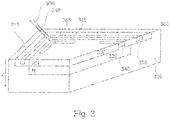
- Fig. 3 12 shows the cross section of a possible embodiment of a lateral Hall sensor 300 in CMOS technology with a sensitivity to the vertical magnetic field component (along the z-axis) and a silicon substrate 310.
- the functional layers of the Hall sensor 300 are located below the surface 315 of the silicon substrate 310 in respective doped regions 320, 330 of the semiconductor substrate 310.
- the first layer 320 in this embodiment is an n-type layer and the second layer 330 thereon is a p-type layer.
- the contacting of the Hall sensor 300 and other components in the silicon substrate 310 is effected by the further layer structure on the substrate by means of metal interconnects 340 and 350.
- the metal traces 340 and 350 contact the doping regions via respective contact diffusions 345 and 355.
- the Hall sensor 300 may also be formed as an array having a plurality of Hall elements connected together.
- the array may include lateral and vertical Hall elements that are sensitive to the vertical and horizontal magnetic field components, respectively.
- Magnetic field sensors such as TMR, AMR, etc. are usually mounted on the surface 315 of the semiconductor substrate 310.
- the teaching of this document also includes magnetic field sensors and other electronic components having an integrated component on the surface of a semiconductor substrate, which, among other things, extends into the semiconductor substrate 310 (as in CMOS technology, for example).
- the spinning current method is related to lateral Hall sensors 300 for suppressing the offset of the sensor signal from the book " Rotary Switch and Current Monitor by Hall-Based Microsystems "by Ralph Steiner Vanha, Physical Electronics Laboratory, Swiss Federal Institute of Technology (ETH) Zurich, 1999, pages 39-53 , known.
- the spinning current method consists of cyclically rotating the measurement and current direction on the Hall sensor 300 continuously at a specific clock frequency by, for example, 90 ° and summing over all measurement signals a full rotation through 360 ° and thereby the influence of offset To reduce voltages.
- the mechanical stress sensors themselves are subject to an undesired lateral dependence such as Temperature, which in turn must be compensated.
- the mechanical stress measurement in a semiconductor substrate is very complex and requires chip area ("real estate"), which is no longer available for other components, or which increases the current consumption and the production costs of the IC.
- An inaccuracy in the measured values also results from the fact that the mechanical stresses in the semiconductor substrate are measured at locations other than the mechanical stresses which are directly in the region in the case of the Hall sensors Act.
- the additional voltage measurements also require an increased processing effort of the measurement signals, which in turn is associated with a higher circuit complexity.
- Japanese Patent Application No. Hei. JP H09-97895 and Japanese Patent Application No. Hei. 2004-235328 describes a magnetic field sensor on or in a semiconductor substrate, wherein the magnetic field sensor is at least partially surrounded by a trench in a semiconductor substrate.
- the mechanical stress components in the semiconductor substrate in the region of the surface are largely avoided.
- the trench is only partially filled with the encapsulation material, cavities form, which can fill with water when the component is exposed to moisture.
- a sudden increase in temperature e.g. When soldering a packaged component arises, then leads to bursting of the shell (popcorn effect) and thus the destruction of the component.
- the trench and the magnetic field sensor are capped, with the magnetic field sensor at least partially framed by the trench and the trench completely penetrating the semiconductor substrate.
- the potting compound can no longer penetrate into the trench during the encapsulation process.
- the cap is adhesively bonded to the silicon Si substrate and may typically be in the range of the trench and the sensor element have a recess / cavity.
- Characterized in that the magnetic field sensor is at least partially surrounded by the trench an island in the semiconductor substrate is formed with the magnetic field sensor.
- a connection between a signal processing processor and the magnetic field sensor is provided on a connecting web between the island and the other part of the semiconductor substrate by interconnects running thereon or by highly conductive diffusions in the silicon substrate.
- the trench may first be filled with a suitable material, referred to hereinafter as buffer material.
- an additional layer of buffer material may be applied to the semiconductor substrate to absorb mechanical stresses acting between the sensor surface (island) and the potting compound.
- both said methods may also be combined, i.
- the cap can also be glued over a filled trench with / without buffer layer.
- the trench is produced in an embodiment, preferably by means of laser ablation.
- the removal can also be effected by means of a suitable physical dry etching process (reactive ion etching (RIE), deep reactive ion etching (Bosch process, DRIE), ion beam cutting), or by wet chemical etching using KOH or, for example, EDP.
- RIE reactive ion etching
- DRIE deep reactive ion etching
- ion beam cutting or by wet chemical etching using KOH or, for example, EDP.
- the trench has a depth, which z. B. at least one twentieth of the diagonal of the island on the surface or 5 microns. In another embodiment, the trench may completely penetrate the silicon substrate. The width of the trench is less than 100 microns, so that not too much silicon area is claimed.
- the trench is then filled with a filling material (buffer material).
- the magnetic field sensor may be a Hall sensor or another sensor which is sensitive to mechanical stresses.
- the island may also contain together with the Hall sensor several other components that have a cross-sensitivity to mechanical stresses and signal processing of / magnetic field sensors are needed, such as analog-to-digital converters or voltage and current sources for sensor supply.
- Fig. 1a shows a side view of a component 10 according to one aspect of this invention.
- a magnetic field sensor 30 is incorporated (integrated) in a semiconductor substrate 20 or disposed on a surface 25 of the semiconductor substrate 20.
- the magnetic field sensor 30 is at least partially surrounded by a trench 40.
- the trench 40 largely, but not completely, surrounds the electronic component 30, forming a kind of "island" 35 in the semiconductor substrate 20.
- a connecting web 50 leads between the island part of the surface 25 and the other part of the semiconductor substrate 20.
- the connecting web 50 extend metal interconnects 60 which connect the magnetic field sensor 30 on the island with other metal interconnects on the remaining part of the surface 25.
- a Hall sensor requires e.g. at least four lines 60 for the four connections or electronic connections.
- the electrical connections can also be realized by means of suitable diffusion on the connecting web instead of metal interconnects.
- the trench 40 has a depth t t which should be at least 5 ⁇ m or one twentieth of the diagonal H d of the island 35 on the surface 25.
- the trench 40 may also completely penetrate the semiconductor substrate 20.
- the trench 40 around the island 35 results in the magnetic field sensor 30 being largely isolated from stress forces in the semiconductor substrate 20.
- the magnetic field sensor 30 on the island 35 is thus not affected by the stress forces in the semiconductor substrate 20.
- the connecting web 50 does not have to run centrally on one side of the island in the trench 40.
- the connecting web 50 can also be arranged laterally, as seen from FIG. 2b can be seen. There may also be two connecting webs 50 (see Fig. 2d ).
- the trench 40 does not have to completely encircle the island 35 to achieve or propagate the desired isolation of the stress forces to prevent.
- Fig. 2e - 2h show, for example, aspects of the structure in which the trench 40 does not completely surround the island 35. Although the mechanical insulation in the aspects according to Fig. 2e - h not as strong as in other aspects, the fabrication of such trenches 40 can be achieved more cost effectively, and the island 35 is mechanically more robustly connected to the remainder of the semiconductor substrate 20.
- Fig. 2i - 2m show further embodiments of the trench 40, wherein in Fig. 2m the trench 40 is formed without a connecting web 50.
- the contacting of the electronic component can be made in this case, for example by bonding.
- the magnetic field sensor 30 can not only contain a single electronic component on its surface 25, but also has additional components 70.
- Fig. 2l shows another form of trench 40 with another component 70.
- Fig. 2p shows a possible embodiment with an island 35 at the edge of the semiconductor substrate 20 and
- Fig. 2n shows a possible embodiment with an island in a corner of the semiconductor substrate 20.
- the trench 40 is obtained by means of a conventional etching process, for example by laser ablation or other physical or wet chemical etching.
- etching processes come into consideration dry etching processes (reactive ion etching - RIE, deep reactive ion etching - Bosch process, DRIE and ion beam cutting), or wet chemical etching by means of KOH or EDP.
- the magnetic field sensor 30 and the other components are manufactured by conventional manufacturing steps.
- the trench 40 is in Fig. 1c optionally with one or more components for protection against external environmental influences partially lined on its inner surface (passivated).
- the lining layer 42 it is preferable to use a nitride such as Si 3 N 4 or a polyimide.
- the trench 40 is completely filled with or without lining, wherein the filling of the trench can also be done with several layers of different buffer materials.
- the buffer material (s) 45 typically has a smaller bulk modulus than the substrate.
- a buffer material is preferably a polymer such as an elastomer such as a Silicone compound or other suitable material which can absorb the occurring mechanical stresses in the filled trench.
- the buffer material may also be an epoxy resin.
- the filling of the trench 40 allows further encapsulation of the component, wherein no, or only small mechanical stresses are transmitted via the filling material 45 from the substrate to the island.
- a further buffer layer 46 may be grown on the surface 25 of the semiconductor substrate and the filled trench 40.
- This buffer layer absorbs the mechanical stresses which act on the potting compound on the surface of the island.
- the buffer layer typically covers at least the island as well as the trench and therefore only partially covers the entire Si surface.
- the buffer layer is made of the same material with which the trenches are filled.
- the buffer layer 46 may be applied from a plastic film by adhering to the surface 25. ( Fig. 1c shows a trench 40 with encapsulation layer 42 and buffer filling material 45 and buffer layer 46.)
- Fig. 1d shows an inventive component with cap 80 which is secured by means of an adhesive layer 81 above the island.
- the cap 80 includes an air volume 82 in its cavity.
- the cap protects the trench from ingress of material during the encapsulation process as well as moisture ingress and the formation of water reservoirs in the trench.
- the cap 80 may also be applied to a filled trench component with / without a buffer layer over the island surface.
- the cap 80 is typically made of a non-magnetic material. If a non-magnetic and electrically conductive material such as copper is used, the sensor element is additionally shielded from electromagnetic radiation.
- the component 10 in addition to the magnetic field sensor 30 and a plurality of magnetic field sensors, as well as circuit components that have a cross-sensitivity to mechanical stresses include and signal processing of / the magnetic field sensors are needed, such as Analog-to-digital converters or voltage and current sources for sensor supply.
Landscapes
- Physics & Mathematics (AREA)
- Condensed Matter Physics & Semiconductors (AREA)
- General Physics & Mathematics (AREA)
- Hall/Mr Elements (AREA)
- Measuring Magnetic Variables (AREA)
Claims (15)
- Composant (10) comprenant
un substrat semi-conducteur (20) avec une surface (25) ;
un capteur de champ magnétique (30) ; et
une tranchée (40) dans le substrat semi-conducteur (20), la tranchée entourant au moins partiellement le capteur de champ magnétique (30) et pénétrant complètement dans le substrat semi-conducteur (20),
caractérisé en ce que
la tranchée (40) et le capteur de champ magnétique (30) sont recouverts d'un capuchon (80). - Composant (10) selon la revendication 1, dans lequel la tranchée (40) est remplie d'un matériau de remplissage (45)
- Composant (10) selon la revendication 1 ou 2, dans lequel la surface (25) comprend une couche tampon (46).
- Composant (10) selon l'une quelconque des revendications 1 à 3, dans lequel la tranchée (40) entoure en grande partie le capteur de champ magnétique (30), afin de former un ilot (35), et a en outre un pont de liaison (50).
- Composant (10) selon la revendication 4, avec des pistes conductrices (60), des diffusions ou des liaisons de connexion, qui sont en contact avec des connexions électroniques du capteur de champ magnétique (30) et sont guidés sur / par le pont de liaison (50).
- Composant (10) selon l'une quelconque des revendications précédentes, dans lequel le capteur de champ magnétique (30) est intégré dans le substrat semi-conducteur (20).
- Composant (10) selon l'une quelconque des revendications précédentes, dans lequel le capteur de champ magnétique (30) est un capteur Hall.
- Composant (10) selon l'une quelconque des revendications précédentes, dans lequel la tranchée (40) a une profondeur (tt) qui est d'au moins 5 µm ou un vingtième de la diagonale (Hd) du capteur de champ magnétique (30).
- Composant (10) selon l'une quelconque des revendications précédentes, dans lequel la largeur (tb) de la tranchée (40) est inférieure à 100 µm.
- Composant (10) selon l'une quelconque des revendications précédentes, dans lequel le matériau de remplissage (45) est un polymère ou un polyimide.
- Composant (10) selon l'une quelconque des revendications précédentes, dans lequel la surface de la tranchée (40) comprend une couche d'encapsulation (42).
- Composant (10) selon la revendication 11, dans lequel la couche d'encapsulation (42) est un nitrure.
- Composant (10) selon l'une quelconque des revendications précédentes, dans lequel la tranchée (40) est produite par ablation au laser.
- Elément de construction (100) avec un composant (10) selon l'une quelconque des revendications précédentes, comprenant un autre composant (70) entouré au moins partiellement par la tranchée (40).
- Elément de construction (100) selon la revendication 14, dans lequel l'autre composant (70) est un composant de circuit pour commander le capteur de champ magnétique (30) ou pour capturer les données provenant du capteur de champ magnétique (30).
Applications Claiming Priority (2)
| Application Number | Priority Date | Filing Date | Title |
|---|---|---|---|
| DE102014111636 | 2014-08-14 | ||
| EP15170452.5A EP2985796B1 (fr) | 2014-08-14 | 2015-06-03 | Composants dotés de forces de contrainte réduites dans un substrat |
Related Parent Applications (2)
| Application Number | Title | Priority Date | Filing Date |
|---|---|---|---|
| EP15170452.5A Division-Into EP2985796B1 (fr) | 2014-08-14 | 2015-06-03 | Composants dotés de forces de contrainte réduites dans un substrat |
| EP15170452.5A Division EP2985796B1 (fr) | 2014-08-14 | 2015-06-03 | Composants dotés de forces de contrainte réduites dans un substrat |
Publications (2)
| Publication Number | Publication Date |
|---|---|
| EP3089228A1 EP3089228A1 (fr) | 2016-11-02 |
| EP3089228B1 true EP3089228B1 (fr) | 2019-11-27 |
Family
ID=53442480
Family Applications (2)
| Application Number | Title | Priority Date | Filing Date |
|---|---|---|---|
| EP15170452.5A Active EP2985796B1 (fr) | 2014-08-14 | 2015-06-03 | Composants dotés de forces de contrainte réduites dans un substrat |
| EP16167008.8A Active EP3089228B1 (fr) | 2014-08-14 | 2015-06-03 | Composants dotés de forces de contrainte réduites dans un substrat |
Family Applications Before (1)
| Application Number | Title | Priority Date | Filing Date |
|---|---|---|---|
| EP15170452.5A Active EP2985796B1 (fr) | 2014-08-14 | 2015-06-03 | Composants dotés de forces de contrainte réduites dans un substrat |
Country Status (1)
| Country | Link |
|---|---|
| EP (2) | EP2985796B1 (fr) |
Family Cites Families (7)
| Publication number | Priority date | Publication date | Assignee | Title |
|---|---|---|---|---|
| DE4137624A1 (de) | 1991-11-15 | 1993-05-19 | Bosch Gmbh Robert | Silizium-chip zur verwendung in einem kraftsensor |
| JP3471986B2 (ja) | 1995-09-29 | 2003-12-02 | 株式会社東芝 | ホール素子及びそれを用いた電力量計 |
| JP2004235328A (ja) | 2003-01-29 | 2004-08-19 | Denso Corp | ホール素子 |
| JP2005333103A (ja) * | 2004-03-30 | 2005-12-02 | Denso Corp | 縦型ホール素子およびその製造方法 |
| JP4674578B2 (ja) * | 2006-01-13 | 2011-04-20 | 株式会社デンソー | 磁気センサ及び磁気検出方法 |
| US7980138B2 (en) | 2007-10-29 | 2011-07-19 | Infineon Technologies Ag | Integrated circuit with stress sensing element |
| DE102011002580A1 (de) * | 2011-01-12 | 2012-07-12 | Fraunhofer-Gesellschaft zur Förderung der angewandten Forschung e.V. | Hall-Sensor und Verfahren zu dessen Herstellung |
-
2015
- 2015-06-03 EP EP15170452.5A patent/EP2985796B1/fr active Active
- 2015-06-03 EP EP16167008.8A patent/EP3089228B1/fr active Active
Non-Patent Citations (1)
| Title |
|---|
| None * |
Also Published As
| Publication number | Publication date |
|---|---|
| EP2985796B1 (fr) | 2017-11-01 |
| EP2985796A1 (fr) | 2016-02-17 |
| EP3089228A1 (fr) | 2016-11-02 |
Similar Documents
| Publication | Publication Date | Title |
|---|---|---|
| DE102014002991B4 (de) | Sensor-Gehäuse für die direkte Montage | |
| DE102006022336B4 (de) | Magnetfeldsensor und Sensoranordenung mit demselben | |
| DE102017205346B4 (de) | Drucksensor-package mit mehreren dies und dazugehöriges herstellungsverfahren | |
| DE102013222616B4 (de) | Mikromechanische Sensorvorrichtung | |
| DE102008042800A1 (de) | Vorrichtung zur Messung von Richtung und/oder Stärke eines Magnetfeldes | |
| EP3140245B1 (fr) | Composant de capteur à deux fonctions de détection | |
| DE102019117326A1 (de) | Mikroelektromechanische Struktur enthaltendes Halbleiterbauelement; MEMS-Sensor und Verfahren | |
| DE102009002559A1 (de) | Sensoranordnung | |
| WO2015185455A1 (fr) | Composant mems présentant une structure de découplage des contraintes et élément comprenant un composant mems de ce type | |
| DE102011053434A1 (de) | Bauteil zur Verwendung als doppelseitiges Sensorgehäuse | |
| DE102008015709A1 (de) | Elektrische Einrichtung mit Abdeckung | |
| WO2019016320A1 (fr) | Système de détection de pression et procédé de fabrication dudit système | |
| EP3167253B1 (fr) | Découplage de vibration de capteurs | |
| EP3089228B1 (fr) | Composants dotés de forces de contrainte réduites dans un substrat | |
| DE102006010484A1 (de) | Bewegungssensor | |
| DE102020202277A1 (de) | Mikromechanisches Bauteil für einen Stresssensor und Herstellungsverfahren für ein mikromechanisches Bauteil für einen Stresssensor | |
| DE112006001844B4 (de) | Verfahren zum Herstellen einer Elektronikkomponente und Elektronikkomponente | |
| WO2017005359A1 (fr) | Composant électrique et procédé de réalisation pour réaliser un tel composant électrique | |
| DE102012201458A1 (de) | Magnetoresistive vorrichtung und verfahren zum herstellen derselben | |
| DE102023204039A1 (de) | Membransensor zur Kompensation einer Beschleunigung und Verfahren zum Erzeugen eines kompensierten Sensorsignals | |
| DE102017128889A1 (de) | Magnetfeldsensor | |
| DE102015206299B4 (de) | Über Leiterplatte auf Leadframe verschaltete Sensorschaltung | |
| DE102021204645A1 (de) | Verfahren zur Herstellung eines mikroelektromechanischen Sensors aus einem MEMS-Element und einem ASIC-Element und mikroelektromechanischer Sensor | |
| DE102014223850A1 (de) | Mikromechanische Sensorvorrichtung und entsprechendes Herstellungsverfahren | |
| WO2017220319A1 (fr) | Ensemble comprenant un support et un corps de boîtier, et procédé de fabrication d'un ensemble comprenant un élément structural |
Legal Events
| Date | Code | Title | Description |
|---|---|---|---|
| PUAI | Public reference made under article 153(3) epc to a published international application that has entered the european phase |
Free format text: ORIGINAL CODE: 0009012 |
|
| AC | Divisional application: reference to earlier application |
Ref document number: 2985796 Country of ref document: EP Kind code of ref document: P |
|
| AK | Designated contracting states |
Kind code of ref document: A1 Designated state(s): AL AT BE BG CH CY CZ DE DK EE ES FI FR GB GR HR HU IE IS IT LI LT LU LV MC MK MT NL NO PL PT RO RS SE SI SK SM TR |
|
| AX | Request for extension of the european patent |
Extension state: BA ME |
|
| RAP1 | Party data changed (applicant data changed or rights of an application transferred) |
Owner name: TDK-MICRONAS GMBH |
|
| STAA | Information on the status of an ep patent application or granted ep patent |
Free format text: STATUS: REQUEST FOR EXAMINATION WAS MADE |
|
| 17P | Request for examination filed |
Effective date: 20170502 |
|
| RBV | Designated contracting states (corrected) |
Designated state(s): AL AT BE BG CH CY CZ DE DK EE ES FI FR GB GR HR HU IE IS IT LI LT LU LV MC MK MT NL NO PL PT RO RS SE SI SK SM TR |
|
| R17P | Request for examination filed (corrected) |
Effective date: 20170323 |
|
| RBV | Designated contracting states (corrected) |
Designated state(s): AL AT BE BG CH CY CZ DE DK EE ES FI FR GB GR HR HU IE IS IT LI LT LU LV MC MK MT NL NO PL PT RO RS SE SI SK SM TR |
|
| STAA | Information on the status of an ep patent application or granted ep patent |
Free format text: STATUS: EXAMINATION IS IN PROGRESS |
|
| 17Q | First examination report despatched |
Effective date: 20171130 |
|
| GRAP | Despatch of communication of intention to grant a patent |
Free format text: ORIGINAL CODE: EPIDOSNIGR1 |
|
| STAA | Information on the status of an ep patent application or granted ep patent |
Free format text: STATUS: GRANT OF PATENT IS INTENDED |
|
| INTG | Intention to grant announced |
Effective date: 20181204 |
|
| GRAJ | Information related to disapproval of communication of intention to grant by the applicant or resumption of examination proceedings by the epo deleted |
Free format text: ORIGINAL CODE: EPIDOSDIGR1 |
|
| STAA | Information on the status of an ep patent application or granted ep patent |
Free format text: STATUS: EXAMINATION IS IN PROGRESS |
|
| INTC | Intention to grant announced (deleted) | ||
| GRAP | Despatch of communication of intention to grant a patent |
Free format text: ORIGINAL CODE: EPIDOSNIGR1 |
|
| STAA | Information on the status of an ep patent application or granted ep patent |
Free format text: STATUS: GRANT OF PATENT IS INTENDED |
|
| INTG | Intention to grant announced |
Effective date: 20190621 |
|
| GRAS | Grant fee paid |
Free format text: ORIGINAL CODE: EPIDOSNIGR3 |
|
| GRAA | (expected) grant |
Free format text: ORIGINAL CODE: 0009210 |
|
| STAA | Information on the status of an ep patent application or granted ep patent |
Free format text: STATUS: THE PATENT HAS BEEN GRANTED |
|
| AC | Divisional application: reference to earlier application |
Ref document number: 2985796 Country of ref document: EP Kind code of ref document: P |
|
| AK | Designated contracting states |
Kind code of ref document: B1 Designated state(s): AL AT BE BG CH CY CZ DE DK EE ES FI FR GB GR HR HU IE IS IT LI LT LU LV MC MK MT NL NO PL PT RO RS SE SI SK SM TR |
|
| REG | Reference to a national code |
Ref country code: GB Ref legal event code: FG4D Free format text: NOT ENGLISH |
|
| REG | Reference to a national code |
Ref country code: CH Ref legal event code: EP |
|
| REG | Reference to a national code |
Ref country code: AT Ref legal event code: REF Ref document number: 1207705 Country of ref document: AT Kind code of ref document: T Effective date: 20191215 |
|
| REG | Reference to a national code |
Ref country code: DE Ref legal event code: R096 Ref document number: 502015011093 Country of ref document: DE |
|
| REG | Reference to a national code |
Ref country code: IE Ref legal event code: FG4D Free format text: LANGUAGE OF EP DOCUMENT: GERMAN |
|
| REG | Reference to a national code |
Ref country code: NL Ref legal event code: MP Effective date: 20191127 |
|
| REG | Reference to a national code |
Ref country code: LT Ref legal event code: MG4D |
|
| PG25 | Lapsed in a contracting state [announced via postgrant information from national office to epo] |
Ref country code: NO Free format text: LAPSE BECAUSE OF FAILURE TO SUBMIT A TRANSLATION OF THE DESCRIPTION OR TO PAY THE FEE WITHIN THE PRESCRIBED TIME-LIMIT Effective date: 20200227 Ref country code: GR Free format text: LAPSE BECAUSE OF FAILURE TO SUBMIT A TRANSLATION OF THE DESCRIPTION OR TO PAY THE FEE WITHIN THE PRESCRIBED TIME-LIMIT Effective date: 20200228 Ref country code: LT Free format text: LAPSE BECAUSE OF FAILURE TO SUBMIT A TRANSLATION OF THE DESCRIPTION OR TO PAY THE FEE WITHIN THE PRESCRIBED TIME-LIMIT Effective date: 20191127 Ref country code: SE Free format text: LAPSE BECAUSE OF FAILURE TO SUBMIT A TRANSLATION OF THE DESCRIPTION OR TO PAY THE FEE WITHIN THE PRESCRIBED TIME-LIMIT Effective date: 20191127 Ref country code: LV Free format text: LAPSE BECAUSE OF FAILURE TO SUBMIT A TRANSLATION OF THE DESCRIPTION OR TO PAY THE FEE WITHIN THE PRESCRIBED TIME-LIMIT Effective date: 20191127 Ref country code: NL Free format text: LAPSE BECAUSE OF FAILURE TO SUBMIT A TRANSLATION OF THE DESCRIPTION OR TO PAY THE FEE WITHIN THE PRESCRIBED TIME-LIMIT Effective date: 20191127 Ref country code: FI Free format text: LAPSE BECAUSE OF FAILURE TO SUBMIT A TRANSLATION OF THE DESCRIPTION OR TO PAY THE FEE WITHIN THE PRESCRIBED TIME-LIMIT Effective date: 20191127 Ref country code: BG Free format text: LAPSE BECAUSE OF FAILURE TO SUBMIT A TRANSLATION OF THE DESCRIPTION OR TO PAY THE FEE WITHIN THE PRESCRIBED TIME-LIMIT Effective date: 20200227 |
|
| PG25 | Lapsed in a contracting state [announced via postgrant information from national office to epo] |
Ref country code: RS Free format text: LAPSE BECAUSE OF FAILURE TO SUBMIT A TRANSLATION OF THE DESCRIPTION OR TO PAY THE FEE WITHIN THE PRESCRIBED TIME-LIMIT Effective date: 20191127 Ref country code: HR Free format text: LAPSE BECAUSE OF FAILURE TO SUBMIT A TRANSLATION OF THE DESCRIPTION OR TO PAY THE FEE WITHIN THE PRESCRIBED TIME-LIMIT Effective date: 20191127 Ref country code: IS Free format text: LAPSE BECAUSE OF FAILURE TO SUBMIT A TRANSLATION OF THE DESCRIPTION OR TO PAY THE FEE WITHIN THE PRESCRIBED TIME-LIMIT Effective date: 20200327 |
|
| PG25 | Lapsed in a contracting state [announced via postgrant information from national office to epo] |
Ref country code: AL Free format text: LAPSE BECAUSE OF FAILURE TO SUBMIT A TRANSLATION OF THE DESCRIPTION OR TO PAY THE FEE WITHIN THE PRESCRIBED TIME-LIMIT Effective date: 20191127 |
|
| PG25 | Lapsed in a contracting state [announced via postgrant information from national office to epo] |
Ref country code: EE Free format text: LAPSE BECAUSE OF FAILURE TO SUBMIT A TRANSLATION OF THE DESCRIPTION OR TO PAY THE FEE WITHIN THE PRESCRIBED TIME-LIMIT Effective date: 20191127 Ref country code: PT Free format text: LAPSE BECAUSE OF FAILURE TO SUBMIT A TRANSLATION OF THE DESCRIPTION OR TO PAY THE FEE WITHIN THE PRESCRIBED TIME-LIMIT Effective date: 20200419 Ref country code: DK Free format text: LAPSE BECAUSE OF FAILURE TO SUBMIT A TRANSLATION OF THE DESCRIPTION OR TO PAY THE FEE WITHIN THE PRESCRIBED TIME-LIMIT Effective date: 20191127 Ref country code: RO Free format text: LAPSE BECAUSE OF FAILURE TO SUBMIT A TRANSLATION OF THE DESCRIPTION OR TO PAY THE FEE WITHIN THE PRESCRIBED TIME-LIMIT Effective date: 20191127 Ref country code: CZ Free format text: LAPSE BECAUSE OF FAILURE TO SUBMIT A TRANSLATION OF THE DESCRIPTION OR TO PAY THE FEE WITHIN THE PRESCRIBED TIME-LIMIT Effective date: 20191127 Ref country code: ES Free format text: LAPSE BECAUSE OF FAILURE TO SUBMIT A TRANSLATION OF THE DESCRIPTION OR TO PAY THE FEE WITHIN THE PRESCRIBED TIME-LIMIT Effective date: 20191127 |
|
| PGFP | Annual fee paid to national office [announced via postgrant information from national office to epo] |
Ref country code: FR Payment date: 20200619 Year of fee payment: 6 |
|
| REG | Reference to a national code |
Ref country code: DE Ref legal event code: R097 Ref document number: 502015011093 Country of ref document: DE |
|
| PG25 | Lapsed in a contracting state [announced via postgrant information from national office to epo] |
Ref country code: SM Free format text: LAPSE BECAUSE OF FAILURE TO SUBMIT A TRANSLATION OF THE DESCRIPTION OR TO PAY THE FEE WITHIN THE PRESCRIBED TIME-LIMIT Effective date: 20191127 Ref country code: SK Free format text: LAPSE BECAUSE OF FAILURE TO SUBMIT A TRANSLATION OF THE DESCRIPTION OR TO PAY THE FEE WITHIN THE PRESCRIBED TIME-LIMIT Effective date: 20191127 |
|
| PGFP | Annual fee paid to national office [announced via postgrant information from national office to epo] |
Ref country code: GB Payment date: 20200625 Year of fee payment: 6 |
|
| PLBE | No opposition filed within time limit |
Free format text: ORIGINAL CODE: 0009261 |
|
| STAA | Information on the status of an ep patent application or granted ep patent |
Free format text: STATUS: NO OPPOSITION FILED WITHIN TIME LIMIT |
|
| 26N | No opposition filed |
Effective date: 20200828 |
|
| PG25 | Lapsed in a contracting state [announced via postgrant information from national office to epo] |
Ref country code: PL Free format text: LAPSE BECAUSE OF FAILURE TO SUBMIT A TRANSLATION OF THE DESCRIPTION OR TO PAY THE FEE WITHIN THE PRESCRIBED TIME-LIMIT Effective date: 20191127 Ref country code: SI Free format text: LAPSE BECAUSE OF FAILURE TO SUBMIT A TRANSLATION OF THE DESCRIPTION OR TO PAY THE FEE WITHIN THE PRESCRIBED TIME-LIMIT Effective date: 20191127 |
|
| REG | Reference to a national code |
Ref country code: DE Ref legal event code: R082 Ref document number: 502015011093 Country of ref document: DE Representative=s name: SONNENBERG HARRISON PARTNERSCHAFT MBB, DE Ref country code: DE Ref legal event code: R082 Ref document number: 502015011093 Country of ref document: DE Representative=s name: SONNENBERG HARRISON PARTNERSCHAFT MBB PATENT- , DE |
|
| REG | Reference to a national code |
Ref country code: DE Ref legal event code: R082 Ref document number: 502015011093 Country of ref document: DE Representative=s name: SONNENBERG HARRISON PARTNERSCHAFT MBB, DE |
|
| PG25 | Lapsed in a contracting state [announced via postgrant information from national office to epo] |
Ref country code: MC Free format text: LAPSE BECAUSE OF FAILURE TO SUBMIT A TRANSLATION OF THE DESCRIPTION OR TO PAY THE FEE WITHIN THE PRESCRIBED TIME-LIMIT Effective date: 20191127 Ref country code: IT Free format text: LAPSE BECAUSE OF FAILURE TO SUBMIT A TRANSLATION OF THE DESCRIPTION OR TO PAY THE FEE WITHIN THE PRESCRIBED TIME-LIMIT Effective date: 20191127 |
|
| REG | Reference to a national code |
Ref country code: CH Ref legal event code: PL |
|
| PG25 | Lapsed in a contracting state [announced via postgrant information from national office to epo] |
Ref country code: LU Free format text: LAPSE BECAUSE OF NON-PAYMENT OF DUE FEES Effective date: 20200603 |
|
| REG | Reference to a national code |
Ref country code: BE Ref legal event code: MM Effective date: 20200630 |
|
| PG25 | Lapsed in a contracting state [announced via postgrant information from national office to epo] |
Ref country code: IE Free format text: LAPSE BECAUSE OF NON-PAYMENT OF DUE FEES Effective date: 20200603 Ref country code: CH Free format text: LAPSE BECAUSE OF NON-PAYMENT OF DUE FEES Effective date: 20200630 Ref country code: LI Free format text: LAPSE BECAUSE OF NON-PAYMENT OF DUE FEES Effective date: 20200630 |
|
| PG25 | Lapsed in a contracting state [announced via postgrant information from national office to epo] |
Ref country code: BE Free format text: LAPSE BECAUSE OF NON-PAYMENT OF DUE FEES Effective date: 20200630 |
|
| REG | Reference to a national code |
Ref country code: AT Ref legal event code: MM01 Ref document number: 1207705 Country of ref document: AT Kind code of ref document: T Effective date: 20200603 |
|
| PG25 | Lapsed in a contracting state [announced via postgrant information from national office to epo] |
Ref country code: AT Free format text: LAPSE BECAUSE OF NON-PAYMENT OF DUE FEES Effective date: 20200603 |
|
| GBPC | Gb: european patent ceased through non-payment of renewal fee |
Effective date: 20210603 |
|
| PG25 | Lapsed in a contracting state [announced via postgrant information from national office to epo] |
Ref country code: GB Free format text: LAPSE BECAUSE OF NON-PAYMENT OF DUE FEES Effective date: 20210603 |
|
| PG25 | Lapsed in a contracting state [announced via postgrant information from national office to epo] |
Ref country code: TR Free format text: LAPSE BECAUSE OF FAILURE TO SUBMIT A TRANSLATION OF THE DESCRIPTION OR TO PAY THE FEE WITHIN THE PRESCRIBED TIME-LIMIT Effective date: 20191127 Ref country code: MT Free format text: LAPSE BECAUSE OF FAILURE TO SUBMIT A TRANSLATION OF THE DESCRIPTION OR TO PAY THE FEE WITHIN THE PRESCRIBED TIME-LIMIT Effective date: 20191127 Ref country code: FR Free format text: LAPSE BECAUSE OF NON-PAYMENT OF DUE FEES Effective date: 20210630 Ref country code: CY Free format text: LAPSE BECAUSE OF FAILURE TO SUBMIT A TRANSLATION OF THE DESCRIPTION OR TO PAY THE FEE WITHIN THE PRESCRIBED TIME-LIMIT Effective date: 20191127 |
|
| PG25 | Lapsed in a contracting state [announced via postgrant information from national office to epo] |
Ref country code: MK Free format text: LAPSE BECAUSE OF FAILURE TO SUBMIT A TRANSLATION OF THE DESCRIPTION OR TO PAY THE FEE WITHIN THE PRESCRIBED TIME-LIMIT Effective date: 20191127 |
|
| REG | Reference to a national code |
Ref country code: DE Ref legal event code: R079 Ref document number: 502015011093 Country of ref document: DE Free format text: PREVIOUS MAIN CLASS: H01L0043060000 Ipc: H10N0052000000 |
|
| P01 | Opt-out of the competence of the unified patent court (upc) registered |
Effective date: 20231130 |
|
| PGFP | Annual fee paid to national office [announced via postgrant information from national office to epo] |
Ref country code: DE Payment date: 20250618 Year of fee payment: 11 |