EP3089562A1 - Verarbeitungsverfahren für leiterplatte und leiterplatte - Google Patents
Verarbeitungsverfahren für leiterplatte und leiterplatte Download PDFInfo
- Publication number
- EP3089562A1 EP3089562A1 EP14875182.9A EP14875182A EP3089562A1 EP 3089562 A1 EP3089562 A1 EP 3089562A1 EP 14875182 A EP14875182 A EP 14875182A EP 3089562 A1 EP3089562 A1 EP 3089562A1
- Authority
- EP
- European Patent Office
- Prior art keywords
- pcb
- hole
- connector
- present
- blind hole
- Prior art date
- Legal status (The legal status is an assumption and is not a legal conclusion. Google has not performed a legal analysis and makes no representation as to the accuracy of the status listed.)
- Granted
Links
Images



Classifications
-
- H—ELECTRICITY
- H05—ELECTRIC TECHNIQUES NOT OTHERWISE PROVIDED FOR
- H05K—PRINTED CIRCUITS; CASINGS OR CONSTRUCTIONAL DETAILS OF ELECTRIC APPARATUS; MANUFACTURE OF ASSEMBLAGES OF ELECTRICAL COMPONENTS
- H05K3/00—Apparatus or processes for manufacturing printed circuits
- H05K3/46—Manufacturing multilayer circuits
- H05K3/4611—Manufacturing multilayer circuits by laminating two or more circuit boards
-
- H—ELECTRICITY
- H05—ELECTRIC TECHNIQUES NOT OTHERWISE PROVIDED FOR
- H05K—PRINTED CIRCUITS; CASINGS OR CONSTRUCTIONAL DETAILS OF ELECTRIC APPARATUS; MANUFACTURE OF ASSEMBLAGES OF ELECTRICAL COMPONENTS
- H05K3/00—Apparatus or processes for manufacturing printed circuits
- H05K3/40—Forming printed elements for providing electric connections to or between printed circuits
- H05K3/42—Plated through-holes or plated via connections
- H05K3/429—Plated through-holes specially for multilayer circuits, e.g. having connections to inner circuit layers
-
- H—ELECTRICITY
- H05—ELECTRIC TECHNIQUES NOT OTHERWISE PROVIDED FOR
- H05K—PRINTED CIRCUITS; CASINGS OR CONSTRUCTIONAL DETAILS OF ELECTRIC APPARATUS; MANUFACTURE OF ASSEMBLAGES OF ELECTRICAL COMPONENTS
- H05K1/00—Printed circuits
- H05K1/02—Details
- H05K1/0296—Conductive pattern lay-out details not covered by sub groups H05K1/02 - H05K1/0295
- H05K1/0298—Multilayer circuits
-
- H—ELECTRICITY
- H05—ELECTRIC TECHNIQUES NOT OTHERWISE PROVIDED FOR
- H05K—PRINTED CIRCUITS; CASINGS OR CONSTRUCTIONAL DETAILS OF ELECTRIC APPARATUS; MANUFACTURE OF ASSEMBLAGES OF ELECTRICAL COMPONENTS
- H05K1/00—Printed circuits
- H05K1/02—Details
- H05K1/09—Use of materials for the conductive, e.g. metallic pattern
-
- H—ELECTRICITY
- H05—ELECTRIC TECHNIQUES NOT OTHERWISE PROVIDED FOR
- H05K—PRINTED CIRCUITS; CASINGS OR CONSTRUCTIONAL DETAILS OF ELECTRIC APPARATUS; MANUFACTURE OF ASSEMBLAGES OF ELECTRICAL COMPONENTS
- H05K1/00—Printed circuits
- H05K1/02—Details
- H05K1/11—Printed elements for providing electric connections to or between printed circuits
- H05K1/115—Via connections; Lands around holes or via connections
-
- H—ELECTRICITY
- H05—ELECTRIC TECHNIQUES NOT OTHERWISE PROVIDED FOR
- H05K—PRINTED CIRCUITS; CASINGS OR CONSTRUCTIONAL DETAILS OF ELECTRIC APPARATUS; MANUFACTURE OF ASSEMBLAGES OF ELECTRICAL COMPONENTS
- H05K3/00—Apparatus or processes for manufacturing printed circuits
- H05K3/0011—Working of insulating substrates or insulating layers
- H05K3/0044—Mechanical working of the substrate, e.g. drilling or punching
- H05K3/0047—Drilling of holes
-
- H—ELECTRICITY
- H05—ELECTRIC TECHNIQUES NOT OTHERWISE PROVIDED FOR
- H05K—PRINTED CIRCUITS; CASINGS OR CONSTRUCTIONAL DETAILS OF ELECTRIC APPARATUS; MANUFACTURE OF ASSEMBLAGES OF ELECTRICAL COMPONENTS
- H05K3/00—Apparatus or processes for manufacturing printed circuits
- H05K3/40—Forming printed elements for providing electric connections to or between printed circuits
- H05K3/42—Plated through-holes or plated via connections
- H05K3/423—Plated through-holes or plated via connections characterised by electroplating method
- H05K3/424—Plated through-holes or plated via connections characterised by electroplating method by direct electroplating
-
- H—ELECTRICITY
- H05—ELECTRIC TECHNIQUES NOT OTHERWISE PROVIDED FOR
- H05K—PRINTED CIRCUITS; CASINGS OR CONSTRUCTIONAL DETAILS OF ELECTRIC APPARATUS; MANUFACTURE OF ASSEMBLAGES OF ELECTRICAL COMPONENTS
- H05K3/00—Apparatus or processes for manufacturing printed circuits
- H05K3/46—Manufacturing multilayer circuits
- H05K3/4611—Manufacturing multilayer circuits by laminating two or more circuit boards
- H05K3/4623—Manufacturing multilayer circuits by laminating two or more circuit boards the circuit boards having internal via connections between two or more circuit layers before lamination, e.g. double-sided circuit boards
-
- H—ELECTRICITY
- H05—ELECTRIC TECHNIQUES NOT OTHERWISE PROVIDED FOR
- H05K—PRINTED CIRCUITS; CASINGS OR CONSTRUCTIONAL DETAILS OF ELECTRIC APPARATUS; MANUFACTURE OF ASSEMBLAGES OF ELECTRICAL COMPONENTS
- H05K2201/00—Indexing scheme relating to printed circuits covered by H05K1/00
- H05K2201/10—Details of components or other objects attached to or integrated in a printed circuit board
- H05K2201/10227—Other objects, e.g. metallic pieces
- H05K2201/10295—Metallic connector elements partly mounted in a hole of the PCB
- H05K2201/10303—Pin-in-hole mounted pins
-
- H—ELECTRICITY
- H05—ELECTRIC TECHNIQUES NOT OTHERWISE PROVIDED FOR
- H05K—PRINTED CIRCUITS; CASINGS OR CONSTRUCTIONAL DETAILS OF ELECTRIC APPARATUS; MANUFACTURE OF ASSEMBLAGES OF ELECTRICAL COMPONENTS
- H05K2203/00—Indexing scheme relating to apparatus or processes for manufacturing printed circuits covered by H05K3/00
- H05K2203/02—Details related to mechanical or acoustic processing, e.g. drilling, punching, cutting, using ultrasound
- H05K2203/0207—Partly drilling through substrate until a controlled depth, e.g. with end-point detection
-
- H—ELECTRICITY
- H05—ELECTRIC TECHNIQUES NOT OTHERWISE PROVIDED FOR
- H05K—PRINTED CIRCUITS; CASINGS OR CONSTRUCTIONAL DETAILS OF ELECTRIC APPARATUS; MANUFACTURE OF ASSEMBLAGES OF ELECTRICAL COMPONENTS
- H05K2203/00—Indexing scheme relating to apparatus or processes for manufacturing printed circuits covered by H05K3/00
- H05K2203/16—Inspection; Monitoring; Aligning
Definitions
- the present invention relates to the field of PCB technologies, and in particular, to a PCB processing method and a PCB.
- PCB printed circuit boards
- connectors is widely used in a communication system to implement the transmission of inter-board signals.
- the capacity of a typical switching system reaches 10T, and up to hundreds of connectors are used.
- Very high requirements for the density of the connectors and the rate of single channels are proposed because very high communication capacity needs to be met and so many single boards and connectors need to be installed in a cabinet having a limited space.
- the single channel rate of the connectors has been raised more than 25Gbps, and the minimum distance between connector wafers is only 1.85mm.
- the density of the connectors has to be reduced to further improve the single channel rate of the connectors.
- the density and rate of the connectors are actually contradictory.
- a through hole is generally designed on a PCB for crimping the connectors.
- the wiring space of the PCB is limited by the space between wafers.
- the present invention is proposed to provide a PCB processing method and a PCB for overcoming the aforementioned problems or at least in part solving the aforementioned problems.
- the present invention provides a PCB processing method, including: respectively carrying out lamination processing on a plurality of PCB daughter boards constituting a PCB according to PCB design requirements, and drilling and electroplating a top-most PCB daughter board of the PCB to form a via hole; laminating the plurality of PCB daughter boards together to form the PCB, and drilling and electroplating the formed PCB to form a through hole for mounting a connector, wherein a depth of the blind hole is greater than or equal to a length of a signal pin of the connector.
- the method further includes: backdrilling the via hole that needs to be backdrilled.
- the blind hole has a metallized part after backdrilling, and a length of the metallized part is greater than or equal to that of the signal pin of the connector.
- drilling and electroplating the formed PCB to form a through hole for mounting the connector includes: drilling and electroplating the formed PCB at preset intervals to form multiple through holes for mounting connectors.
- the method further includes: backdrilling the through hole that needs to be backdrilled.
- the method further includes: determining a position of the through hole and of the blind hole according to wiring pattern of the PCB.
- the top-most PCB daughter board is formed by laminating a core board and a dielectric.
- the bottom-most PCB daughter board of the plurality of PCB daughter boards constituting the PCB is formed by directly processing a core board or is formed by the core board and a dielectric.
- the present invention further provides a PCB fabricated by the foregoing printed circuit board PCB processing method, the PCB is formed by laminating multilayer PCB daughter boards, and the PCB is provided with a blind hole and a through hole for mounting a connector.
- the blind hole and the through hole are backdrilled.
- the embodiments of the present invention provide a printed circuit board PCB processing method and a PCB, which may enable the space for layout between wafers to be doubled without reducing the density of the connector. Furthermore, the stub in the crimping of the blind hole may be effectively reduced by adopting multiple backdrilling before crimping.
- FIG. 1 is a flowchart of a PCB processing method according to the embodiments of the present invention.
- the PCB processing method according to the embodiments of the present invention includes processing in the following Step 101 to Step 102.
- Step 101 lamination processing is respectively carried out on a plurality of PCB daughter boards constituting a PCB according to PCB design requirements, and a top-most PCB daughter board of the PCB is drilled and electroplated to form a via hole, where the top-most PCB daughter board is formed by laminating a core board and a dielectric.
- a bottom-most PCB daughter board of the plurality of PCB daughter boards constituting the PCB is formed by directly processing a core board or is formed by laminating the core board and a dielectric.
- the blind hole has a metallized part after backdrilling, and a length of the metallized part is greater than or equal to that of the signal pin of the connector.
- Step 102 the plurality of PCB daughter boards are laminated together to form the PCB, and the formed PCB is drilled and electroplated to form a through hole for mounting the connector, wherein a blind hole for mounting a connector is formed by the via hole, and a depth of the blind hole is greater than or equal to a length of the signal pin of the connector.
- the formed PCB may be drilled and electroplated at preset intervals to form multiple through holes for mounting connectors. And the through hole that needs to be backdrilled may be backdrilled.
- a position of the through hole and of the blind hole may be determined according to the wiring pattern of the PCB.
- the connector may be crimped by using the blind hole every other wafer.
- the embodiments of the present invention propose a PCB processing method for connector crimping.
- the blind hole is formed by twice or more laminations. And where in terms of design and processing, it is needed to guarantee that the depth of the blind hole is greater than the length of the signal pin of the connector, so as to guarantee that the connector may be inserted from the blind hole by crimping.
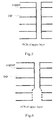
- a crimping effect after processing is as shown in FIG. 2 .
- the backdrilling of the PCB of upper layer needs to be carried out before laminating, the blind hole has a metallized part after backdrilling, and a length of the metallized part is greater than that of the signal pin of the connector, which guarantees that the connector may be inserted from the blind hole by crimping.
- the backdrilling of the lower layer of PCB is carried out upon completion of laminating of the PCB of upper layer and PCB of lower layer.
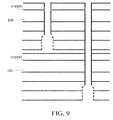
- the crimping effect after processing is as shown in FIG. 3 . If the wiring space needs to be further increased, one through hole may be formed every other two rows, or the position of the through hole and of the blind hole may be freely deployed according to the wiring pattern to achieve the optimum wiring effect.
- the connector may be assembled, and the schematic diagram after assembly is as shown in FIG. 2 and FIG. 3 .
- wafers between lower layer of PCB may be doubled via reasonably designing the crimping of PCB and connectors, namely by means of twice or more laminations, so that the wiring space between wafers may be doubled.
- the blind hole is backdrilled before multiple laminating, which may effectively reduce the length of the stub.
- the PCB fabricated by the foregoing PCB processing method, as shown in FIG. 2 or FIG. 3
- the PCB according to the embodiments of the present invention is formed by laminating multilayer PCB daughter boards, and the PCB is provided with a blind hole and a through hole for mounting a connector.
- the blind hole and the through hole are the backdrilled blind hole and backdrilled through hole.
- wafers between lower layer of PCB may be doubled via considerable designing the crimping of PCB and connectors, namely by means of twice or more laminations, so that the wiring space between wafers may be doubled.
- the blind hole is backdrilled before multiple laminating, which may effectively reduce the length of the stub.
- wafers between lower layer of PCB may be doubled via forming the blind hole by twice or more laminations, so that the wring space between wafers may be doubled. Furthermore, the stub in the crimping of the blind hole may be effectively reduced by backdrilling before multiple laminating. Therefore, the present invention has industrial applicability
Landscapes
- Engineering & Computer Science (AREA)
- Microelectronics & Electronic Packaging (AREA)
- Manufacturing & Machinery (AREA)
- Printing Elements For Providing Electric Connections Between Printed Circuits (AREA)
- Production Of Multi-Layered Print Wiring Board (AREA)
Applications Claiming Priority (2)
| Application Number | Priority Date | Filing Date | Title |
|---|---|---|---|
| CN201310739302.6A CN104754886B (zh) | 2013-12-27 | 2013-12-27 | Pcb加工方法及pcb |
| PCT/CN2014/078052 WO2015096365A1 (zh) | 2013-12-27 | 2014-05-21 | Pcb加工方法及pcb |
Publications (3)
| Publication Number | Publication Date |
|---|---|
| EP3089562A1 true EP3089562A1 (de) | 2016-11-02 |
| EP3089562A4 EP3089562A4 (de) | 2017-10-11 |
| EP3089562B1 EP3089562B1 (de) | 2022-07-13 |
Family
ID=53477447
Family Applications (1)
| Application Number | Title | Priority Date | Filing Date |
|---|---|---|---|
| EP14875182.9A Active EP3089562B1 (de) | 2013-12-27 | 2014-05-21 | Verarbeitungsverfahren für leiterplatte und leiterplatte |
Country Status (4)
| Country | Link |
|---|---|
| US (1) | US10064271B2 (de) |
| EP (1) | EP3089562B1 (de) |
| CN (1) | CN104754886B (de) |
| WO (1) | WO2015096365A1 (de) |
Cited By (2)
| Publication number | Priority date | Publication date | Assignee | Title |
|---|---|---|---|---|
| WO2018175660A1 (en) * | 2017-03-21 | 2018-09-27 | Sanmina Corporation | Methods of forming blind vias for printed circuit boards |
| CN110839320A (zh) * | 2019-11-21 | 2020-02-25 | 星河电路(福建)有限公司 | 沉头孔类pcb板的加工方法 |
Families Citing this family (16)
| Publication number | Priority date | Publication date | Assignee | Title |
|---|---|---|---|---|
| JP2016213136A (ja) * | 2015-05-13 | 2016-12-15 | 富士通株式会社 | 配線基板、電子装置および配線基板の製造方法 |
| CN106559960B (zh) * | 2015-09-29 | 2020-11-06 | 中兴通讯股份有限公司 | 双面阶梯孔电路板及其实现方法 |
| CN107072050B (zh) * | 2017-03-30 | 2019-05-07 | 生益电子股份有限公司 | Pcb上插孔的制作方法及pcb |
| CN106961790A (zh) * | 2017-04-20 | 2017-07-18 | 广东浪潮大数据研究有限公司 | 一种多层pcb及其制作方法 |
| US11177590B2 (en) | 2017-06-19 | 2021-11-16 | Intel Corporation | Printed circuit board with a connector for electric connection of the PCB with another apparatus |
| US10856414B2 (en) | 2018-03-12 | 2020-12-01 | Dell Products, L.P. | System and method for minimizing connector pad open-circuit stubs |
| CN108966568B (zh) * | 2018-07-26 | 2020-11-13 | 维沃移动通信有限公司 | 一种电子设备 |
| CN111278238B (zh) * | 2018-12-05 | 2023-06-06 | 中兴通讯股份有限公司 | 双面压接背板及其生产方法 |
| CN110730558B (zh) * | 2019-09-09 | 2021-02-12 | 华为机器有限公司 | 印刷电路板及通信设备 |
| CN110740591B (zh) * | 2019-10-25 | 2021-06-25 | 珠海杰赛科技有限公司 | 一种多层印制板的盲孔加工方法 |
| CN114258194B (zh) * | 2020-09-24 | 2025-07-18 | 深南电路股份有限公司 | 一种电路板及其制造方法 |
| CN112328554B (zh) * | 2020-11-23 | 2022-09-13 | 迈普通信技术股份有限公司 | 生成二次钻孔文件的方法、装置、电子设备及存储介质 |
| CN112888199A (zh) * | 2021-01-15 | 2021-06-01 | 浪潮电子信息产业股份有限公司 | 一种多层pcb板引脚插孔开设方法 |
| CN113939082B (zh) * | 2021-09-18 | 2023-02-07 | 珠海杰赛科技有限公司 | 一种pcb内相交孔的结构及其加工方法 |
| CN116209143B (zh) * | 2023-02-27 | 2026-04-10 | 苏州元脑智能科技有限公司 | 电路板、电路板制作方法和服务器 |
| KR20250043123A (ko) * | 2023-09-21 | 2025-03-28 | 엘지디스플레이 주식회사 | 소스 인쇄 회로 기판 및 표시 장치 |
Family Cites Families (8)
| Publication number | Priority date | Publication date | Assignee | Title |
|---|---|---|---|---|
| EP1443810A1 (de) * | 2003-01-23 | 2004-08-04 | Alcatel | Mehrschichtige Rückwandplatte mit Kontaktlöchern für Steckerstifte |
| JP2009158815A (ja) * | 2007-12-27 | 2009-07-16 | Fujitsu Ltd | 多層配線基板の製造方法および多層配線基板構造 |
| CN101790277B (zh) * | 2009-04-21 | 2012-05-23 | 华为技术有限公司 | 用于制作印刷电路板的方法、印刷电路板及装置 |
| CN101695224B (zh) * | 2009-11-06 | 2011-12-28 | 深南电路有限公司 | 多层印刷电路板的加工方法 |
| JP2012138262A (ja) * | 2010-12-27 | 2012-07-19 | Hitachi Ltd | プレスフィットコネクタの基板実装構造、基板製造方法、および電子装置 |
| JP5506737B2 (ja) * | 2011-05-27 | 2014-05-28 | 株式会社日立製作所 | 信号伝送回路 |
| CN102316682B (zh) * | 2011-07-01 | 2013-04-03 | 杭州华三通信技术有限公司 | 多层pcb的加工方法 |
| US8715006B2 (en) * | 2012-06-11 | 2014-05-06 | Tyco Electronics Corporation | Circuit board having plated thru-holes and ground columns |
-
2013
- 2013-12-27 CN CN201310739302.6A patent/CN104754886B/zh active Active
-
2014
- 2014-05-21 WO PCT/CN2014/078052 patent/WO2015096365A1/zh not_active Ceased
- 2014-05-21 US US15/108,405 patent/US10064271B2/en active Active
- 2014-05-21 EP EP14875182.9A patent/EP3089562B1/de active Active
Cited By (3)
| Publication number | Priority date | Publication date | Assignee | Title |
|---|---|---|---|---|
| WO2018175660A1 (en) * | 2017-03-21 | 2018-09-27 | Sanmina Corporation | Methods of forming blind vias for printed circuit boards |
| US10201085B2 (en) | 2017-03-21 | 2019-02-05 | Sanmina Corporation | Methods of forming blind vias for printed circuit boards |
| CN110839320A (zh) * | 2019-11-21 | 2020-02-25 | 星河电路(福建)有限公司 | 沉头孔类pcb板的加工方法 |
Also Published As
| Publication number | Publication date |
|---|---|
| US10064271B2 (en) | 2018-08-28 |
| WO2015096365A1 (zh) | 2015-07-02 |
| EP3089562A4 (de) | 2017-10-11 |
| CN104754886B (zh) | 2019-06-14 |
| US20160323995A1 (en) | 2016-11-03 |
| CN104754886A (zh) | 2015-07-01 |
| EP3089562B1 (de) | 2022-07-13 |
Similar Documents
| Publication | Publication Date | Title |
|---|---|---|
| US10064271B2 (en) | PCB processing method and PCB | |
| EP2893784B1 (de) | Selektives aufteilen von kontaktlochstrukturen in leiterplatten | |
| KR100900832B1 (ko) | 회로 보드 및 전자 시스템 | |
| US9585259B1 (en) | Apparatus and methods for placement of discrete components on internal printed circuit board layers | |
| TW200733842A (en) | Multilayer printed wiring board and method for producing the same | |
| CN108770210A (zh) | 一种pcb的制作方法 | |
| CN108401365A (zh) | 一种pcb | |
| US20190208633A1 (en) | Signal trace fan-out method for double-sided mounting on printed circuit board and printed circuit board | |
| US20160270214A1 (en) | Printed circuit board and electronic device | |
| US20200107456A1 (en) | Circuit board structure | |
| US7035082B2 (en) | Structure of multi-electrode capacitor and method for manufacturing process of the same | |
| US20150144386A1 (en) | Electronic component embedded substrate and manufacturing method thereof | |
| US7667980B2 (en) | Printed circuit boards for countering signal distortion | |
| US20190364702A1 (en) | Electromagnetic interference (emi) shield for circuit card assembly (cca) | |
| CN102215628B (zh) | 一种超厚电路板 | |
| US20080087460A1 (en) | Apparatus and method for a printed circuit board that reduces capacitance loading of through-holes | |
| EP1813001B1 (de) | Mittenebene in zwei stücken | |
| JP2019071318A (ja) | 多層配線板及びその製造方法 | |
| KR20240152682A (ko) | 인쇄 회로 기판, 그 인쇄 회로 기판을 이용한 회로 모듈 및 그 인쇄 회로 기판의 제조 방법 | |
| CN108882511B (zh) | 一种具有多级阶梯槽的pcb | |
| CN219644195U (zh) | 具有垂直焊盘的电路板结构 | |
| JP2017069318A (ja) | 多層配線板 | |
| CN102883523B (zh) | 一种具有增强铜箔电流承载能力的pcb板 | |
| EP2953434A1 (de) | Anordnung elektronischer Leiterplatten | |
| US20020185307A1 (en) | Printed circuit board |
Legal Events
| Date | Code | Title | Description |
|---|---|---|---|
| PUAI | Public reference made under article 153(3) epc to a published international application that has entered the european phase |
Free format text: ORIGINAL CODE: 0009012 |
|
| 17P | Request for examination filed |
Effective date: 20160610 |
|
| AK | Designated contracting states |
Kind code of ref document: A1 Designated state(s): AL AT BE BG CH CY CZ DE DK EE ES FI FR GB GR HR HU IE IS IT LI LT LU LV MC MK MT NL NO PL PT RO RS SE SI SK SM TR |
|
| AX | Request for extension of the european patent |
Extension state: BA ME |
|
| DAX | Request for extension of the european patent (deleted) | ||
| RIC1 | Information provided on ipc code assigned before grant |
Ipc: H05K 3/42 20060101ALI20170831BHEP Ipc: H05K 3/46 20060101AFI20170831BHEP Ipc: H05K 1/11 20060101ALN20170831BHEP |
|
| A4 | Supplementary search report drawn up and despatched |
Effective date: 20170907 |
|
| STAA | Information on the status of an ep patent application or granted ep patent |
Free format text: STATUS: EXAMINATION IS IN PROGRESS |
|
| 17Q | First examination report despatched |
Effective date: 20201030 |
|
| REG | Reference to a national code |
Ref country code: DE Ref legal event code: R079 Ref document number: 602014084315 Country of ref document: DE Free format text: PREVIOUS MAIN CLASS: H05K0001000000 Ipc: H05K0003460000 |
|
| GRAP | Despatch of communication of intention to grant a patent |
Free format text: ORIGINAL CODE: EPIDOSNIGR1 |
|
| STAA | Information on the status of an ep patent application or granted ep patent |
Free format text: STATUS: GRANT OF PATENT IS INTENDED |
|
| RIC1 | Information provided on ipc code assigned before grant |
Ipc: H05K 1/11 20060101ALN20220310BHEP Ipc: H05K 3/42 20060101ALI20220310BHEP Ipc: H05K 3/46 20060101AFI20220310BHEP |
|
| INTG | Intention to grant announced |
Effective date: 20220329 |
|
| GRAS | Grant fee paid |
Free format text: ORIGINAL CODE: EPIDOSNIGR3 |
|
| GRAA | (expected) grant |
Free format text: ORIGINAL CODE: 0009210 |
|
| STAA | Information on the status of an ep patent application or granted ep patent |
Free format text: STATUS: THE PATENT HAS BEEN GRANTED |
|
| AK | Designated contracting states |
Kind code of ref document: B1 Designated state(s): AL AT BE BG CH CY CZ DE DK EE ES FI FR GB GR HR HU IE IS IT LI LT LU LV MC MK MT NL NO PL PT RO RS SE SI SK SM TR |
|
| REG | Reference to a national code |
Ref country code: GB Ref legal event code: FG4D |
|
| REG | Reference to a national code |
Ref country code: CH Ref legal event code: EP |
|
| REG | Reference to a national code |
Ref country code: IE Ref legal event code: FG4D |
|
| REG | Reference to a national code |
Ref country code: DE Ref legal event code: R096 Ref document number: 602014084315 Country of ref document: DE |
|
| REG | Reference to a national code |
Ref country code: AT Ref legal event code: REF Ref document number: 1504943 Country of ref document: AT Kind code of ref document: T Effective date: 20220815 |
|
| REG | Reference to a national code |
Ref country code: LT Ref legal event code: MG9D |
|
| REG | Reference to a national code |
Ref country code: NL Ref legal event code: MP Effective date: 20220713 |
|
| PG25 | Lapsed in a contracting state [announced via postgrant information from national office to epo] |
Ref country code: SE Free format text: LAPSE BECAUSE OF FAILURE TO SUBMIT A TRANSLATION OF THE DESCRIPTION OR TO PAY THE FEE WITHIN THE PRESCRIBED TIME-LIMIT Effective date: 20220713 Ref country code: RS Free format text: LAPSE BECAUSE OF FAILURE TO SUBMIT A TRANSLATION OF THE DESCRIPTION OR TO PAY THE FEE WITHIN THE PRESCRIBED TIME-LIMIT Effective date: 20220713 Ref country code: PT Free format text: LAPSE BECAUSE OF FAILURE TO SUBMIT A TRANSLATION OF THE DESCRIPTION OR TO PAY THE FEE WITHIN THE PRESCRIBED TIME-LIMIT Effective date: 20221114 Ref country code: NO Free format text: LAPSE BECAUSE OF FAILURE TO SUBMIT A TRANSLATION OF THE DESCRIPTION OR TO PAY THE FEE WITHIN THE PRESCRIBED TIME-LIMIT Effective date: 20221013 Ref country code: NL Free format text: LAPSE BECAUSE OF FAILURE TO SUBMIT A TRANSLATION OF THE DESCRIPTION OR TO PAY THE FEE WITHIN THE PRESCRIBED TIME-LIMIT Effective date: 20220713 Ref country code: LV Free format text: LAPSE BECAUSE OF FAILURE TO SUBMIT A TRANSLATION OF THE DESCRIPTION OR TO PAY THE FEE WITHIN THE PRESCRIBED TIME-LIMIT Effective date: 20220713 Ref country code: LT Free format text: LAPSE BECAUSE OF FAILURE TO SUBMIT A TRANSLATION OF THE DESCRIPTION OR TO PAY THE FEE WITHIN THE PRESCRIBED TIME-LIMIT Effective date: 20220713 Ref country code: FI Free format text: LAPSE BECAUSE OF FAILURE TO SUBMIT A TRANSLATION OF THE DESCRIPTION OR TO PAY THE FEE WITHIN THE PRESCRIBED TIME-LIMIT Effective date: 20220713 Ref country code: ES Free format text: LAPSE BECAUSE OF FAILURE TO SUBMIT A TRANSLATION OF THE DESCRIPTION OR TO PAY THE FEE WITHIN THE PRESCRIBED TIME-LIMIT Effective date: 20220713 |
|
| REG | Reference to a national code |
Ref country code: AT Ref legal event code: MK05 Ref document number: 1504943 Country of ref document: AT Kind code of ref document: T Effective date: 20220713 |
|
| PG25 | Lapsed in a contracting state [announced via postgrant information from national office to epo] |
Ref country code: PL Free format text: LAPSE BECAUSE OF FAILURE TO SUBMIT A TRANSLATION OF THE DESCRIPTION OR TO PAY THE FEE WITHIN THE PRESCRIBED TIME-LIMIT Effective date: 20220713 Ref country code: IS Free format text: LAPSE BECAUSE OF FAILURE TO SUBMIT A TRANSLATION OF THE DESCRIPTION OR TO PAY THE FEE WITHIN THE PRESCRIBED TIME-LIMIT Effective date: 20221113 Ref country code: HR Free format text: LAPSE BECAUSE OF FAILURE TO SUBMIT A TRANSLATION OF THE DESCRIPTION OR TO PAY THE FEE WITHIN THE PRESCRIBED TIME-LIMIT Effective date: 20220713 Ref country code: GR Free format text: LAPSE BECAUSE OF FAILURE TO SUBMIT A TRANSLATION OF THE DESCRIPTION OR TO PAY THE FEE WITHIN THE PRESCRIBED TIME-LIMIT Effective date: 20221014 |
|
| REG | Reference to a national code |
Ref country code: FR Ref legal event code: PLFP Year of fee payment: 10 |
|
| REG | Reference to a national code |
Ref country code: DE Ref legal event code: R097 Ref document number: 602014084315 Country of ref document: DE |
|
| PG25 | Lapsed in a contracting state [announced via postgrant information from national office to epo] |
Ref country code: SM Free format text: LAPSE BECAUSE OF FAILURE TO SUBMIT A TRANSLATION OF THE DESCRIPTION OR TO PAY THE FEE WITHIN THE PRESCRIBED TIME-LIMIT Effective date: 20220713 Ref country code: RO Free format text: LAPSE BECAUSE OF FAILURE TO SUBMIT A TRANSLATION OF THE DESCRIPTION OR TO PAY THE FEE WITHIN THE PRESCRIBED TIME-LIMIT Effective date: 20220713 Ref country code: DK Free format text: LAPSE BECAUSE OF FAILURE TO SUBMIT A TRANSLATION OF THE DESCRIPTION OR TO PAY THE FEE WITHIN THE PRESCRIBED TIME-LIMIT Effective date: 20220713 Ref country code: CZ Free format text: LAPSE BECAUSE OF FAILURE TO SUBMIT A TRANSLATION OF THE DESCRIPTION OR TO PAY THE FEE WITHIN THE PRESCRIBED TIME-LIMIT Effective date: 20220713 Ref country code: AT Free format text: LAPSE BECAUSE OF FAILURE TO SUBMIT A TRANSLATION OF THE DESCRIPTION OR TO PAY THE FEE WITHIN THE PRESCRIBED TIME-LIMIT Effective date: 20220713 |
|
| PLBE | No opposition filed within time limit |
Free format text: ORIGINAL CODE: 0009261 |
|
| STAA | Information on the status of an ep patent application or granted ep patent |
Free format text: STATUS: NO OPPOSITION FILED WITHIN TIME LIMIT |
|
| PG25 | Lapsed in a contracting state [announced via postgrant information from national office to epo] |
Ref country code: SK Free format text: LAPSE BECAUSE OF FAILURE TO SUBMIT A TRANSLATION OF THE DESCRIPTION OR TO PAY THE FEE WITHIN THE PRESCRIBED TIME-LIMIT Effective date: 20220713 Ref country code: EE Free format text: LAPSE BECAUSE OF FAILURE TO SUBMIT A TRANSLATION OF THE DESCRIPTION OR TO PAY THE FEE WITHIN THE PRESCRIBED TIME-LIMIT Effective date: 20220713 |
|
| 26N | No opposition filed |
Effective date: 20230414 |
|
| PG25 | Lapsed in a contracting state [announced via postgrant information from national office to epo] |
Ref country code: AL Free format text: LAPSE BECAUSE OF FAILURE TO SUBMIT A TRANSLATION OF THE DESCRIPTION OR TO PAY THE FEE WITHIN THE PRESCRIBED TIME-LIMIT Effective date: 20220713 |
|
| PG25 | Lapsed in a contracting state [announced via postgrant information from national office to epo] |
Ref country code: SI Free format text: LAPSE BECAUSE OF FAILURE TO SUBMIT A TRANSLATION OF THE DESCRIPTION OR TO PAY THE FEE WITHIN THE PRESCRIBED TIME-LIMIT Effective date: 20220713 |
|
| REG | Reference to a national code |
Ref country code: CH Ref legal event code: PL |
|
| PG25 | Lapsed in a contracting state [announced via postgrant information from national office to epo] |
Ref country code: MC Free format text: LAPSE BECAUSE OF FAILURE TO SUBMIT A TRANSLATION OF THE DESCRIPTION OR TO PAY THE FEE WITHIN THE PRESCRIBED TIME-LIMIT Effective date: 20220713 |
|
| REG | Reference to a national code |
Ref country code: BE Ref legal event code: MM Effective date: 20230531 |
|
| PG25 | Lapsed in a contracting state [announced via postgrant information from national office to epo] |
Ref country code: MC Free format text: LAPSE BECAUSE OF FAILURE TO SUBMIT A TRANSLATION OF THE DESCRIPTION OR TO PAY THE FEE WITHIN THE PRESCRIBED TIME-LIMIT Effective date: 20220713 Ref country code: LU Free format text: LAPSE BECAUSE OF NON-PAYMENT OF DUE FEES Effective date: 20230521 Ref country code: LI Free format text: LAPSE BECAUSE OF NON-PAYMENT OF DUE FEES Effective date: 20230531 Ref country code: IT Free format text: LAPSE BECAUSE OF FAILURE TO SUBMIT A TRANSLATION OF THE DESCRIPTION OR TO PAY THE FEE WITHIN THE PRESCRIBED TIME-LIMIT Effective date: 20220713 Ref country code: CH Free format text: LAPSE BECAUSE OF NON-PAYMENT OF DUE FEES Effective date: 20230531 |
|
| REG | Reference to a national code |
Ref country code: IE Ref legal event code: MM4A |
|
| PG25 | Lapsed in a contracting state [announced via postgrant information from national office to epo] |
Ref country code: IE Free format text: LAPSE BECAUSE OF NON-PAYMENT OF DUE FEES Effective date: 20230521 |
|
| PG25 | Lapsed in a contracting state [announced via postgrant information from national office to epo] |
Ref country code: IE Free format text: LAPSE BECAUSE OF NON-PAYMENT OF DUE FEES Effective date: 20230521 |
|
| PG25 | Lapsed in a contracting state [announced via postgrant information from national office to epo] |
Ref country code: BE Free format text: LAPSE BECAUSE OF NON-PAYMENT OF DUE FEES Effective date: 20230531 |
|
| PG25 | Lapsed in a contracting state [announced via postgrant information from national office to epo] |
Ref country code: BG Free format text: LAPSE BECAUSE OF FAILURE TO SUBMIT A TRANSLATION OF THE DESCRIPTION OR TO PAY THE FEE WITHIN THE PRESCRIBED TIME-LIMIT Effective date: 20220713 |
|
| PG25 | Lapsed in a contracting state [announced via postgrant information from national office to epo] |
Ref country code: BG Free format text: LAPSE BECAUSE OF FAILURE TO SUBMIT A TRANSLATION OF THE DESCRIPTION OR TO PAY THE FEE WITHIN THE PRESCRIBED TIME-LIMIT Effective date: 20220713 |
|
| PGFP | Annual fee paid to national office [announced via postgrant information from national office to epo] |
Ref country code: DE Payment date: 20250325 Year of fee payment: 12 |
|
| PG25 | Lapsed in a contracting state [announced via postgrant information from national office to epo] |
Ref country code: CY Free format text: LAPSE BECAUSE OF FAILURE TO SUBMIT A TRANSLATION OF THE DESCRIPTION OR TO PAY THE FEE WITHIN THE PRESCRIBED TIME-LIMIT; INVALID AB INITIO Effective date: 20140521 |
|
| PG25 | Lapsed in a contracting state [announced via postgrant information from national office to epo] |
Ref country code: HU Free format text: LAPSE BECAUSE OF FAILURE TO SUBMIT A TRANSLATION OF THE DESCRIPTION OR TO PAY THE FEE WITHIN THE PRESCRIBED TIME-LIMIT; INVALID AB INITIO Effective date: 20140521 |
|
| PG25 | Lapsed in a contracting state [announced via postgrant information from national office to epo] |
Ref country code: TR Free format text: LAPSE BECAUSE OF FAILURE TO SUBMIT A TRANSLATION OF THE DESCRIPTION OR TO PAY THE FEE WITHIN THE PRESCRIBED TIME-LIMIT Effective date: 20220713 |
|
| PGFP | Annual fee paid to national office [announced via postgrant information from national office to epo] |
Ref country code: GB Payment date: 20260312 Year of fee payment: 13 |
|
| PGFP | Annual fee paid to national office [announced via postgrant information from national office to epo] |
Ref country code: FR Payment date: 20260309 Year of fee payment: 13 |