EP3090384B1 - Circuit de pixels de détection pour l'identification d'empreintes digitales - Google Patents
Circuit de pixels de détection pour l'identification d'empreintes digitales Download PDFInfo
- Publication number
- EP3090384B1 EP3090384B1 EP14904046.1A EP14904046A EP3090384B1 EP 3090384 B1 EP3090384 B1 EP 3090384B1 EP 14904046 A EP14904046 A EP 14904046A EP 3090384 B1 EP3090384 B1 EP 3090384B1
- Authority
- EP
- European Patent Office
- Prior art keywords
- fingerprint
- sensor pixel
- pixel circuitry
- layout
- pix
- Prior art date
- Legal status (The legal status is an assumption and is not a legal conclusion. Google has not performed a legal analysis and makes no representation as to the accuracy of the status listed.)
- Active
Links
Images


Classifications
-
- G—PHYSICS
- G06—COMPUTING OR CALCULATING; COUNTING
- G06V—IMAGE OR VIDEO RECOGNITION OR UNDERSTANDING
- G06V40/00—Recognition of biometric, human-related or animal-related patterns in image or video data
- G06V40/10—Human or animal bodies, e.g. vehicle occupants or pedestrians; Body parts, e.g. hands
- G06V40/12—Fingerprints or palmprints
- G06V40/13—Sensors therefor
- G06V40/1306—Sensors therefor non-optical, e.g. ultrasonic or capacitive sensing
-
- G—PHYSICS
- G06—COMPUTING OR CALCULATING; COUNTING
- G06V—IMAGE OR VIDEO RECOGNITION OR UNDERSTANDING
- G06V40/00—Recognition of biometric, human-related or animal-related patterns in image or video data
- G06V40/10—Human or animal bodies, e.g. vehicle occupants or pedestrians; Body parts, e.g. hands
- G06V40/12—Fingerprints or palmprints
- G06V40/13—Sensors therefor
- G06V40/1329—Protecting the fingerprint sensor against damage caused by the finger
-
- G—PHYSICS
- G06—COMPUTING OR CALCULATING; COUNTING
- G06V—IMAGE OR VIDEO RECOGNITION OR UNDERSTANDING
- G06V40/00—Recognition of biometric, human-related or animal-related patterns in image or video data
- G06V40/60—Static or dynamic means for assisting the user to position a body part for biometric acquisition
- G06V40/63—Static or dynamic means for assisting the user to position a body part for biometric acquisition by static guides
Definitions
- This patent document relates to sensor pixel circuitry and fingerprint identification.
- Various electronic devices or information systems can employ user authentication mechanisms to protect personal data and prevent unauthorized access.
- User authentication on an electronic device or information system can be carried out through one or multiple forms of personal identification and authentication methods, including one or more biometric identifiers.
- a biometric identifier can be used alone or in addition to a conventional authentication method, such as a password authentication method.
- a popular form of biometric identifiers is a person's fingerprint pattern.
- a fingerprint sensor can be built into the electronic device to read a user's fingerprint pattern so that the device can only be unlocked by an authorized user of the device through authentication of the authorized user's fingerprint pattern.
- such as fingerprint sensor includes sensor pixel circuitry with pixelated pixel sensor elements for capturing fingerprint patterns for user identification.
- Capacitive fingerprint identification devices and systems sense capacitance variations to determine ridges and valleys of a user's finger.
- a low signal-to-noise ratio (SNR) when present in the capacitive fingerprint identification system, lowers the accuracy of fingerprint identification.
- SNR signal-to-noise ratio
- US7864992 or to US6088471 one technique for increasing the SNR uses a metal ring to transmit an excitation signal directly to the finger to be identified to enhance the identification accuracy.
- the metal ring occupies valuable space on a semiconductor layout for the device, which increases product cost and affect appearances of products.
- This patent document describes technology for providing devices, systems, and techniques to perform fingerprint detection in electronic devices including portable or mobile computing devices, such as laptops, tablets, smartphones, and gaming systems.
- the technologies described in this patent document can provide sensor pixel circuitry and a fingerprint identification system for accurate fingerprint identification without using a metal ring.
- the present invention is defined by claim 1.
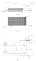
- FIG. 1A is a block diagram showing an exemplary fingerprint sensor device 1.
- the fingerprint sensor device 1 includes a sensor chip 2 disposed over a substrate carrier 4 and a protective film or cover layer 6 disposed over the sensor chip 2.
- the protective film or cover layer 6 includes an insulator or dielectric material such as glass, silicon dioxide (SiO 2 ), sapphire, plastic, polymer, other substantially similar materials.
- the protective film or cover layer 6 is configured to protect the sensor chip 2 and potentially function as a part of a dielectric layer between a surface of a finger 8 and conductive sensing electrodes of individual sensor pixels in the sensor chip 2.
- the protective film or cover layer 6 is an optional layer depending on the application of the fingerprint sensor device 1.
- the fingerprint sensor device 1 can be disposed through an opening of a top cover glass of an electronic device such as a mobile phone or under a top cover glass of the electronic device.
- the protective film or cover 6 is not needed because the top cover glass of the electronic device will function to protect the sensor chip 2 and act as the dielectric layer.
- the sensor chip 2 includes an array of sensor pixels that in combination senses or captures fingerprint data from the finger 8 in contact with the protective film or cover layer 6.
- Each sensor pixel of the sensor chip 2 generates an output signal (e.g., a voltage) based on a capacitance of a capacitor associated with a ridge or valley of the finger 8.
- the output signals when combined represents a fingerprint image of the finger 8. Higher the number of pixel sensors, greater the resolution of the fingerprint image.
- FIG. 1B is a diagram showing an exemplary sensor chip 2.
- the sensor chip 2 includes a pixelated sensor array 3 which occupies a significant portion of the sensor chip 2.
- Each sensor pixel in the pixelated sensing element array 3 includes a CMOS capacitive sensor or other types of sensors that can sense fingerprint features.
- the sensor chip 2 includes a signal processing unit 5 for processing signals received from all of the sensor pixels in the pixelated sensor array 3, and a connection unit 7 electrically coupled to the signal processing unit 5.
- the signal processing unit 5 includes various signal processing components including amplifiers, filters, and an analog to digital converter (ADC).
- the connection unit 7 includes multiple electrodes which can be connected to external circuitry through wire-bonding, bump bonding or other connection means.
- the connection unit 7 can be disposed along an edge of the sensor chip 2 for the convenience of interfacing with other components of the fingerprint sensor device 1.
- the array 3 of sensor pixels in the sensor chip 2 can be arranged to have various shapes and sizes.
- the array 3 of sensor pixels may be arranged to have a rectangular shape with a width of the rectangular shape being larger than a height of the rectangular shape.
- Exemplary sizes for the rectangular shaped sensor chip include 24 ⁇ 88, 32 ⁇ 88, 56 ⁇ 88 sensor pixels.
- the array 3 of sensor pixels in the sensor chip 2 may be arranged to have a square shape.
- Exemplary sizes for the square shaped sensor chip 2 include 32 ⁇ 32, 64 ⁇ 64, 96 ⁇ 96 and 128 ⁇ 128 sensor pixels.
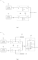
- FIG. 2 is a schematic diagram of an exemplary sensor pixel circuitry 10 according to an embodiment of the disclosed technology.
- the sensor pixel circuitry 10 corresponds to at least part of the structure within each sensor pixel in the array 3 of sensor pixels.
- the sensor pixel circuitry 10 includes a capacitive sensing layer 100, a layout layer 106, voltage generators 102 and 104, and switching circuitry such as switching networks 108 and 110.
- the circuitry of switching networks 108 and 110 can be implemented using sample-and-hold circuitry.
- the capacitive sensing layer 100 can be a conductive layer or electrode layer and can be implemented as one of the opposing sensor plates or electrodes in a capacitor.
- the capacitive sensing layer 100 and the surface of the finger form the two opposing plates of a capacitor.
- the capacitive sensing layer 100 includes a metal layer within an integrated circuitry (IC) layout, which forms a capacitor C1 with a ground terminal.
- IC integrated circuitry
- a passivation layer (not illustrated in FIG. 1 ) is usually disposed to cover the capacitive sensing layer 100, for receiving a touch of a user.
- the passivation layer may be the protective film or cover layer 6 shown in FIG 1A .
- the passivation layer is a top cover glass of an electronic device that function to protect the sensor chip 2 and act as the dielectric layer.
- the passivation layer includes insulating materials such as a glass, a sapphire, a plastic or a polymer, etc.
- the layout layer 106 may be a poly layer of conductive (e.g., metal) layers utilized for IC layout.
- the layout layer 106 forms a capacitor Cp2 with a signal ground terminal.
- the signal ground terminal is not limited to a system ground terminal with 0 voltage.
- a terminal or a layout layer receiving a fixed voltage is considered as a signal ground terminal.
- the capacitor Cp2 may be a parasitic capacitor between the layout layer 106 and another layout layer, or include a capacitor coupled between the layout layer 106 and the signal ground terminal.
- the voltage generators 102 and 104 are configured to generate drive voltages V1 and V2.
- the switching network 108 includes switches S1 and S2.
- the switches S1 and S2 are connected in series, and the capacitive sensing layer 100 is electrically coupled between the switches S1 and S2.
- the switching network 110 includes switches S3 and S4.
- the switches S3 and S4 are connected in series, and the layout layer 106 is electrically coupled between the switches S3 and S4.
- the switches S1 and S2 can be controlled by a clock signal or other control signals, such that the switching network 108 turns on an electrical connection between the voltage generator 102 and the capacitive sensing layer 100 by switching on the switch S1 and turns off an electrical connection between the capacitive sensing layer 100 and the output terminal N by switching off the switch S2 during a first period.
- the switching network 108 turns off the electrical connection between the voltage generator 102 and the capacitive sensing layer 100 by switching off the switch S1 and turns on the electrical connection between the capacitive sensing layer 100 and the output terminal N by switching on the switch S2.
- switch S1 operates as a charging switch
- switch S2 operates as a charge sensing switch to synchronously charge and sense capacitor C1 associated with the capacitive sensing layer 100 during respective time periods.
- the switches S3 and S4 can be controlled by a clock signal or other control signals, such that the switching network 110 turns on an electrical connection between the voltage generator 104 and the layout layer 106 by switching on switch S3 and turns off an electrical connection between the layout layer 106 and the output terminal N by switching off switch S4 during the first period.
- the switching network 110 turns off the electrical connection between the voltage generator 104 and the layout layer 106 by switching off switch S3 and turns on the electrical connection between the layout layer 106 and the output terminal N by switching on switch S4.
- switch S3 operates as a charging switch
- switch S4 operates as a charge sensing switch to synchronously charge and sense capacitor Cp2 associated with the integrated circuit layout layer 106 during respective time periods.
- the switching networks 108 and 110 can adequately charge the capacitors C1 and Cp2 using the voltage generators 102 and 104, and output the charging result through the output terminal N to enhance an accuracy of fingerprint identification.
- the voltage generators 102 and 104 can vary the voltages generated V1 and V2 to enhance the accuracy of fingerprint identification.
- the capacitor C1 formed between the capacitive sensing layer 100 and the ground terminal includes a parasitic capacitor Cp1 formed between the capacitive sensing layer 100 and the ground terminal, and a touch sensing capacitor Cf formed when the user's finger (e.g., a ridge of the finger) is touching the passivation layer over the capacitive sensing layer 100.
- the capacitance value of the touch sensing capacitor Cf is substantially 0, and when the user's finger touches the passivation layer over the capacitive sensing layer 100, the touching capacitor Cf has a nonzero capacitance value that depends on the spacing from the capacitive sensing layer 100. Therefore, the capacitance value of the capacitor C1 varies according to whether the user's finger touches the passivation layer over the capacitive sensing layer 100 and the local spacing between a location on the touched part of the finger and the layer 100.
- the capacitance value of the touch sensing capacitor Cf varies from one part of the finger to another part according to a distance between the portion of the finger (e.g., a ridge of the finger) touching the passivation layer over the capacitive sensing layer 100 and the capacitive sensing layer 100.
- This variation in the touch sensing capacitor Cf is captured by the array of sensor pixels and the output of the array of sensor pixels provides a map representing the surface profile of the touched portion of the finger and thus can be used to reconstruct the fingerprint pattern.
- This reconstruction based on the spatial variation in the touch sensing capacitor Cf can be achieved by the subsequent signal processing circuitry.
- a fingerprint identification system that implements structures and functions substantially equivalent to the sensor chip 2 in FIG. 1B includes a signal processing unit (e.g., substantially similar to the signal processing unit 5 of the sensor chip 2) in communication with the sensor pixel circuitry (e.g., substantially similar to the array 3 of sensor pixels) can sense the capacitance variation of the touch sensing capacitor Cf, and determine a location of the capacitive sensing layer 100 corresponds to a ridge or valley of the finger touching the passivation layer over the capacitive sensing layer 100.
- a signal processing unit e.g., substantially similar to the signal processing unit 5 of the sensor chip 2
- the sensor pixel circuitry e.g., substantially similar to the array 3 of sensor pixels
- FIG. 3 is a circuit diagram showing an exemplary circuit equivalent of the sensor pixel circuitry 10.
- the switches S1 through S4 are controlled by a clock signal to control the on-off states of the switches.
- the switches S2 and S4 are turned off when the switches S1 and S3 are turned on, and the switches S2 and S4 are turned on when the switches S1 and S3 are turned off.
- voltage V1 charges capacitor C1
- voltage V2 charges capacitor Cp2.
- the capacitor C1 exchanges electric charges with capacitor Cp2 to form a resulting voltage Vr at the output terminal N.
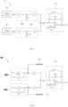
- FIG. 4 is a schematic diagram of an exemplary sensor pixel circuitry 30 according to an embodiment of the disclosed technology.
- FIG. 5 is a schematic diagram of an equivalent circuitry of the sensor pixel circuitry 30.
- the sensor pixel circuitry 30 is substantially similar to the sensor pixel circuitry 10. Different from the sensor pixel circuitry 10, the sensor pixel circuitry 30 includes an integrator INT electrically coupled to the output terminal N, for storing the electric charges V1*Cf caused by ridges and valleys touching the passivation layer over the capacitance sensing layer100.
- the inclusion of the integrator INT enhances the signal-to-noise ratio (SNR).
- the integrator INT includes a reference voltage generator 300, an amplifier OP, an integrating capacitor Cint and a reset switch Srst.
- the reference voltage generator 300 is configured to generate a reference voltage Vref.
- the amplifier OP includes a positive input terminal electrically coupled to the reference voltage generator 300 for receiving the reference voltage Vref, a negative input terminal electrically coupled to the output terminal N for receiving the resulting voltage Vr, and an output terminal for outputting an output voltage Vo.
- the integrating capacitor Cint and the reset switch Srst are electrically coupled between the negative input terminal of the amplifier OP and the output terminal.
- a capacitance value of the parasitic capacitor Cp1 within the capacitor C1 is usually larger than a capacitance value of the touch sensing capacitor Cf, which makes it difficult to identify a variation in the capacitance of the touch sensing capacitor Cf.
- the voltage value of the reference voltage Vref received by the negative input terminal of the amplifier OP in the sensor pixel circuitry 30 can be adjusted, such that the capacitance variation of the touch sensing capacitor Cf is more prominently identified through the integrator.
- the total electric charges accumulated by the capacitor C1 and the capacitor Cp2 during the first period are larger than Vref * ( Cp1+ Cp2), and there are electric charges to be stored in the integrating capacitor Cint.
- the output voltage Vo reflects the capacitance value of the touch sensing capacitor Cf more prominently.
- the reference voltage Vref can reduce or even eliminate the effect of the parasitic capacitor Cp1 on the determination of the capacitance value of the touch sensing capacitor Cf.
- the capacitance values of the capacitors Cp1 and Cp2 may not be easily acquired.
- V1 generated by the voltage generator 102 the capacitance mismatch of the capacitors Cp1 and Cp2 due to fabrication process can be substantially eliminated.
- the capacitors Cp1 and Cp2 can be designed to have substantially equal capacitance value
- the voltage values of the voltages V1 and V2 can be adjusted to substantially eliminate the capacitance mismatch of the capacitors Cp1 and Cp2 due to fabrication.
- the sensor pixel circuitry of the disclosed technology can enhance the accuracy of fingerprint identification.
- Various modifications can be made to the above described sensor pixel circuitry (e.g., array of sensor pixels 3) and fingerprint identification system (e.g., sensor chip 2 that includes an array of sensor pixels 3 and a signal processing system 5).
- fingerprint identification system e.g., sensor chip 2 that includes an array of sensor pixels 3 and a signal processing system 5.
- DAC digital to analog converter
- the voltage generator 102 includes a DAC, which is controlled to output the voltage V1 with a variable voltage value.
- the voltage generator 104 includes a DAC, which is controlled to output the voltage V2 with a variable voltage value.
- the reference voltage generator 300 includes a DAC, which is controlled to output the reference voltage Vref with a variable voltage value.
- FIG. 6 is a schematic diagram of an exemplary sensor pixel circuitry 60 according to an embodiment of the disclosed technology.
- the sensor pixel circuitry 60 can be substantially similar to the sensor pixel circuitry 30.
- the sensor pixel circuitry 60 utilizes electric charge supplying modules 602 and 604 to function as the voltage generators 102 and 104 of the sensor pixel circuitry 30 in FIGS. 2 , 3 4 and 5 .
- the electric charge supplying module 602 is electrically coupled between the switch S2 and the capacitive sensing layer 100.
- the electric charge supplying module 604 is electrically coupled between the switch S4 and the layout layer 106.
- the electric charge supplying module 602 includes the switches S11 and S12 electrically coupled to a voltage V+ and a voltage V - , respectively.
- the electric charge supplying module 604 includes the switches S31 and S32 electrically coupled to a voltage V+ and a voltage V - , respectively.
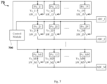
- FIGS. 7 through 8 illustrate exemplary embodiments of a fingerprint identification system using an exemplary sensor pixel array arrangement to detect a presence of a ridge or valley of a finger at a specific location of the single sensor pixel circuitry.
- Proper arrangement of the sensor pixel circuitry in a fingerprint identification system can assist in identification of a user's fingerprint.
- FIG. 7 is a schematic diagram of an exemplary fingerprint identification system 70.
- the fingerprint identification system 70 is an implementation of the sensor chip 2 that combines the structures and functions of the array 3 of sensor pixels in electrical communication with the signal processing system 5 as shown in FIG 1B .
- the fingerprint identification system includes an array of sensor pixel circuitry Pix_11 through Pix_MN, corresponding enable switches SW_11 through SW_MN, corresponding analog to digital converters ADC_1 through ADC_M and a control module 700.
- the sensor pixel circuitry Pix_11 through Pix_MN are arranged in an exemplary array configuration.
- the array of sensor pixel circuitry Pix_11 through Pix_MN are arranged in M rows and N columns.
- Each sensor pixel circuitry corresponds to and electrically coupled to an enable switch, and a row of sensor pixel circuitry correspond to and electrically coupled to an analog to digital converter.
- the group (e.g., row or column) of sensor pixel circuitry Pix_11 through Pix_1N are electrically coupled to the analog to a corresponding digital converter ADC_1.
- the group of sensor pixel circuitry Pix_21 through Pix_2N are electrically coupled to the analog to digital converter ADC_2.
- Remaining groups of sensor pixel circuitry can be similarly electrically coupled to corresponding analog to digital converters.
- the array of sensor pixel circuitry Pix_11 through Pix_MN and the enable switches SW_11 through SW_MN are electrically coupled to the control module 700 for receiving control signals generated by the control module 700.
- Each sensor pixel circuitry of the array of sensor pixel circuitry Pix_11 through Pix_MN can be substantially similar to the sensor pixel circuitry 30 or 60 or any other configurations described in this patent document.
- output voltages Vo_11 through Vo_MN are outputted by the integrators of the sensor pixel circuitry Pix_11 through Pix_MN.
- multiple sensor pixel circuitry can share one integrator for various potential advantages including to save layout space and to simplify the design, for example.
- the operational principles and detail operations of each sensor pixel circuitry in the array of sensor pixel circuitry Pix_11 through Pix_MN can be substantially similar to the description of the sensor pixel circuitry 30 or 60 or any other configurations described in this patent document.
- the control module 700 controls the enable switches SW_11 through SW_MN, such that a conducting period of an enable switch corresponding to a given sensor pixel circuitry in the array of sensor pixel circuitry (e.g., Pix_11 through Pix_MN) and a conducting period of an enable switch corresponding to another sensor pixel circuitry of the same row of sensor pixel circuitry (e.g., Pix_11 through Pix_MN) can differ in time.
- the control module 700 selectively turns on and off the switches SW_11 through SW_MN to selectively vary the conducting period of the different sensor pixel circuitry in the same row (e.g., Pix_11 through Pix_MN) for readout by ADC.
- the control module 700 is configured to control the sensor pixel circuitry for the other rows in a similar manner.
- the control module 700 is configured to turn on the enable switches of the array of sensor pixel circuitry substantially in parallel.
- the control module 700 can enable SW11 through SWMN at substantially the same time, so that ADC 1-M are configured to readout data in parallel.
- the control module 700 is configured to scan through one or more lines (e.g., rows, columns, or other groups) at a time to readout all of the pixel output voltage.
- FIG. 8 illustrates examples of waveforms of various signals associated with a fingerprint identification system.
- the example waves shown in FIG. 8 are associated with row M of the rows of sensor pixel circuitry in FIG. 7 .
- An output of an integrator (e.g., integrator INT) is represented by the output voltage Vo_m1.
- the control signal of the enable switch SW_m1 pulls high at a time t1 for a time period, and the output voltage Vo_m1 is delivered to the analog to digital converter ADC_m through the enable switch SW_m1.
- the control signal of the reset switch Srst pulls high at a time tr1, such that the integrating capacitor Cint of the sensor pixel circuitry Pix_m1 is return to zero, so as to be ready for performing another integration for a next time period.
- the integrator of the sensor pixel circuitry Pix_m2 also performs integration substantially simultaneously.
- the control signal of the enable switch SW_m2 pulls high at a time t2 for a time period, and the output voltage Vo_m2 is delivered to the analog to digital converter ADC_m through the enable switch SW_m2.
- the time t2 is at some time after t1.
- each of the sensor pixel circuitry Pix_m3 through Pix_mN is configured to deliver the output voltages to the corresponding analog to digital converter ADC_m at different after time t2.
- the different time instances for sensor pixel circuitry Pix_m1 through Pix_mN may be non-overlapping time instances.
- the analog to digital converter ADC_m receives the output voltage of each sensor pixel circuitry in the row of the sensor pixel circuitry Pix_m1 through Pix_mN.
- Each sensor pixel circuitry within the array of sensor pixel circuitry Pix_11 through Pix_MN includes a dedicated integrator. As such, the integration processes of the different sensor pixel circuitry in a given row of sensor pixel circuitry (e.g., Pix_m1 through Pix_mN) can be performed in parallel by the multiple integrators. With a fixed integration period for each integrator, the fingerprint identification system 70 can shorten an overall integration period for the array of sensor pixel circuitry.
- the overall integration period for a row of sensor pixel circuitry can be fixed (e.g., at a period longer than individual sensor pixel circuitry integration period) to allow a longer integration period for each sensor pixel circuitry in the rows of sensor pixel circuitry Pix_m1 through Pix_mn. Because the individual integration processes can be performed in parallel for all pixel sensor circuitry, the overall integration period can be reduced even when the individual integration period is increased. Increasing the individual integration period, while reducing the overall integration period, can allow the noise to be sufficiently averaged, and the SNR of the sensor pixel circuitry can be further enhanced. Because each pixel integrator can act as a pixel level signal (voltage) storage, and the stored signal can be readout later by a scan readout process using the ADCs and control module, for example.
- a selected subset or the entire array of sensor pixel circuitry can be enabled to integrate the selected subset or the entire array of sensor pixel circuitry.
- the integrating capacitor connected to the negative feedback path of each integrator can be used as a local memory to store the charges associated with the corresponding sensor pixel. Readout of the sensor pixel data can be performed per selected group or subset of the array of senor pixel circuitry, such as each row, column, etc.
- Readout process is a relatively quick compared to the integration process, and thus, parallel integration of the selected subset or the entire array of sensor pixel circuitry while the finger is touching the fingerprint identification system (e.g., the passivation layer over the sensor pixel circuitry) can be advantageous by not wasting the sensor pixel circuitry under the finger touch.
- the fingerprint identification system e.g., the passivation layer over the sensor pixel circuitry
- the fingerprint identification system can apply an excitation signal directly to a finger via an electrode to increase a voltage difference between two terminals of the touch sensing capacitor Cf, such that more electric charges are accumulated in the touch sensing capacitor Cf during the first period.
- the fingerprint identification system can apply a high voltage to the finger during the second period, such that more electric charges are stored in the integrating capacitor Cint.
- FIG. 9 is a schematic diagram of an exemplary sensor pixel circuitry 90 and an external electrode Et.
- the sensor pixel circuitry 90 can be substantially similar to the sensor pixel circuitry 30 or 60.
- the switches S1 and S3 are controlled by the clock signal ck1, and the switches S2 and S4 are controlled by the clock signal ck2.
- the clock signal ck1 is high, the switches S1 and S3 are turned on.
- the clock signal ck1 is low, the switches S1 and S3 are turned off.
- the clock signal ck2 is high, the switches S2 and S4 are turned on.
- the switches S2 and S4 are turned off
- the external electrode Et can be electrically connected to the clock signal ck2, so as to pull high the voltage applied to the user's finger through the external electrode Et during the second period (i.e., the period when the switches S2 and S4 are turned on and the switches S1 and S3 are turned off).
- the second period i.e., the period when the switches S2 and S4 are turned on and the switches S1 and S3 are turned off.
- FIG. 10 is a schematic diagram illustrating exemplary waveforms of clock signals ck1 and ck2.
- the clock signals ck1 and ck2 are inverted and out of phase with each other.
- ck1 is set high
- ck2 is set low.
- a row of sensor pixel circuitry (e.g., Pix_m1 through Pix_mN) are couple to a corresponding analog to digital converter (e.g., ADC_m).
- the sensor pixel circuitry units can be divided into different groups of sensor pixel circuitry. All sensor pixel circuitry in a given group can be electrically coupled to the same corresponding analog to digital converter.
- the groups of sensor pixel circuitry can be determined using rows, columns, a predetermined number of sensor pixel circuitry, a particular shape (e.g., a square) or other groupings that allow an enable switch corresponding to a sensor pixel circuitry in one group to have a different conducting period than another enable switch corresponding to a sensor pixel circuitry in a different group.
- a particular shape e.g., a square
- FIGS. 11, 12 and 13 Additional examples of modifications to the sensor pixel circuitry are shown FIGS. 11, 12 and 13 .
- FIG. 11 is a diagram showing another exemplary sensor pixel circuitry 1100 for compensating for capacitor mismatch in a fingerprint identification system.
- the exemplary sensor pixel circuitry includes a sensor plate or a capacitive sensing layer 1102 configured to operate or function as one of two opposing conductive plates of a fingerprint associated capacitor. For example, when a finger 1108 of a user approaches the sensor plate or capacitive sensing layer 1102, a surface of the finger 1108 and the sensor plate of capacitive sensing layer 1102 configured to operate or function as the two opposing plates of capacitor Cf.
- the capacitance of the capacitor Cf can vary based at least partly on a distance between the surface of the finger (e.g., a ridge) and the sensor plate or capacitive sensing layer 1102.
- the sensor plate or capacitive sensing layer 1102 includes a conductive material, such as one of various metals.
- a voltage generator 1132 is electrically connected to the sensor plate 1102, which is electrically connected to a system ground through the surface of the finger 108. The voltage generator is configured to generate drive voltage VDD for charging the fingerprint associated capacitor Cf.
- a switching circuitry, such as a switching network 1120 includes switches 1122 and 1124 in series for being switchable in electrically connecting the sensor plate 1102 to the voltage generator 1132 and an output terminal 1140. In some implementations, the switching circuitry 1120 can be implemented using sample-and-hold circuitry.
- the switches 1122 and 1124 can be controlled by a clock signal or other control signals, such that the switching circuitry 1120 is configured to turn on an electrical connection between the voltage generator 1132 and the sensor plate 1102 by turning on the switch 1122 and turn off an electrical connection between the sensor plate 1102 and the output terminal 1140 by turning off the switch 1124 during a first period.
- the sample-and-hold circuitry 1120 is configured to turn off the electrical connection between the voltage generator 1132 and the sensor plate 1102 by turning off the switch 1122 and turn on the electrical connection between the sensor plate 1102 and the output terminal 1140 by turning on the switch 1124.
- switch 1122 operates as a charging switch
- switch 1124 operates as a charge sensing switch to synchronously charge and sense capacitor Cf associated with the sensor plate 1102 during respective time periods.
- Two substantially identical conductive layers, electrodes or plates 1104 and 1106 can be disposed below the sensor plate 1102.
- the conductive plate 1104 and the sensor plate 1102 form a corresponding capacitor CP1.
- the conductive plate 1106 and the sensor plate 1102 form a corresponding capacitor CP2.
- a switching circuitry such as a switching network 1126 includes switches 1128 and 1130 to switchable between electrically connecting the conductive plate 1104 to a voltage generator 1134 and ground 1144.
- the other conductive plate 1106 is electrically connected to ground and not electrically controlled by the switching circuitry 1126.
- the voltage generator 1134 includes a DAC1 1136 and a voltage buffer 1138 to generate and provide a variable voltage to the conductive plates 1104.
- the switching circuitry 1126 can be implemented using sample-and-hold circuitry.
- the switches 1128 and 1130 can be controlled by a clock signal or other control signals, such that the switching circuitry 1126 is configured to turn on an electrical connection between the voltage generator 1134 and the conductive plate 1104 by turning on the switch 1128 and turn off an electrical connection between the conductive plate 1104 and the ground 1144 by turning off the switch 1130 during a first period. During a second period, the switching circuitry 1126 is configured to turn off the electrical connection between the voltage generator 1134 and the conductive plate 1104 by turning off the switch 1128 and turn on the electrical connection between the conductive plate 1104 and the ground 1144 by turning on the switch 1130.
- switch 1128 operates as a charging switch
- switch 1130 operates as a grounding switch to synchronously charge and ground capacitor CP1 associated with the sensor plate 1102 during respective time periods.
- the output terminal 1140 is configured to be optionally electrically connected to an integrator 1142 for storing the electric charges caused by ridges and valleys of a finger touching the passivation layer over the sensor plate 1102.
- the inclusion of the integrator INT enhances the signal-to-noise ratio (SNR).
- the integrator includes an amplifier 1118 having a negative input electrically connected to the output terminal 1140 connected to the switching circuitry 1120.
- the amplifier 1118 has a positive input electrically connected to a reference voltage generator 1112 for receiving the reference voltage Vref.
- the reference voltage generator 1112 includes a DAC2 1114 and a voltage buffer 1116 for generating and providing a variable reference voltage.
- the amplifier 1118 includes an output terminal 114 for outputting an output voltage Vpo.
- An integrating capacitor Cint 1146 and a reset switch rst 1148 are electrically coupled in parallel between the negative input terminal of the amplifier OP 1118 and the output terminal 1144.
- the DAC1 1136 output can be set to VDD.
- the switches 1122 and 1128 are turned on and switches 1124 and 1130 are turned off.
- the charge in CP2 will be Cp2*VDD and the charge in CP1 will be 0.
- switches 1122 and 1128 are turned off and switches 1124 and 1130 are turned on.
- the charges in CP1 and CP2 will exchange.
- the charge in Cf is substantially zero, and the voltage at the negative input of the amplifier OP 1118 will be VDD/2.
- the DAC1 might be not necessary or become optional. By removing the DAC1, the DAC1 noise will no longer exist in the pixel output, which further enhances the SNR.
- FIG. 12 is a diagram showing yet another exemplary sensor pixel circuitry 1200 for compensating for capacitor mismatch in a fingerprint identification system.
- the sensor pixel circuitry 1200 is substantially similar to the sensor pixel circuitry 1100 with some variations.
- the switching circuitry 1126 is electrically connected between the conductive plate 1104 and a voltage generator 1202 that does not include a DAC.
- the output of the voltage generator 1202 preset to VDD.
- a third voltage generator 1212 is electrically connected to another switching circuitry 1204.
- the third voltage generator 1212 includes a DAC 1214 DAC1 in series with a voltage buffer 1216.
- the switching circuitry 1204 includes switches 1206 and 1208 in series for being switchable in electrically connecting a capacitor 1210 Cc between the voltage generator 1212 and a common node 1218 connecting to the sensor plate 1102 and the switching circuitry 1120 (which is switchable in electrically connecting to the output terminal 1140 and the voltage generator 1132).
- the other terminal of the capacitor 1210 Cc is electrically connected to ground. See relevant description of FIG. 11 for the circuit components of the sensor pixel circuitry 1200 that are similar to the sensor pixel circuitry 1100.
- the final voltage VPO at the output terminal 1144 without a finger touching a passivation layer over the sensor electrode 1102 during the second period is (CP1*VDD+Cc*VDAC)/(Cc+Cp1+Cp2).
- VDAC is set to VDD/2.
- VDAC is adjusted.
- FIG. 13 is a diagram showing yet another exemplary sensor pixel circuitry 1300 for compensating for capacitor mismatch in a fingerprint identification system.
- the sensor pixel circuitry 1300 is substantially similar to the sensor pixel circuitry 1200 with some variations.
- the switching circuitry 1204 includes switches 1206 and 1208 electrically connected in series for selectively electrically connecting the capacitor Cc 1210 to the voltage generator 1202 and a fourth voltage generator 1220.
- the voltage generator 1220 can be set to VDD.
- the other terminal of the capacitor Cc 1210 is electrically connected to a common node 1218 connecting to the sensor plate 1102 and the sample-and-hold circuitry 1120 (which is switchable in electrically connecting to the output terminal 1140 and the voltage generator 1132). See descriptions of FIG. 12 for the corresponding descriptions of the circuit components of the sensor pixel circuitry 1300 that are similar to the sensor pixel circuitry 1200.
- the final voltage VPO at output terminal 1144 without a finger touch during the second period Ck2 is (CP1*VDD+Cc*Vdac)/(Cc+Cp1+Cp2).
- VDAC is adjusted.
- an integrator can be shared between a number of sensor pixel circuitry units to reduce the total number of integrators in the fingerprint identification system, which provides a number potential advantages including cost reduction, layout size reduction, and simplicity in design, for example.
- Multiple units of sensor pixel circuitry share an integrator by multiplexing the output signals from a selected number of sensor pixel circuitry units into a shared integrator. For example, when grouping the array of sensor pixel circuitry units into rows, with each row assigned to an ADC, each sensor pixel circuitry unit in a row share an integrator with one or more sensor pixel circuitry units in one or more rows of sensor pixel circuitry. When grouping the sensor pixel circuitry in the array of sensor pixel circuitry into columns, each sensor pixel circuitry in a given column share an integrator with one or more sensor pixel circuitry in one or more columns.
- FIGS. 14A and 14B show examples of configurations for sharing integrators between sensor pixel circuitry units.
- FIG 14A is a diagram showing an example of a fingerprint identification system 1400 for integrator sharing between rows in an array of sensor pixel circuitry units.
- the fingerprint identification system 1400 includes a control module 1402, which is substantially similar to the control module 700 in FIG. 7 .
- An array of sensor pixel circuitry Sensor Pixel 11 through Sensor Pixel MN are grouped into rows 1 through M. Each row in the array includes N columns of sensor pixel circuitry. In the example shown in FIG. 14A , every two rows of sensor pixel circuitry share integrators. However, more than two rows of sensor pixel circuitry share integrators.
- the control module 1402 is configured to selectively enable/disable each sensor pixel circuitry in the array by turning on and off corresponding enable switches SW11 through SW MN.
- the switch signal may be one or multiple digital logic signals.
- the control module 1402 is configured to integrate any number of sensor pixel circuitry in the array in parallel.
- the control module enables the odd row of sensor pixel circuitry (e.g., Sensor Pixel 11 through Sensor Pixel 1N) to integrate all sensor pixels in the row.
- the pixels in the odd row are configured to perform integration in parallel, and after the integration is completed, control module scans each pixels to readout their data using the ADCs.
- control module switch on the even row of sensor pixel circuitry (e.g., Sensor Pixel 21 through Sensor Pixel 2N), which shares the integrators used by the odd row of sensor pixel circuitry (e.g., Sensor Pixel 11 through Sensor Pixel 1N) to perform integration in parallel.
- All of the odd and even rows can be processed in similar manner. In some implementations, all odd rows can be processed at substantially the same time in parallel. Then all of the even rows can be processed at substantially the same time in parallel. In some implementations, any number of odd and even rows can be processed together in parallel. In addition, the even rows can be processed first in some implementations. Thus, the order of the even and odd rows is not limiting.
- FIG 14B is a diagram showing an exemplary fingerprint identification system 1410 for integrator sharing between columns in an array of sensor pixel circuitry.
- the fingerprint identification system 1410 includes a control module 1402, which can be substantially similar to the control module 700 in FIG. 7 .
- An array of sensor pixel circuitry Sensor Pixel 11 through Sensor Pixel 4N are grouped into columns 1 through 4. While more than 4 columns is included in an array, only 4 columns are shown in FIG. 14B for illustrative purposes.
- Each column in the array includes N rows of sensor pixel circuitry. In the example shown in FIG. 14B , every two columns of sensor pixel circuitry share integrators. However, more than two columns of sensor pixel circuitry share integrators.
- the control module 1402 is configured to selectively enable/disable each sensor pixel circuitry in the array by turning on and off corresponding enable switches SW11 through SW 4N. By controlling the appropriate sensor pixel circuitry through the enable switches, the control module 1402 is configured to integrate any number of sensor pixel circuitry in the array in parallel. In the example shown in FIG. 14B , the control module enables the odd column of sensor pixel circuitry (e.g., Sensor Pixel 11 through Sensor Pixel 1N) to integrate all sensor pixels in the odd column. The sensor pixels in the odd column are configured to perform integration in parallel, and after the integration completed, control module is configured to scan each sensor pixel to readout the data using the ADCs.
- the control module enables the odd column of sensor pixel circuitry (e.g., Sensor Pixel 11 through Sensor Pixel 1N) to integrate all sensor pixels in the odd column.
- the sensor pixels in the odd column are configured to perform integration in parallel, and after the integration completed, control module is configured to scan each sensor pixel to readout the data using the ADCs.
- the control module is configured to switch on the even column of sensor pixel circuitry (e.g., Sensor Pixel 21 through Sensor Pixel 2N), which shares the integrators used by the odd column of sensor pixel circuitry (e.g., Sensor Pixel 11 through Sensor Pixel 1N) to perform integration in parallel.
- All of the odd and even columns can be processed in similar manner. In some implementations, all odd columns can be processed at substantially the same time in parallel. Then all of the even columns can be processed at substantially the same time in parallel. In some implementations, any number of odd and even columns can be processed together in parallel. In addition, the even columns can be processed first in some implementations. Thus, the order of the even and odd columns is not limiting.
- the array of sensor pixels can be grouped in a way different than rows or columns and the integrator sharing can be implemented in various ways depending on the grouping of the array of sensor pixels.
- FIG. 14C is a diagram showing an exemplary sensor pixel circuitry and fingerprint identification system 1420 with two sensor pixel circuitry sharing an integrator.
- the fingerprint identification system 1420 shows a simple example where two sensor pixel circuitry 1422 and 1424 share one integrator 1426.
- the sensor pixel circuitry 1422 and 1424 can be substantially similar to sensor pixel circuitry 10 in FIG. 2 or any other configurations described in this patent document.
- FIG. 14D is a diagram showing an exemplary sensor pixel circuitry and fingerprint identification system 1430 with two sensor pixel circuitry sharing an integrator.
- the fingerprint identification system 1430 shows a simple example where two sensor pixel circuitry 1432 and 1434 share one integrator 1436.
- the sensor pixel circuitry 1422 and 1424 can be substantially similar to sensor pixel circuitry in FIGS. 11, 12 and 13 or any other configurations described in this patent document.
- FIGS. 14A , 14B , 14C and 14D some of the components including the ADC are not included in the figures for illustrative purposes only.
- the disclosed technology utilizes integrators for storing the electric charges accumulated by the touch sensing capacitor, utilizes the voltage generator for outputting the variable voltage and adjusting the electric charges stored in the parasitic capacitors, and utilizes the sensor pixel circuitry with a dedicated integrator for performing integration across a group of sensor pixel circuitry in parallel to enhance the SNR.
- the sensor pixel circuitry and the fingerprint identification system described in this patent document provide accurate fingerprint identification even without a metal ring.
Landscapes
- Engineering & Computer Science (AREA)
- Human Computer Interaction (AREA)
- Physics & Mathematics (AREA)
- General Physics & Mathematics (AREA)
- Multimedia (AREA)
- Theoretical Computer Science (AREA)
- Image Input (AREA)
- Measurement Of The Respiration, Hearing Ability, Form, And Blood Characteristics Of Living Organisms (AREA)
- Measurement Of Length, Angles, Or The Like Using Electric Or Magnetic Means (AREA)
Claims (10)
- Dispositif capteur d'empreintes digitales pour la détection d'empreintes digitales, comprenant :
un réseau (3) de pixels capteurs configuré pour se coupler de façon capacitive avec une portion tactile d'un doigt (8) pour former un réseau de condensateurs associés à l'empreinte digitale ayant des valeurs capacitives indicatives d'une empreinte digitale, chaque pixel capteur comportant :une borne de sortie (Vr) configurée pour émettre un signal de sortie qui indique un couplage capacitif local avec la portion touchée du doigt (8) en tant que partie de données d'empreintes digitales pour la détection d'empreintes digitales ;une couche de détection capacitive (100) comportant un matériau électriquement conducteur qui peut se coupler de façon capacitive à une partie locale de la portion tactile du doigt (8) formant un condensateur associé à l'empreinte digitale ;une couche de configuration de circuit intégré (106) qui est électriquement conductrice et couplée de façon capacitive à une borne de masse, formant un condensateur associé à la configuration ;un générateur de tension d'empreinte digitale (102) couplé électriquement pour alimenter en puissance la couche de détection capacitive (100) pour générer une tension d'empreinte digitale pour charger le condensateur associé à l'empreinte digitale ;un générateur de tension de configuration (104) couplé électriquement pour alimenter en puissance la couche de configuration de circuit intégré (106) pour générer une tension de configuration pour charger le condensateur associé à la configuration ;un ensemble de circuits de commutation d'empreintes digitales (108) configuré pour commuter entre la connexion électrique de la couche de détection capacitive (100) au générateur de tension d'empreinte digitale (102) et la borne de sortie (Vr) pour charger sélectivement le condensateur associé à l'empreinte digitale à l'aide de la tension d'empreinte digitale ; etun ensemble de circuits de configuration (110) configuré pour commuter entre la connexion électrique de la couche de configuration de circuit intégré (106) au générateur de tension de configuration (104) et la borne de sortie (Vr) pour charger sélectivement le condensateur associé à la configuration à l'aide de la tension de configuration ;dans lequel la couche de détection capacitive (100) et la couche de configuration de circuit intégré (106) sont toutes deux couplées à la borne de sortie (Vr) pour former un signal de sortie lorsque la couche de détection capacitive (100) est connectée électriquement à la borne de sortie (Vr), et la couche de configuration de circuit intégré (106) est connectée électriquement à la borne de sortie (Vr). - Dispositif capteur d'empreintes digitales de la revendication 1, dans lequel l'ensemble de circuits de commutation d'empreintes digitales (108) comporte :un commutateur de charge (S1) connecté électriquement entre le générateur de tension d'empreinte digitale (102) et la couche de détection capacitive (106) pour charger sélectivement le condensateur associé à l'empreinte digitale pendant une période de charge ; etun commutateur de détection (S2) connecté électriquement entre la couche de détection capacitive (106) et la borne de sortie (Vr) pour détecter sélectivement un signal associé au condensateur associé à l'empreinte digitale chargé pendant une période de détection différente de la période de charge.
- Dispositif capteur d'empreintes digitales de la revendication 1, dans lequel l'ensemble de circuits de configuration (110) comporte :un commutateur de charge (S3) connecté électriquement entre le générateur de tension de configuration (104) et la couche de configuration de circuit intégré (106) pour charger sélectivement le condensateur associé à la configuration pendant une période de charge ; etun commutateur de détection (S4) connecté électriquement entre la couche de configuration de circuit intégré (106) et la borne de sortie (Vr) pour détecter sélectivement un signal associé au condensateur associé à la configuration chargé pendant une période de détection différente de la période de charge.
- Dispositif capteur d'empreintes digitales de la revendication 1, dans lequel la couche de détection capacitive (100) est configurée pour former avec la surface d'un doigt (8) deux électrodes conductrices opposées du condensateur associé au doigt.
- Dispositif capteur d'empreintes digitales de la revendication 1, dans lequel le générateur de tension d'empreinte digitale (102) et le générateur de tension de configuration (104) sont configurés pour faire varier les empreintes digitales et les tensions de configuration générées indépendamment l'une de l'autre.
- Dispositif capteur d'empreintes digitales de la revendication 1, comprenant :
un intégrateur (INT) couplé électriquement à la borne de sortie (Vr) connectée au condensateur associé à l'empreinte digitale et au condensateur associé à la configuration pour stocker des charges électriques associées au condensateur associé à l'empreinte digitale chargé en réponse à un toucher par un doigt (8) d'un utilisateur. - Dispositif capteur d'empreintes digitales de la revendication 6, dans lequel l'intégrateur (INT) comprend :un générateur de tension de référence (300) configuré pour générer une tension de référence ;un amplificateur (OP), comprenant :une borne d'entrée positive couplée électriquement au générateur de tension de référence (OP) pour recevoir la tension de référence ;une borne d'entrée négative couplée électriquement à la borne de sortie (Vr) connectée au condensateur associé à l'empreinte digitale et au condensateur associé à la configuration ; etune borne de sortie de l'amplificateur ;un condensateur d'intégration (Cint) couplé électriquement entre la borne d'entrée négative et la borne de sortie de l'amplificateur (OP) ; etun commutateur de réinitialisation (Srst) couplé électriquement entre la borne d'entrée négative et la borne de sortie de l'amplificateur (OP).
- Dispositif capteur d'empreintes digitales de la revendication 1, dans lequel la borne de sortie (Vr) connectée au condensateur associé à l'empreinte digitale et au condensateur associé à la configuration est configurée pour générer le signal de sortie associé à une crête ou à un creux d'un doigt (8).
- Dispositif capteur d'empreintes digitales de la revendication 1, dans lequelle réseau de pixels capteurs est agencé pour former des groupes d'ensembles de circuits de pixels capteurs (Pix_11∼Pix_MN) connectés électriquement fonctionnant pour capturer un motif d'empreintes digitales de la portion tactile du doigt (8) ;dans lequel le dispositif capteur d'empreintes digitales comprend un convertisseur analogique-numérique (ADC_1∼ADC_M) couplé électriquement à chaque groupe d'ensembles de circuits de pixels capteurs (Pix_11~Pix_MN) connectés électriquement ;dans lequel le dispositif capteur d'empreintes digitales comprend un module de commande (700) couplé électriquement à chaque ensemble de circuits de pixels capteurs (Pix_11∼Pix_MN) dans le réseau, le module de commande (700) étant configuré pour générer un signal de commande pour commander chaque ensemble de circuits de pixels capteurs (Pix_11∼Pix_MN) dans le réseau ;dans lequel chaque ensemble de circuits de pixels capteurs (Pix_11~Pix_MN) dans un groupe d'ensembles de circuits de pixels capteurs connectés électriquement comprend :
un commutateur de validation (SW_11~SW_MN) couplé électriquement entre chaque ensemble de circuits de pixels capteurs (Pix_11∼Pix_MN) et le convertisseur analogique-numérique (ADC_1~ADC_M) qui correspond au groupe d'ensembles de circuits de pixels capteurs (Pix_11∼Pix_MN) connectés électriquement. - Dispositif capteur d'empreintes digitales de la revendication 9, dans lequel :
le module de commande est configuré pour générer le signal de commande pour commander chaque ensemble de circuits de pixels capteurs dans le réseau pour intégrer le signal de sortie dans chaque ensemble de circuits de pixels capteurs dans le réseau en parallèle.
Applications Claiming Priority (1)
| Application Number | Priority Date | Filing Date | Title |
|---|---|---|---|
| PCT/CN2014/088522 WO2016058122A1 (fr) | 2014-10-13 | 2014-10-13 | Circuit de pixels de détection pour l'identification d'empreintes digitales |
Publications (3)
| Publication Number | Publication Date |
|---|---|
| EP3090384A1 EP3090384A1 (fr) | 2016-11-09 |
| EP3090384A4 EP3090384A4 (fr) | 2017-04-19 |
| EP3090384B1 true EP3090384B1 (fr) | 2024-02-14 |
Family
ID=55745940
Family Applications (1)
| Application Number | Title | Priority Date | Filing Date |
|---|---|---|---|
| EP14904046.1A Active EP3090384B1 (fr) | 2014-10-13 | 2014-10-13 | Circuit de pixels de détection pour l'identification d'empreintes digitales |
Country Status (5)
| Country | Link |
|---|---|
| US (2) | US10049253B2 (fr) |
| EP (1) | EP3090384B1 (fr) |
| KR (1) | KR101881682B1 (fr) |
| CN (2) | CN111881877B (fr) |
| WO (1) | WO2016058122A1 (fr) |
Families Citing this family (55)
| Publication number | Priority date | Publication date | Assignee | Title |
|---|---|---|---|---|
| TWM493114U (zh) * | 2014-08-06 | 2015-01-01 | Superc Touch Corp | 具有多重連接選擇的感應電極之生物辨識裝置 |
| CN104268530B (zh) * | 2014-09-29 | 2017-07-11 | 深圳市汇顶科技股份有限公司 | 指纹检测电路及其电容式指纹传感器、移动终端 |
| CN111881877B (zh) * | 2014-10-13 | 2022-03-29 | 深圳市汇顶科技股份有限公司 | 用于指纹识别的传感器像素电路 |
| US9721140B2 (en) * | 2015-02-16 | 2017-08-01 | Elan Microelectronics Corporation | Sensing method of fingerprint sensor and related sensing circuit |
| KR20170102668A (ko) * | 2016-03-02 | 2017-09-12 | 삼성전자주식회사 | 지문 감지 센서, 이를 포함하는 전자 장치 및 지문 감지 센서의 동작 방법 |
| SE539638C2 (en) * | 2016-04-22 | 2017-10-24 | Fingerprint Cards Ab | Fingerprint sensing system with adaptive power control |
| SE1650548A1 (en) | 2016-04-22 | 2017-10-23 | Fingerprint Cards Ab | Fingerprint sensing system with sensing reference potential providing circuitry |
| KR20180014682A (ko) * | 2016-06-13 | 2018-02-09 | 선전 구딕스 테크놀로지 컴퍼니, 리미티드 | 터치 검출 회로, 지문 모듈 및 그 제어 방법 |
| EP3324331B1 (fr) * | 2016-09-27 | 2020-11-25 | Shenzhen Goodix Technology Co., Ltd. | Circuit de détection capacitif |
| CN107918682A (zh) * | 2016-10-08 | 2018-04-17 | 深圳指瑞威科技有限公司 | 基于Ansoft Maxwell的手指电容建模的方法 |
| KR102652746B1 (ko) * | 2016-10-24 | 2024-04-02 | 엘지디스플레이 주식회사 | 지문센서 일체형 터치 스크린 패널 |
| WO2018076224A1 (fr) * | 2016-10-27 | 2018-05-03 | 深圳市汇顶科技股份有限公司 | Capteur capacitif d'empreinte digitale |
| EP3327612A1 (fr) * | 2016-11-24 | 2018-05-30 | Nxp B.V. | Système et procédé de détection d'empreintes |
| CN106648268B (zh) * | 2016-11-28 | 2020-03-20 | 上海磐启微电子有限公司 | 一种电容屏触摸检测电路和检测方法 |
| CN106529509B (zh) * | 2016-12-08 | 2019-11-22 | 江苏邦融微电子有限公司 | 一种指纹传感器采集像素单元电路 |
| US10540044B2 (en) | 2016-12-14 | 2020-01-21 | Cypress Semiconductor Corporation | Capacitive sensing with multi-pattern scan |
| KR102775755B1 (ko) * | 2016-12-23 | 2025-03-07 | 삼성디스플레이 주식회사 | 변속 레버 및 이를 포함하는 차량 제어 시스템 |
| KR102686294B1 (ko) * | 2016-12-23 | 2024-07-22 | 삼성디스플레이 주식회사 | 조향 핸들 및 이를 포함하는 차량 제어 시스템 |
| WO2018137164A1 (fr) | 2017-01-24 | 2018-08-02 | 深圳市汇顶科技股份有限公司 | Système de reconnaissance d'empreintes digitales |
| EP3416030B1 (fr) * | 2017-01-24 | 2020-06-10 | Shenzhen Goodix Technology Co., Ltd. | Système de reconnaissance d'empreintes digitales et dispositif électronique |
| KR102773244B1 (ko) * | 2017-01-24 | 2025-02-28 | 삼성디스플레이 주식회사 | 터치 센서 및 이를 포함하는 표시 장치 |
| KR102703420B1 (ko) * | 2017-01-26 | 2024-09-09 | 삼성디스플레이 주식회사 | 보안 장치 및 이를 포함하는 보안 시스템 |
| CN107194305A (zh) * | 2017-02-14 | 2017-09-22 | 成都晶砂科技有限公司 | 指纹和触控相融合的像元、指纹和触控相融合的装置及显示屏 |
| TWI658387B (zh) * | 2017-02-23 | 2019-05-01 | 矽創電子股份有限公司 | 指紋辨識面板及其指紋辨識電路 |
| CN108509074B (zh) * | 2017-02-23 | 2022-04-01 | 矽创电子股份有限公司 | 触控面板及其触控侦测电路 |
| US10339355B2 (en) | 2017-03-12 | 2019-07-02 | Himax Technologies Limited | Fingerprint sensing circuit, electronic device and method for processing fingerprint image |
| CN108664856A (zh) * | 2017-03-31 | 2018-10-16 | 奇景光电股份有限公司 | 指纹感测电路、指纹图像的处理方法与电子装置 |
| US10205895B2 (en) * | 2017-07-05 | 2019-02-12 | Sunasic Technologies Limited | Capacitive image sensor with noise reduction feature and method operating the same |
| US10185864B1 (en) * | 2017-07-05 | 2019-01-22 | Sunasic Technologies Limited | Fingerprint sensing device and method operating the same |
| US10395084B2 (en) | 2017-09-29 | 2019-08-27 | Superc-Touch Corporation | Fingerprint identification device |
| CN107980141B (zh) * | 2017-10-18 | 2021-12-17 | 深圳市汇顶科技股份有限公司 | 指纹传感器和终端设备 |
| WO2019090528A1 (fr) * | 2017-11-08 | 2019-05-16 | 深圳市汇顶科技股份有限公司 | Dispositif de détection de capacité, dispositif tactile et dispositif terminal |
| CN207780745U (zh) * | 2017-12-29 | 2018-08-28 | 云谷(固安)科技有限公司 | 一种显示面板及显示装置 |
| CN108134595B (zh) * | 2018-01-09 | 2021-08-27 | 京东方科技集团股份有限公司 | 一种噪声检测电路、噪声检测方法及纹路识别装置 |
| EP3550468A1 (fr) * | 2018-02-12 | 2019-10-09 | Shenzhen Goodix Technology Co., Ltd. | Circuit de détection d'empreintes digitales, appareil de reconnaissance d'empreintes digitales et dispositif terminal |
| CN108363991B (zh) * | 2018-03-15 | 2022-06-24 | 重庆纳尔利科技有限公司 | 一种灵敏度增强型指纹传感器 |
| CN108345870B (zh) * | 2018-03-15 | 2022-08-05 | 重庆纳尔利科技有限公司 | 一种防寄生电容影响的高精度指纹传感器 |
| US10545620B1 (en) * | 2018-07-19 | 2020-01-28 | Superc-Touch Corporation | Hovering and touch sensing apparatus with auxiliary capacitance-exciting signal |
| CN108614161B (zh) * | 2018-07-27 | 2024-04-16 | 青岛澳科仪器有限责任公司 | 一种电容测量系统 |
| CN109891429B (zh) * | 2018-12-26 | 2023-05-26 | 深圳市汇顶科技股份有限公司 | 指纹识别装置和指纹识别方法 |
| KR102910278B1 (ko) * | 2019-08-09 | 2026-01-09 | 삼성디스플레이 주식회사 | 터치 구동 회로 및 이를 포함하는 표시 장치 |
| CN110929600B (zh) * | 2019-11-08 | 2023-03-24 | 敦泰电子(深圳)有限公司 | 滑动式指纹识别方法及屏下光学指纹识别组件 |
| CN114255482A (zh) * | 2020-09-11 | 2022-03-29 | 京东方科技集团股份有限公司 | 纹路识别像素电路、纹路检测电路、显示基板及显示装置 |
| EP4268203A4 (fr) * | 2020-12-22 | 2024-08-28 | Fingerprint Cards Anacatum IP AB | Capteur d'empreintes digitales avec lecture de colonne |
| KR102365146B1 (ko) * | 2021-02-13 | 2022-02-23 | 이성호 | 기생용량을 개조한 쉴딩용량을 이용하여 감도를 향상시키는 방법 |
| KR20220116091A (ko) * | 2021-02-13 | 2022-08-22 | 이성호 | 중심점의 전하를 고정시키는 방법 |
| KR102365145B1 (ko) * | 2021-02-15 | 2022-02-23 | 이성호 | 복제시스템 구축 및 복제값 추출방법 |
| CN113033502B (zh) * | 2021-05-10 | 2025-12-02 | 北京集创北方科技股份有限公司 | 指纹采集电路、芯片及电子设备 |
| CN113205080B (zh) * | 2021-06-09 | 2025-05-27 | 北京集创北方科技股份有限公司 | 指纹识别组件唤醒电路、指纹识别芯片及电子设备 |
| CN113920551B (zh) * | 2021-09-30 | 2023-02-07 | 深圳市汇顶科技股份有限公司 | 超声波图像传感器及相关电子装置 |
| CN118043865A (zh) | 2021-09-30 | 2024-05-14 | 深圳市汇顶科技股份有限公司 | 超声波图像传感器及相关电子装置 |
| CN113850223B (zh) * | 2021-10-09 | 2025-08-12 | 武汉华星光电半导体显示技术有限公司 | 传感器装置及其驱动方法、显示装置 |
| CN116092136B (zh) * | 2021-11-05 | 2025-09-09 | 上海思立微电子科技有限公司 | 硅基超声波指纹检测传感器及模组 |
| CN114187618B (zh) * | 2021-12-09 | 2025-03-14 | 深圳市汇顶科技股份有限公司 | 指纹检测电路、指纹检测装置和制造指纹检测电路的方法 |
| KR102425794B1 (ko) | 2022-05-31 | 2022-07-27 | 주식회사 제이엘디앤아이 | 염지된 육류 포장지 |
Family Cites Families (18)
| Publication number | Priority date | Publication date | Assignee | Title |
|---|---|---|---|---|
| US6088471A (en) * | 1997-05-16 | 2000-07-11 | Authentec, Inc. | Fingerprint sensor including an anisotropic dielectric coating and associated methods |
| US6512381B2 (en) * | 1999-12-30 | 2003-01-28 | Stmicroelectronics, Inc. | Enhanced fingerprint detection |
| WO2002089038A2 (fr) * | 2001-04-27 | 2002-11-07 | Atrua Technologies, Inc. | Systeme de capteur capacitif a sensibilite de mesure de capacitance amelioree |
| US6636053B1 (en) * | 2001-11-02 | 2003-10-21 | Stmicroelectronics, Inc. | Capacitive pixel for fingerprint sensor |
| KR100564915B1 (ko) * | 2004-02-10 | 2006-03-30 | 한국과학기술원 | 정전용량방식 지문센서 및 이를 이용한 지문 센싱방법 |
| EP1766547B1 (fr) * | 2004-06-18 | 2008-11-19 | Fingerprint Cards AB | Element de capteur d'empreinte digitale |
| US8089288B1 (en) * | 2006-11-16 | 2012-01-03 | Cypress Semiconductor Corporation | Charge accumulation capacitance sensor with linear transfer characteristic |
| CN101344917B (zh) * | 2007-07-13 | 2012-05-02 | 晨星半导体股份有限公司 | 指纹检测电路 |
| KR101459982B1 (ko) * | 2010-10-08 | 2014-11-07 | 애플 인크. | 차동 측정 회로를 포함하는 손가락 감지 디바이스 및 관련 방법들 |
| US8564314B2 (en) * | 2010-11-02 | 2013-10-22 | Atmel Corporation | Capacitive touch sensor for identifying a fingerprint |
| US8405537B2 (en) * | 2011-08-11 | 2013-03-26 | Pixart Imaging Inc. | Systems, devices and methods for capacitor mismatch error averaging in pipeline analog-to-digital converters |
| KR20130072537A (ko) * | 2011-12-22 | 2013-07-02 | 주식회사 실리콘웍스 | 터치신호 처리회로 및 상기 터치신호 처리회로를 구비하는 터치신호 감지시스템 |
| TWI533231B (zh) * | 2012-01-17 | 2016-05-11 | 蘋果公司 | 具有用於耦合電極及畫素感測軌跡之畫素感測電路之手指感測器及其相關方法 |
| CN103714330B (zh) * | 2014-01-06 | 2017-12-19 | 苏州迈瑞微电子有限公司 | 电容指纹传感器 |
| KR102001631B1 (ko) * | 2014-01-14 | 2019-07-18 | 포컬테크 일렉트로닉스 리미티드 | 전계형 지문 인식 장치 그리고 이것의 상태 제어 방법 및 보철 인식 방법 |
| CN103870817B (zh) * | 2014-03-27 | 2019-04-05 | 成都费恩格尔微电子技术有限公司 | 一种射频式微电容指纹采集芯片及采集方法 |
| US9715617B2 (en) * | 2014-05-30 | 2017-07-25 | Image Match Design Inc. | Fingerprint sensor |
| CN111881877B (zh) * | 2014-10-13 | 2022-03-29 | 深圳市汇顶科技股份有限公司 | 用于指纹识别的传感器像素电路 |
-
2014
- 2014-10-13 CN CN202010790145.1A patent/CN111881877B/zh active Active
- 2014-10-13 CN CN201480074928.2A patent/CN105981040A/zh active Pending
- 2014-10-13 WO PCT/CN2014/088522 patent/WO2016058122A1/fr not_active Ceased
- 2014-10-13 KR KR1020167021451A patent/KR101881682B1/ko active Active
- 2014-10-13 EP EP14904046.1A patent/EP3090384B1/fr active Active
-
2016
- 2016-08-15 US US15/237,019 patent/US10049253B2/en active Active
-
2018
- 2018-07-23 US US16/042,432 patent/US10248830B2/en active Active
Also Published As
| Publication number | Publication date |
|---|---|
| CN111881877A (zh) | 2020-11-03 |
| EP3090384A4 (fr) | 2017-04-19 |
| KR20170019333A (ko) | 2017-02-21 |
| US20180330139A1 (en) | 2018-11-15 |
| CN105981040A (zh) | 2016-09-28 |
| US10049253B2 (en) | 2018-08-14 |
| US10248830B2 (en) | 2019-04-02 |
| KR101881682B1 (ko) | 2018-07-24 |
| CN111881877B (zh) | 2022-03-29 |
| US20160350577A1 (en) | 2016-12-01 |
| WO2016058122A1 (fr) | 2016-04-21 |
| EP3090384A1 (fr) | 2016-11-09 |
Similar Documents
| Publication | Publication Date | Title |
|---|---|---|
| US10248830B2 (en) | Sensor pixel circuitry for fingerprint identification | |
| US9672401B2 (en) | Fingerprint sensing system and method | |
| EP3356996B1 (fr) | Dispositif de détection d'empreintes digitales avec suppression de mode commun | |
| US10943080B2 (en) | Fingerprint sensing device with ESD protection | |
| CN107346412B (zh) | 感测手指的指纹图案的指纹感测装置、方法和电子装置 | |
| US20100098303A1 (en) | Fingerprint detection device and method and associated touch control device with fingerprint detection | |
| WO2016130070A1 (fr) | Dispositif de détection d'empreinte digitale capacitive comprenant un affichage de courant à partir d'éléments de détection | |
| KR102712497B1 (ko) | 에지 보정 구조를 갖는 지문 감지 장치 | |
| CN108701226B (zh) | 指纹传感器和终端设备 | |
| GB2585420A (en) | High resolution touch sensor apparatus and method | |
| CN106295495A (zh) | 电容式影像传感器及操作该电容式影像传感器的方法 | |
| CN107735799B (zh) | 具有自适应电力控制的指纹感测系统 | |
| CN215068273U (zh) | 指纹识别模组、芯片及电子设备 | |
| CN112818890A (zh) | 指纹识别模组、芯片及电子设备 |
Legal Events
| Date | Code | Title | Description |
|---|---|---|---|
| PUAI | Public reference made under article 153(3) epc to a published international application that has entered the european phase |
Free format text: ORIGINAL CODE: 0009012 |
|
| 17P | Request for examination filed |
Effective date: 20160801 |
|
| AK | Designated contracting states |
Kind code of ref document: A1 Designated state(s): AL AT BE BG CH CY CZ DE DK EE ES FI FR GB GR HR HU IE IS IT LI LT LU LV MC MK MT NL NO PL PT RO RS SE SI SK SM TR |
|
| AX | Request for extension of the european patent |
Extension state: BA ME |
|
| RIC1 | Information provided on ipc code assigned before grant |
Ipc: G06K 9/00 20060101AFI20161208BHEP |
|
| STAA | Information on the status of an ep patent application or granted ep patent |
Free format text: STATUS: EXAMINATION IS IN PROGRESS |
|
| A4 | Supplementary search report drawn up and despatched |
Effective date: 20170320 |
|
| RIC1 | Information provided on ipc code assigned before grant |
Ipc: G06K 9/00 20060101AFI20170314BHEP |
|
| 17Q | First examination report despatched |
Effective date: 20170412 |
|
| RAP1 | Party data changed (applicant data changed or rights of an application transferred) |
Owner name: SHENZHEN GOODIX TECHNOLOGY CO., LTD. |
|
| DAX | Request for extension of the european patent (deleted) | ||
| REG | Reference to a national code |
Ref country code: DE Ref legal event code: R079 Ref document number: 602014089501 Country of ref document: DE Free format text: PREVIOUS MAIN CLASS: G06K0009000000 Ipc: G06V0040130000 |
|
| RIC1 | Information provided on ipc code assigned before grant |
Ipc: G06V 40/13 20220101AFI20231003BHEP |
|
| GRAP | Despatch of communication of intention to grant a patent |
Free format text: ORIGINAL CODE: EPIDOSNIGR1 |
|
| STAA | Information on the status of an ep patent application or granted ep patent |
Free format text: STATUS: GRANT OF PATENT IS INTENDED |
|
| INTG | Intention to grant announced |
Effective date: 20231110 |
|
| GRAS | Grant fee paid |
Free format text: ORIGINAL CODE: EPIDOSNIGR3 |
|
| GRAA | (expected) grant |
Free format text: ORIGINAL CODE: 0009210 |
|
| STAA | Information on the status of an ep patent application or granted ep patent |
Free format text: STATUS: THE PATENT HAS BEEN GRANTED |
|
| AK | Designated contracting states |
Kind code of ref document: B1 Designated state(s): AL AT BE BG CH CY CZ DE DK EE ES FI FR GB GR HR HU IE IS IT LI LT LU LV MC MK MT NL NO PL PT RO RS SE SI SK SM TR |
|
| REG | Reference to a national code |
Ref country code: GB Ref legal event code: FG4D |
|
| REG | Reference to a national code |
Ref country code: CH Ref legal event code: EP |
|
| REG | Reference to a national code |
Ref country code: DE Ref legal event code: R096 Ref document number: 602014089501 Country of ref document: DE |
|
| REG | Reference to a national code |
Ref country code: IE Ref legal event code: FG4D |
|
| REG | Reference to a national code |
Ref country code: LT Ref legal event code: MG9D |
|
| REG | Reference to a national code |
Ref country code: NL Ref legal event code: MP Effective date: 20240214 |
|
| PG25 | Lapsed in a contracting state [announced via postgrant information from national office to epo] |
Ref country code: IS Free format text: LAPSE BECAUSE OF FAILURE TO SUBMIT A TRANSLATION OF THE DESCRIPTION OR TO PAY THE FEE WITHIN THE PRESCRIBED TIME-LIMIT Effective date: 20240614 |
|
| PG25 | Lapsed in a contracting state [announced via postgrant information from national office to epo] |
Ref country code: LT Free format text: LAPSE BECAUSE OF FAILURE TO SUBMIT A TRANSLATION OF THE DESCRIPTION OR TO PAY THE FEE WITHIN THE PRESCRIBED TIME-LIMIT Effective date: 20240214 |
|
| PG25 | Lapsed in a contracting state [announced via postgrant information from national office to epo] |
Ref country code: GR Free format text: LAPSE BECAUSE OF FAILURE TO SUBMIT A TRANSLATION OF THE DESCRIPTION OR TO PAY THE FEE WITHIN THE PRESCRIBED TIME-LIMIT Effective date: 20240515 |
|
| REG | Reference to a national code |
Ref country code: AT Ref legal event code: MK05 Ref document number: 1657712 Country of ref document: AT Kind code of ref document: T Effective date: 20240214 |
|
| PG25 | Lapsed in a contracting state [announced via postgrant information from national office to epo] |
Ref country code: NL Free format text: LAPSE BECAUSE OF FAILURE TO SUBMIT A TRANSLATION OF THE DESCRIPTION OR TO PAY THE FEE WITHIN THE PRESCRIBED TIME-LIMIT Effective date: 20240214 Ref country code: RS Free format text: LAPSE BECAUSE OF FAILURE TO SUBMIT A TRANSLATION OF THE DESCRIPTION OR TO PAY THE FEE WITHIN THE PRESCRIBED TIME-LIMIT Effective date: 20240514 Ref country code: HR Free format text: LAPSE BECAUSE OF FAILURE TO SUBMIT A TRANSLATION OF THE DESCRIPTION OR TO PAY THE FEE WITHIN THE PRESCRIBED TIME-LIMIT Effective date: 20240214 |
|
| PG25 | Lapsed in a contracting state [announced via postgrant information from national office to epo] |
Ref country code: ES Free format text: LAPSE BECAUSE OF FAILURE TO SUBMIT A TRANSLATION OF THE DESCRIPTION OR TO PAY THE FEE WITHIN THE PRESCRIBED TIME-LIMIT Effective date: 20240214 |
|
| PG25 | Lapsed in a contracting state [announced via postgrant information from national office to epo] |
Ref country code: AT Free format text: LAPSE BECAUSE OF FAILURE TO SUBMIT A TRANSLATION OF THE DESCRIPTION OR TO PAY THE FEE WITHIN THE PRESCRIBED TIME-LIMIT Effective date: 20240214 |
|
| PG25 | Lapsed in a contracting state [announced via postgrant information from national office to epo] |
Ref country code: RS Free format text: LAPSE BECAUSE OF FAILURE TO SUBMIT A TRANSLATION OF THE DESCRIPTION OR TO PAY THE FEE WITHIN THE PRESCRIBED TIME-LIMIT Effective date: 20240514 Ref country code: NO Free format text: LAPSE BECAUSE OF FAILURE TO SUBMIT A TRANSLATION OF THE DESCRIPTION OR TO PAY THE FEE WITHIN THE PRESCRIBED TIME-LIMIT Effective date: 20240514 Ref country code: NL Free format text: LAPSE BECAUSE OF FAILURE TO SUBMIT A TRANSLATION OF THE DESCRIPTION OR TO PAY THE FEE WITHIN THE PRESCRIBED TIME-LIMIT Effective date: 20240214 Ref country code: LT Free format text: LAPSE BECAUSE OF FAILURE TO SUBMIT A TRANSLATION OF THE DESCRIPTION OR TO PAY THE FEE WITHIN THE PRESCRIBED TIME-LIMIT Effective date: 20240214 Ref country code: IS Free format text: LAPSE BECAUSE OF FAILURE TO SUBMIT A TRANSLATION OF THE DESCRIPTION OR TO PAY THE FEE WITHIN THE PRESCRIBED TIME-LIMIT Effective date: 20240614 Ref country code: HR Free format text: LAPSE BECAUSE OF FAILURE TO SUBMIT A TRANSLATION OF THE DESCRIPTION OR TO PAY THE FEE WITHIN THE PRESCRIBED TIME-LIMIT Effective date: 20240214 Ref country code: GR Free format text: LAPSE BECAUSE OF FAILURE TO SUBMIT A TRANSLATION OF THE DESCRIPTION OR TO PAY THE FEE WITHIN THE PRESCRIBED TIME-LIMIT Effective date: 20240515 Ref country code: FI Free format text: LAPSE BECAUSE OF FAILURE TO SUBMIT A TRANSLATION OF THE DESCRIPTION OR TO PAY THE FEE WITHIN THE PRESCRIBED TIME-LIMIT Effective date: 20240214 Ref country code: ES Free format text: LAPSE BECAUSE OF FAILURE TO SUBMIT A TRANSLATION OF THE DESCRIPTION OR TO PAY THE FEE WITHIN THE PRESCRIBED TIME-LIMIT Effective date: 20240214 Ref country code: BG Free format text: LAPSE BECAUSE OF FAILURE TO SUBMIT A TRANSLATION OF THE DESCRIPTION OR TO PAY THE FEE WITHIN THE PRESCRIBED TIME-LIMIT Effective date: 20240214 Ref country code: AT Free format text: LAPSE BECAUSE OF FAILURE TO SUBMIT A TRANSLATION OF THE DESCRIPTION OR TO PAY THE FEE WITHIN THE PRESCRIBED TIME-LIMIT Effective date: 20240214 |
|
| PG25 | Lapsed in a contracting state [announced via postgrant information from national office to epo] |
Ref country code: PT Free format text: LAPSE BECAUSE OF FAILURE TO SUBMIT A TRANSLATION OF THE DESCRIPTION OR TO PAY THE FEE WITHIN THE PRESCRIBED TIME-LIMIT Effective date: 20240614 Ref country code: PL Free format text: LAPSE BECAUSE OF FAILURE TO SUBMIT A TRANSLATION OF THE DESCRIPTION OR TO PAY THE FEE WITHIN THE PRESCRIBED TIME-LIMIT Effective date: 20240214 |
|
| PG25 | Lapsed in a contracting state [announced via postgrant information from national office to epo] |
Ref country code: SE Free format text: LAPSE BECAUSE OF FAILURE TO SUBMIT A TRANSLATION OF THE DESCRIPTION OR TO PAY THE FEE WITHIN THE PRESCRIBED TIME-LIMIT Effective date: 20240214 Ref country code: PT Free format text: LAPSE BECAUSE OF FAILURE TO SUBMIT A TRANSLATION OF THE DESCRIPTION OR TO PAY THE FEE WITHIN THE PRESCRIBED TIME-LIMIT Effective date: 20240614 Ref country code: PL Free format text: LAPSE BECAUSE OF FAILURE TO SUBMIT A TRANSLATION OF THE DESCRIPTION OR TO PAY THE FEE WITHIN THE PRESCRIBED TIME-LIMIT Effective date: 20240214 Ref country code: LV Free format text: LAPSE BECAUSE OF FAILURE TO SUBMIT A TRANSLATION OF THE DESCRIPTION OR TO PAY THE FEE WITHIN THE PRESCRIBED TIME-LIMIT Effective date: 20240214 |
|
| PG25 | Lapsed in a contracting state [announced via postgrant information from national office to epo] |
Ref country code: DK Free format text: LAPSE BECAUSE OF FAILURE TO SUBMIT A TRANSLATION OF THE DESCRIPTION OR TO PAY THE FEE WITHIN THE PRESCRIBED TIME-LIMIT Effective date: 20240214 |
|
| PG25 | Lapsed in a contracting state [announced via postgrant information from national office to epo] |
Ref country code: SM Free format text: LAPSE BECAUSE OF FAILURE TO SUBMIT A TRANSLATION OF THE DESCRIPTION OR TO PAY THE FEE WITHIN THE PRESCRIBED TIME-LIMIT Effective date: 20240214 |
|
| PG25 | Lapsed in a contracting state [announced via postgrant information from national office to epo] |
Ref country code: EE Free format text: LAPSE BECAUSE OF FAILURE TO SUBMIT A TRANSLATION OF THE DESCRIPTION OR TO PAY THE FEE WITHIN THE PRESCRIBED TIME-LIMIT Effective date: 20240214 Ref country code: CZ Free format text: LAPSE BECAUSE OF FAILURE TO SUBMIT A TRANSLATION OF THE DESCRIPTION OR TO PAY THE FEE WITHIN THE PRESCRIBED TIME-LIMIT Effective date: 20240214 |
|
| PG25 | Lapsed in a contracting state [announced via postgrant information from national office to epo] |
Ref country code: SK Free format text: LAPSE BECAUSE OF FAILURE TO SUBMIT A TRANSLATION OF THE DESCRIPTION OR TO PAY THE FEE WITHIN THE PRESCRIBED TIME-LIMIT Effective date: 20240214 |
|
| PG25 | Lapsed in a contracting state [announced via postgrant information from national office to epo] |
Ref country code: SM Free format text: LAPSE BECAUSE OF FAILURE TO SUBMIT A TRANSLATION OF THE DESCRIPTION OR TO PAY THE FEE WITHIN THE PRESCRIBED TIME-LIMIT Effective date: 20240214 Ref country code: SK Free format text: LAPSE BECAUSE OF FAILURE TO SUBMIT A TRANSLATION OF THE DESCRIPTION OR TO PAY THE FEE WITHIN THE PRESCRIBED TIME-LIMIT Effective date: 20240214 Ref country code: RO Free format text: LAPSE BECAUSE OF FAILURE TO SUBMIT A TRANSLATION OF THE DESCRIPTION OR TO PAY THE FEE WITHIN THE PRESCRIBED TIME-LIMIT Effective date: 20240214 Ref country code: EE Free format text: LAPSE BECAUSE OF FAILURE TO SUBMIT A TRANSLATION OF THE DESCRIPTION OR TO PAY THE FEE WITHIN THE PRESCRIBED TIME-LIMIT Effective date: 20240214 Ref country code: DK Free format text: LAPSE BECAUSE OF FAILURE TO SUBMIT A TRANSLATION OF THE DESCRIPTION OR TO PAY THE FEE WITHIN THE PRESCRIBED TIME-LIMIT Effective date: 20240214 Ref country code: CZ Free format text: LAPSE BECAUSE OF FAILURE TO SUBMIT A TRANSLATION OF THE DESCRIPTION OR TO PAY THE FEE WITHIN THE PRESCRIBED TIME-LIMIT Effective date: 20240214 |
|
| REG | Reference to a national code |
Ref country code: DE Ref legal event code: R097 Ref document number: 602014089501 Country of ref document: DE |
|
| PG25 | Lapsed in a contracting state [announced via postgrant information from national office to epo] |
Ref country code: IT Free format text: LAPSE BECAUSE OF FAILURE TO SUBMIT A TRANSLATION OF THE DESCRIPTION OR TO PAY THE FEE WITHIN THE PRESCRIBED TIME-LIMIT Effective date: 20240214 |
|
| PLBE | No opposition filed within time limit |
Free format text: ORIGINAL CODE: 0009261 |
|
| STAA | Information on the status of an ep patent application or granted ep patent |
Free format text: STATUS: NO OPPOSITION FILED WITHIN TIME LIMIT |
|
| PG25 | Lapsed in a contracting state [announced via postgrant information from national office to epo] |
Ref country code: IT Free format text: LAPSE BECAUSE OF FAILURE TO SUBMIT A TRANSLATION OF THE DESCRIPTION OR TO PAY THE FEE WITHIN THE PRESCRIBED TIME-LIMIT Effective date: 20240214 |
|
| 26N | No opposition filed |
Effective date: 20241115 |
|
| PG25 | Lapsed in a contracting state [announced via postgrant information from national office to epo] |
Ref country code: SI Free format text: LAPSE BECAUSE OF FAILURE TO SUBMIT A TRANSLATION OF THE DESCRIPTION OR TO PAY THE FEE WITHIN THE PRESCRIBED TIME-LIMIT Effective date: 20240214 |
|
| REG | Reference to a national code |
Ref country code: CH Ref legal event code: PL |
|
| PG25 | Lapsed in a contracting state [announced via postgrant information from national office to epo] |
Ref country code: MC Free format text: LAPSE BECAUSE OF FAILURE TO SUBMIT A TRANSLATION OF THE DESCRIPTION OR TO PAY THE FEE WITHIN THE PRESCRIBED TIME-LIMIT Effective date: 20240214 |
|
| PG25 | Lapsed in a contracting state [announced via postgrant information from national office to epo] |
Ref country code: BE Free format text: LAPSE BECAUSE OF NON-PAYMENT OF DUE FEES Effective date: 20241031 Ref country code: LU Free format text: LAPSE BECAUSE OF NON-PAYMENT OF DUE FEES Effective date: 20241013 |
|
| PG25 | Lapsed in a contracting state [announced via postgrant information from national office to epo] |
Ref country code: CH Free format text: LAPSE BECAUSE OF NON-PAYMENT OF DUE FEES Effective date: 20241031 |
|
| REG | Reference to a national code |
Ref country code: BE Ref legal event code: MM Effective date: 20241031 |
|
| PGFP | Annual fee paid to national office [announced via postgrant information from national office to epo] |
Ref country code: GB Payment date: 20250925 Year of fee payment: 12 |
|
| PGFP | Annual fee paid to national office [announced via postgrant information from national office to epo] |
Ref country code: FR Payment date: 20250930 Year of fee payment: 12 |
|
| PG25 | Lapsed in a contracting state [announced via postgrant information from national office to epo] |
Ref country code: IE Free format text: LAPSE BECAUSE OF NON-PAYMENT OF DUE FEES Effective date: 20241013 |
|
| PGFP | Annual fee paid to national office [announced via postgrant information from national office to epo] |
Ref country code: DE Payment date: 20250930 Year of fee payment: 12 |
|
| PG25 | Lapsed in a contracting state [announced via postgrant information from national office to epo] |
Ref country code: CY Free format text: LAPSE BECAUSE OF FAILURE TO SUBMIT A TRANSLATION OF THE DESCRIPTION OR TO PAY THE FEE WITHIN THE PRESCRIBED TIME-LIMIT; INVALID AB INITIO Effective date: 20141013 |
|
| PG25 | Lapsed in a contracting state [announced via postgrant information from national office to epo] |
Ref country code: HU Free format text: LAPSE BECAUSE OF FAILURE TO SUBMIT A TRANSLATION OF THE DESCRIPTION OR TO PAY THE FEE WITHIN THE PRESCRIBED TIME-LIMIT; INVALID AB INITIO Effective date: 20141013 |