EP3091649B1 - Onduleur - Google Patents
Onduleur Download PDFInfo
- Publication number
- EP3091649B1 EP3091649B1 EP16168186.1A EP16168186A EP3091649B1 EP 3091649 B1 EP3091649 B1 EP 3091649B1 EP 16168186 A EP16168186 A EP 16168186A EP 3091649 B1 EP3091649 B1 EP 3091649B1
- Authority
- EP
- European Patent Office
- Prior art keywords
- inverter
- circuit
- voltage
- filter
- phase
- Prior art date
- Legal status (The legal status is an assumption and is not a legal conclusion. Google has not performed a legal analysis and makes no representation as to the accuracy of the status listed.)
- Active
Links
Images


Classifications
-
- H—ELECTRICITY
- H02—GENERATION; CONVERSION OR DISTRIBUTION OF ELECTRIC POWER
- H02M—APPARATUS FOR CONVERSION BETWEEN AC AND AC, BETWEEN AC AND DC, OR BETWEEN DC AND DC, AND FOR USE WITH MAINS OR SIMILAR POWER SUPPLY SYSTEMS; CONVERSION OF DC OR AC INPUT POWER INTO SURGE OUTPUT POWER; CONTROL OR REGULATION THEREOF
- H02M1/00—Details of apparatus for conversion
- H02M1/12—Arrangements for reducing harmonics from AC input or output
- H02M1/126—Arrangements for reducing harmonics from AC input or output using passive filters
Definitions
- the invention relates to an inverter with an inverter bridge, which generates a single- or multi-phase AC voltage, which is connectable via one or more phase conductors and a neutral conductor to an AC voltage network, and with one of the inverter bridge downstream T-filter, consisting of two for each phase conductor series-connected series inductors, at the connection point in each case a terminal of a capacitor is applied, the second terminal is connected to the neutral conductor.
- Electrical systems for the conversion of renewable energy such as wind power or photovoltaic systems usually have an arrangement with an inverter, which outputs a voltage in the height and frequency of the usual mains AC voltage. It is usually provided that the electrical output power of the inverter can be fed in addition to a local consumer network and all or part of a public power grid.
- an inverter In order to provide reactive power and to control it, an inverter must be able to temporarily supply electrical power to the AC mains during a period of the sinusoidal mains voltage, as well as to temporarily receive electrical power from the AC mains.
- many known inverter topologies are not set up, in particular with regard to the drawing of electrical power from the AC voltage network, so that particular effort is made to make such topologies perform blindly. As a result, both complexity and manufacturing costs increase significantly and there are also efficiency losses.
- an inverter arrangement with a semiconductor bridge circuit wherein a DC-DC converter for generating half-waves of an output-side AC voltage is provided and the bridge circuit is connected downstream of the DC-DC controller and acts as a polarity reverser for the half-waves.
- the DC-DC converter is designed as a four-quadrant controller, thus capable of being regenerated, and the inverter arrangement is thereby able to operate with blind power.
- phase angle between the output current and the mains voltage must be adjustable. To make this possible, the time interval between the zero crossings of current and voltage must be measurable to each other.
- a well-known inverter whose construction is simplified in the FIG. 3 outlined controls the phase angle between current and voltage based on the output current of the inverter bridge. A scheme is not possible because the phase position of the output voltage at the network output is not determined, but is estimated only roughly about the relatively inaccurately known circuit impedances. With this system, the phase angle can not match the newer standards required accuracy can be set.
- the invention has for its object to provide a dummy power inverter for converting a DC voltage into an AC voltage and for feeding an AC power in an AC voltage network that can provide a predetermined reactive power component with high accuracy with low circuit and cost.
- the network-side longitudinal reactors of the T-filter each have an additional winding, on each of which a signal voltage for influencing the inverter bridge is removable.
- the line-side longitudinal inductors form, with the additional windings in each phase conductor, in each case one transformer, on each of which a signal voltage which is proportional to the current on the associated phase conductor can be removed.
- the time-dependent curves of the signal voltages can be detected by a drive circuit and compared with the curves of the currents detected by the current sensors on the phase conductors, whereby for each phase conductor of each real present phase angle is determined.
- This makes it possible for the drive circuit to adjust the phase angle of each phase conductor very precisely to a predefinable or fixed value by means of a corresponding control of the inverter bridge. This can be the Output power of the inverter total of an inductive or capacitive reactive power component can be specified with high accuracy.
- the longitudinal inductor with the additional winding can of course also be designed from the outset as a transformer whose primary side is used with a relatively high number of turns as the longitudinal inductor and the secondary side with a relatively small number of turns as Sens mecanicswicklung for detecting a voltage.
- a circuit arrangement for filtering and signal shaping of the signal voltages taken from the additional windings is proposed.
- the circuit arrangement enables improved zero-crossing detection at the signal voltages detected by the additional windings.
- FIG. 1 shows the block diagram of an inventively constructed inverter.
- FIG. 2 an advantageous circuit arrangement for shaping signal voltages is shown.
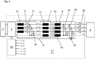
- FIG. 3 schematically illustrates an inverter assembly of the prior art and the FIG. 4 shows an alternative embodiment with additional output-side current sensors.
- FIG. 3 schematically a well-known by a standard device of the Applicant construction principle of an inverter 1 ', the electrical output power is preferably provided for feeding into a public alternating voltage network 6.
- a DC voltage source 5 is connected, which may be, for example, the solar generator of a photovoltaic system.
- an inverter bridge 2 The structure of an inverter bridge 2 is here assumed to be fundamentally known and therefore not described in detail at this point.
- the inverter bridge 2 has approximately an arrangement of three half-bridges, each consisting of two power semiconductor switches, which are controlled in clocked fashion by an electronic control circuit 10 'shown only schematically here.
- the relatively high clock frequencies of the drive pulses used in this case are largely filtered out by acting as a low-pass filter sine filter 3 on the phase conductors L1, L2, L3 of the inverter bridge 2.
- the sine-wave filter 3 has, for each phase conductor L1, L2, L3, a respective longitudinal choke 31 and a capacitor 32 connected to the neutral conductor N.
- the sine filter 3 shapes the pulses of the inverter output voltage to the desired sinusoidal shape.
- a choke coil arrangement 7 Connected downstream of the sine-wave filter 3 is a choke coil arrangement 7, which in each case has a choke coil 71 for each phase conductor L1, L2, L3 and also for the neutral conductor N.
- Each choke coil 71 consists of a separate choke coil core with a choke coil winding thereon.
- the phase coils L1, L2, L3 associated inductors 71 of the inductor assembly 7 thereby form with the longitudinal inductors 31 and Capacitors 32 of the sine filter 3 are each a so-called T-filter 8 'from.
- the purpose of the T-filter 8 ' is to give the inverter 1' a minimum impedance and thus also a natural frequency, which lies outside the frequency ranges for possible disturbing resonance effects.
- the EMC filter 4 is arranged, which consists of four co-directional inductor coils 41 on a common inductor core 40, which are turned on in the three phase conductors L1, L2, L3 and in the neutral conductor N.
- first capacitors 42 are connected between each phase conductor L1, L2, L3 and the neutral conductor N
- second capacitors 43 are connected between the phase conductors L1, L2, L3 and a ground potential M.
- the EMC filter 4 fulfills the function of a network filter which filters out electrical interference pulses between the inverter bridge 2 and the AC voltage network 6 in both directions.
- the drive circuit 10 ' is intended to generate, among other things, a desired phase angle between output current and mains voltage by driving the inverter bridge 2.
- current sensors 91 are provided inside the T-filter 8 ', which detect the time profiles of the currents iL1_wr, iL2_wr, iL3_wr in the three phase conductors L1, L2, L3 behind the first longitudinal inductors 31.
- the drive circuit 10 'estimates the position of the zero crossings of the voltages on the phase conductors L1, L2, L3 on the basis of the unfortunately imprecise known filter impedance.
- the components of the T-filter 8 are usually tolerances between 10% and 20% to assume.
- the filter impedance is a temperature-dependent variable. Accordingly, only a relative coarse determination of Voltage zero crossings possible. It follows with the in the FIG. 3 shown construction only a relatively inaccurate cos- ⁇ -Vor horrung realize.
- FIG. 4 shows the structure of an inverter 1 ", with which instead of a relatively inaccurate precontrol of the phase angle ⁇ an exact cos ⁇ control is possible.
- the Indian FIG. 1 shown inverter 1 solves the problems described above in a cost effective manner.
- the solution is that, according to the invention, an additional winding 83 is arranged on each line-side filter choke 82 of the T-filter 8.
- signal voltages uL1, uL2, uL3 proportional to the voltages on the phase conductors L1, L2, L3 can be taken, by means of which the voltage zero crossings of the phase voltages can be detected with high accuracy , Relative to these voltage zero crossings, taking into account the current profiles iL1_wr, iL2_wr, iL3_wr detected by the current sensors 9, the phase angles between output currents and output voltages of the individual phases can be determined and regulated.
- the drive circuit 10 advantageously has a circuit arrangement 100 for each phase conductor L1, L2, L3 according to FIG FIG. 2 on.
- the in the FIG. 2 sketched circuit 100 consists of a low-pass filter 110, a compressor circuit 120 and optionally from the compressor circuit 120 downstream expander 130th
- circuit components 110, 120, 130 are in the FIG. 2 in the form of essentially sketched as known basic circuits and therefore need not be explained in detail here.
- Worth mentioning are the anti-parallel diode arrangements in the feedback branch of the compressor circuit 120 and in the input branch of the expander circuit 130, which enables the function of the circuit for both positive and negative input voltages.
- the in the FIG. 2 schematically illustrated circuit arrangement is present once for each phase of the inverter 1.
- the index n added to the voltage signals is in the following representative of the indices 1, 2 and 3 of the three phase conductors L1, L2, L3.
- the input of the low-pass filter 110 the voltage uLn taken at one of the auxiliary windings 83 is supplied.
- this voltage signal uLn also contains a number of higher-frequency harmonics which originate from the higher-frequency (magnitude 20 kHz) drive pulses of the inverter bridge 2 originating from the drive circuit 10.
- These higher-frequency components are largely filtered out by the low-pass filter 110, so that the output voltage u_Filter_n of the low-pass filter 110 represents a substantially sinusoidal voltage with only a small interference voltage component.
- This output voltage u_Filter_n of the low-pass filter 110 is supplied to the compressor circuit 120 as an input voltage.
- the compressor circuit 120 structurally forms a logarithmizer, which forms the Input voltage nonlinear maps to a smaller range of values, which is well evaluated for a zero crossing detection, such as an unillustrated analog-to-digital converter.
- the expander 130 (Exponentierer) can optionally be followed by the compressor 120 to spread these special signal areas optional, by which the accuracy of the zero crossing detection can be further increased.
- the need for the expander circuit 130 is given only if the slope in the zero crossing, at maximum current, must be limited. Otherwise, only the low-pass filter 110 and the compressor circuit 120 are needed for signal conditioning.
- the drive circuit 10 internally calculates the phase shift between output current and output voltage from the detected zero point crossings of the voltages u_Komp_n or u_Exp_n and the current profiles iLn_wr detected by the current sensors 9 and accordingly influences the activation of the inverter bridge 2 to set the required reactive power supply.
Landscapes
- Engineering & Computer Science (AREA)
- Power Engineering (AREA)
- Inverter Devices (AREA)
Claims (5)
- Onduleur (1, 1', 1"),
avec un pont d'onduleur (2), qui, générant une tension alternative monophasée ou polyphasée, peut être relié, par l'intermédiaire d'un ou de plusieurs conducteur/s de phase (L1, L2, L3) et d'un conducteur neutre (N), à un réseau de tension alternative (6) et
avec un filtre en T (8, 8'), qui, connecté en aval du pont d'onduleur (2), consiste en deux inductances longitudinales, (31, 71 ; 81, 82), connectées en cascade pour chacun des conducteur/s de phase (L1, L2, L3), au point de jonction desquelles est respectivement appliqué un raccord d'un condensateur (32, 84), dont le deuxième raccord est connecté contre le conducteur neutre (N),
caractérisé en ce que
les inductances longitudinales (82) du filtre en T (8) côté réseau, présentent chacune un enroulement supplémentaire (83), sur lesquels, par un circuit d'excitation (10), une tension de signal (uL1, uL2, uL3) est respectivement saisie pour influencer le pont d'onduleur (2). - Onduleur selon la revendication 1, caractérisé en ce que les tensions de signal (uL1, uL2, uL3) sont traitées chacune par un circuit de commutation (100), qui présente au moins un filtre passe-bas (110) et un circuit de compresseur (120).
- Onduleur selon la revendication 2, caractérisé en ce que, en aval du circuit de compresseur (120), est connecté un circuit d'expanseur (130).
- Onduleur selon revendication 2 ou 3, caractérisé en ce que le circuit de commutation (100) est composant d'un circuit de commande (10) pour la commande du pont d'onduleur (2).
- Onduleur selon la revendication 1, caractérisé en ce que l'onduleur (1) est composant d'une installation photovoltaïque.
Applications Claiming Priority (1)
| Application Number | Priority Date | Filing Date | Title |
|---|---|---|---|
| DE102015005992.0A DE102015005992A1 (de) | 2015-05-08 | 2015-05-08 | Wechselrichter |
Publications (2)
| Publication Number | Publication Date |
|---|---|
| EP3091649A1 EP3091649A1 (fr) | 2016-11-09 |
| EP3091649B1 true EP3091649B1 (fr) | 2018-02-28 |
Family
ID=55910858
Family Applications (1)
| Application Number | Title | Priority Date | Filing Date |
|---|---|---|---|
| EP16168186.1A Active EP3091649B1 (fr) | 2015-05-08 | 2016-05-03 | Onduleur |
Country Status (2)
| Country | Link |
|---|---|
| EP (1) | EP3091649B1 (fr) |
| DE (1) | DE102015005992A1 (fr) |
Family Cites Families (4)
| Publication number | Priority date | Publication date | Assignee | Title |
|---|---|---|---|---|
| DE102009029387A1 (de) | 2009-09-11 | 2011-03-24 | Robert Bosch Gmbh | DC-AC-Wechselrichteranordnung, insbesondere Solarzelleninverter |
| CN102223094B (zh) * | 2010-04-16 | 2014-04-09 | 通用电气公司 | 电力转换系统及其中lc电路阻尼方法 |
| US9312753B2 (en) * | 2013-07-02 | 2016-04-12 | Delta Electronics (Shanghai) Co., Ltd. | Power converter with low common mode noise |
| US9729085B2 (en) * | 2014-09-26 | 2017-08-08 | Majid Pahlevaninezhad | Observer-based control system for grid-connected DC/AC converters with LCL-filter |
-
2015
- 2015-05-08 DE DE102015005992.0A patent/DE102015005992A1/de not_active Withdrawn
-
2016
- 2016-05-03 EP EP16168186.1A patent/EP3091649B1/fr active Active
Also Published As
| Publication number | Publication date |
|---|---|
| DE102015005992A1 (de) | 2016-11-10 |
| EP3091649A1 (fr) | 2016-11-09 |
Similar Documents
| Publication | Publication Date | Title |
|---|---|---|
| EP2030299B1 (fr) | Onduleur destiné à injecter de l'énergie électrique dans un réseau de distribution d'énergie | |
| DE102012102209A1 (de) | Netzgekoppelter Wechselrichter, Wechselrichteranordnung und Betriebsverfahren für eine Wechselrichteranordnung | |
| DE112013006680T5 (de) | Dreiphasen-Spannungs-Umsetzungsvorrichtung | |
| EP2697661A1 (fr) | Procédé et dispositif de détermination d'une composante de courant de défaut à un courant différentiel | |
| DE2225609C2 (de) | Anordnung zur Steuerung der Drehzahl eines über einen statischen Umrichter mit variabler Spannung und dazu etwa mit proportionaler Frequenz gespeisten Mehrphasenwechselstrom-Asynchronmotors | |
| EP1598924B1 (fr) | Ondueur sans harmoniques | |
| EP4046268A1 (fr) | Détermination de paramètres de filtre dans un onduleur | |
| DE2803839A1 (de) | Wechselstrom-steuersystem fuer wechselstrom-versorgung | |
| DE102016116630A1 (de) | Verfahren zum Betrieb eines Wechselrichters und Wechselrichter | |
| DE102013212426A1 (de) | Umrichteranordnung mit parallel geschalteten Mehrstufen-Umrichtern sowie Verfahren zu deren Steuerung | |
| EP0208088B1 (fr) | Dispositif pur l'obtention d'un système de tensions triphasées avec conducteur neutre chargeable | |
| EP2367272B1 (fr) | Onduleur | |
| DE3810870A1 (de) | Vorrichtung zum umformen von elektrischer energie | |
| EP3091649B1 (fr) | Onduleur | |
| DE102014111451A1 (de) | System zur Anhebung des netzseitigen Leistungsfaktors von dreiphasig gespeisten EC-Motoren | |
| DE102017005928A1 (de) | Umrichtersystem und Verfahren zum Betreiben eines Umrichtersystems | |
| DE3437242A1 (de) | Elektronischer leistungssteller, insbesondere zur regelung der auslauftemperatur bei elektrischen durchlauferhitzern | |
| DE69205476T2 (de) | Verfahren und Vorrichtung zum Dämpfen des Funkstörungseffektes auf Leitern im mehrphasigen Wechselstromnetz. | |
| DE10249122A1 (de) | Vorrichtung und Verfahren zur Unterdrückung eines Gleichstromanteiles im Ausgangsstrom von Wechselrichtern | |
| EP3459165B1 (fr) | Convertisseur et procédé de fonctionnement de celui-ci | |
| EP4115511A1 (fr) | Ensemble convertisseur | |
| DE102013200520A1 (de) | Wechselrichteranordnung und Verfahren zum Erzeugen eines elektrischen Wechselstroms | |
| DE102013219530A1 (de) | Ermittlung eines Stromnulldurchgangs eines Wechselstroms | |
| CH708040A2 (de) | Elektronischer Leistungswandler und Verfahren zu dessen Ansteuerung. | |
| EP2026455B1 (fr) | Procédé de fonctionnement d'une commutation électrique et commutation électrique destinée à éviter les surtensions sur des charges alimentées en sens inverses |
Legal Events
| Date | Code | Title | Description |
|---|---|---|---|
| PUAI | Public reference made under article 153(3) epc to a published international application that has entered the european phase |
Free format text: ORIGINAL CODE: 0009012 |
|
| AK | Designated contracting states |
Kind code of ref document: A1 Designated state(s): AL AT BE BG CH CY CZ DE DK EE ES FI FR GB GR HR HU IE IS IT LI LT LU LV MC MK MT NL NO PL PT RO RS SE SI SK SM TR |
|
| AX | Request for extension of the european patent |
Extension state: BA ME |
|
| 17P | Request for examination filed |
Effective date: 20170418 |
|
| GRAP | Despatch of communication of intention to grant a patent |
Free format text: ORIGINAL CODE: EPIDOSNIGR1 |
|
| INTG | Intention to grant announced |
Effective date: 20171212 |
|
| GRAS | Grant fee paid |
Free format text: ORIGINAL CODE: EPIDOSNIGR3 |
|
| GRAA | (expected) grant |
Free format text: ORIGINAL CODE: 0009210 |
|
| AK | Designated contracting states |
Kind code of ref document: B1 Designated state(s): AL AT BE BG CH CY CZ DE DK EE ES FI FR GB GR HR HU IE IS IT LI LT LU LV MC MK MT NL NO PL PT RO RS SE SI SK SM TR |
|
| REG | Reference to a national code |
Ref country code: GB Ref legal event code: FG4D Free format text: NOT ENGLISH Ref country code: CH Ref legal event code: EP |
|
| REG | Reference to a national code |
Ref country code: AT Ref legal event code: REF Ref document number: 975158 Country of ref document: AT Kind code of ref document: T Effective date: 20180315 |
|
| REG | Reference to a national code |
Ref country code: IE Ref legal event code: FG4D Free format text: LANGUAGE OF EP DOCUMENT: GERMAN |
|
| REG | Reference to a national code |
Ref country code: DE Ref legal event code: R096 Ref document number: 502016000603 Country of ref document: DE |
|
| REG | Reference to a national code |
Ref country code: FR Ref legal event code: PLFP Year of fee payment: 3 |
|
| REG | Reference to a national code |
Ref country code: NL Ref legal event code: MP Effective date: 20180228 |
|
| REG | Reference to a national code |
Ref country code: LT Ref legal event code: MG4D |
|
| PG25 | Lapsed in a contracting state [announced via postgrant information from national office to epo] |
Ref country code: ES Free format text: LAPSE BECAUSE OF FAILURE TO SUBMIT A TRANSLATION OF THE DESCRIPTION OR TO PAY THE FEE WITHIN THE PRESCRIBED TIME-LIMIT Effective date: 20180228 Ref country code: NL Free format text: LAPSE BECAUSE OF FAILURE TO SUBMIT A TRANSLATION OF THE DESCRIPTION OR TO PAY THE FEE WITHIN THE PRESCRIBED TIME-LIMIT Effective date: 20180228 Ref country code: CY Free format text: LAPSE BECAUSE OF FAILURE TO SUBMIT A TRANSLATION OF THE DESCRIPTION OR TO PAY THE FEE WITHIN THE PRESCRIBED TIME-LIMIT Effective date: 20180228 Ref country code: FI Free format text: LAPSE BECAUSE OF FAILURE TO SUBMIT A TRANSLATION OF THE DESCRIPTION OR TO PAY THE FEE WITHIN THE PRESCRIBED TIME-LIMIT Effective date: 20180228 Ref country code: NO Free format text: LAPSE BECAUSE OF FAILURE TO SUBMIT A TRANSLATION OF THE DESCRIPTION OR TO PAY THE FEE WITHIN THE PRESCRIBED TIME-LIMIT Effective date: 20180528 Ref country code: LT Free format text: LAPSE BECAUSE OF FAILURE TO SUBMIT A TRANSLATION OF THE DESCRIPTION OR TO PAY THE FEE WITHIN THE PRESCRIBED TIME-LIMIT Effective date: 20180228 Ref country code: HR Free format text: LAPSE BECAUSE OF FAILURE TO SUBMIT A TRANSLATION OF THE DESCRIPTION OR TO PAY THE FEE WITHIN THE PRESCRIBED TIME-LIMIT Effective date: 20180228 |
|
| PG25 | Lapsed in a contracting state [announced via postgrant information from national office to epo] |
Ref country code: BG Free format text: LAPSE BECAUSE OF FAILURE TO SUBMIT A TRANSLATION OF THE DESCRIPTION OR TO PAY THE FEE WITHIN THE PRESCRIBED TIME-LIMIT Effective date: 20180528 Ref country code: RS Free format text: LAPSE BECAUSE OF FAILURE TO SUBMIT A TRANSLATION OF THE DESCRIPTION OR TO PAY THE FEE WITHIN THE PRESCRIBED TIME-LIMIT Effective date: 20180228 Ref country code: LV Free format text: LAPSE BECAUSE OF FAILURE TO SUBMIT A TRANSLATION OF THE DESCRIPTION OR TO PAY THE FEE WITHIN THE PRESCRIBED TIME-LIMIT Effective date: 20180228 Ref country code: SE Free format text: LAPSE BECAUSE OF FAILURE TO SUBMIT A TRANSLATION OF THE DESCRIPTION OR TO PAY THE FEE WITHIN THE PRESCRIBED TIME-LIMIT Effective date: 20180228 Ref country code: GR Free format text: LAPSE BECAUSE OF FAILURE TO SUBMIT A TRANSLATION OF THE DESCRIPTION OR TO PAY THE FEE WITHIN THE PRESCRIBED TIME-LIMIT Effective date: 20180529 |
|
| PG25 | Lapsed in a contracting state [announced via postgrant information from national office to epo] |
Ref country code: MT Free format text: LAPSE BECAUSE OF FAILURE TO SUBMIT A TRANSLATION OF THE DESCRIPTION OR TO PAY THE FEE WITHIN THE PRESCRIBED TIME-LIMIT Effective date: 20180228 |
|
| PG25 | Lapsed in a contracting state [announced via postgrant information from national office to epo] |
Ref country code: RO Free format text: LAPSE BECAUSE OF FAILURE TO SUBMIT A TRANSLATION OF THE DESCRIPTION OR TO PAY THE FEE WITHIN THE PRESCRIBED TIME-LIMIT Effective date: 20180228 Ref country code: IT Free format text: LAPSE BECAUSE OF FAILURE TO SUBMIT A TRANSLATION OF THE DESCRIPTION OR TO PAY THE FEE WITHIN THE PRESCRIBED TIME-LIMIT Effective date: 20180228 Ref country code: PL Free format text: LAPSE BECAUSE OF FAILURE TO SUBMIT A TRANSLATION OF THE DESCRIPTION OR TO PAY THE FEE WITHIN THE PRESCRIBED TIME-LIMIT Effective date: 20180228 Ref country code: EE Free format text: LAPSE BECAUSE OF FAILURE TO SUBMIT A TRANSLATION OF THE DESCRIPTION OR TO PAY THE FEE WITHIN THE PRESCRIBED TIME-LIMIT Effective date: 20180228 Ref country code: AL Free format text: LAPSE BECAUSE OF FAILURE TO SUBMIT A TRANSLATION OF THE DESCRIPTION OR TO PAY THE FEE WITHIN THE PRESCRIBED TIME-LIMIT Effective date: 20180228 |
|
| REG | Reference to a national code |
Ref country code: DE Ref legal event code: R097 Ref document number: 502016000603 Country of ref document: DE |
|
| PG25 | Lapsed in a contracting state [announced via postgrant information from national office to epo] |
Ref country code: SM Free format text: LAPSE BECAUSE OF FAILURE TO SUBMIT A TRANSLATION OF THE DESCRIPTION OR TO PAY THE FEE WITHIN THE PRESCRIBED TIME-LIMIT Effective date: 20180228 Ref country code: DK Free format text: LAPSE BECAUSE OF FAILURE TO SUBMIT A TRANSLATION OF THE DESCRIPTION OR TO PAY THE FEE WITHIN THE PRESCRIBED TIME-LIMIT Effective date: 20180228 Ref country code: CZ Free format text: LAPSE BECAUSE OF FAILURE TO SUBMIT A TRANSLATION OF THE DESCRIPTION OR TO PAY THE FEE WITHIN THE PRESCRIBED TIME-LIMIT Effective date: 20180228 Ref country code: SK Free format text: LAPSE BECAUSE OF FAILURE TO SUBMIT A TRANSLATION OF THE DESCRIPTION OR TO PAY THE FEE WITHIN THE PRESCRIBED TIME-LIMIT Effective date: 20180228 |
|
| PLBE | No opposition filed within time limit |
Free format text: ORIGINAL CODE: 0009261 |
|
| STAA | Information on the status of an ep patent application or granted ep patent |
Free format text: STATUS: NO OPPOSITION FILED WITHIN TIME LIMIT |
|
| REG | Reference to a national code |
Ref country code: BE Ref legal event code: MM Effective date: 20180531 |
|
| PG25 | Lapsed in a contracting state [announced via postgrant information from national office to epo] |
Ref country code: MC Free format text: LAPSE BECAUSE OF FAILURE TO SUBMIT A TRANSLATION OF THE DESCRIPTION OR TO PAY THE FEE WITHIN THE PRESCRIBED TIME-LIMIT Effective date: 20180228 |
|
| 26N | No opposition filed |
Effective date: 20181129 |
|
| REG | Reference to a national code |
Ref country code: IE Ref legal event code: MM4A |
|
| PG25 | Lapsed in a contracting state [announced via postgrant information from national office to epo] |
Ref country code: SI Free format text: LAPSE BECAUSE OF FAILURE TO SUBMIT A TRANSLATION OF THE DESCRIPTION OR TO PAY THE FEE WITHIN THE PRESCRIBED TIME-LIMIT Effective date: 20180228 |
|
| PG25 | Lapsed in a contracting state [announced via postgrant information from national office to epo] |
Ref country code: LU Free format text: LAPSE BECAUSE OF NON-PAYMENT OF DUE FEES Effective date: 20180503 |
|
| PG25 | Lapsed in a contracting state [announced via postgrant information from national office to epo] |
Ref country code: IE Free format text: LAPSE BECAUSE OF NON-PAYMENT OF DUE FEES Effective date: 20180503 |
|
| PG25 | Lapsed in a contracting state [announced via postgrant information from national office to epo] |
Ref country code: BE Free format text: LAPSE BECAUSE OF NON-PAYMENT OF DUE FEES Effective date: 20180531 |
|
| REG | Reference to a national code |
Ref country code: CH Ref legal event code: PL |
|
| PG25 | Lapsed in a contracting state [announced via postgrant information from national office to epo] |
Ref country code: LI Free format text: LAPSE BECAUSE OF NON-PAYMENT OF DUE FEES Effective date: 20190531 Ref country code: CH Free format text: LAPSE BECAUSE OF NON-PAYMENT OF DUE FEES Effective date: 20190531 |
|
| PG25 | Lapsed in a contracting state [announced via postgrant information from national office to epo] |
Ref country code: TR Free format text: LAPSE BECAUSE OF FAILURE TO SUBMIT A TRANSLATION OF THE DESCRIPTION OR TO PAY THE FEE WITHIN THE PRESCRIBED TIME-LIMIT Effective date: 20180228 |
|
| PG25 | Lapsed in a contracting state [announced via postgrant information from national office to epo] |
Ref country code: PT Free format text: LAPSE BECAUSE OF FAILURE TO SUBMIT A TRANSLATION OF THE DESCRIPTION OR TO PAY THE FEE WITHIN THE PRESCRIBED TIME-LIMIT Effective date: 20180228 |
|
| PG25 | Lapsed in a contracting state [announced via postgrant information from national office to epo] |
Ref country code: MK Free format text: LAPSE BECAUSE OF NON-PAYMENT OF DUE FEES Effective date: 20180228 Ref country code: HU Free format text: LAPSE BECAUSE OF FAILURE TO SUBMIT A TRANSLATION OF THE DESCRIPTION OR TO PAY THE FEE WITHIN THE PRESCRIBED TIME-LIMIT; INVALID AB INITIO Effective date: 20160503 |
|
| PG25 | Lapsed in a contracting state [announced via postgrant information from national office to epo] |
Ref country code: IS Free format text: LAPSE BECAUSE OF FAILURE TO SUBMIT A TRANSLATION OF THE DESCRIPTION OR TO PAY THE FEE WITHIN THE PRESCRIBED TIME-LIMIT Effective date: 20180628 |
|
| REG | Reference to a national code |
Ref country code: AT Ref legal event code: MM01 Ref document number: 975158 Country of ref document: AT Kind code of ref document: T Effective date: 20210503 |
|
| PG25 | Lapsed in a contracting state [announced via postgrant information from national office to epo] |
Ref country code: AT Free format text: LAPSE BECAUSE OF NON-PAYMENT OF DUE FEES Effective date: 20210503 |
|
| REG | Reference to a national code |
Ref country code: DE Ref legal event code: R081 Ref document number: 502016000603 Country of ref document: DE Owner name: KOSTAL INDUSTRIE ELEKTRIK GMBH & CO. KG, DE Free format text: FORMER OWNER: KOSTAL INDUSTRIE ELEKTRIK GMBH, 58513 LUEDENSCHEID, DE |
|
| PGFP | Annual fee paid to national office [announced via postgrant information from national office to epo] |
Ref country code: DE Payment date: 20250415 Year of fee payment: 10 |
|
| PGFP | Annual fee paid to national office [announced via postgrant information from national office to epo] |
Ref country code: GB Payment date: 20250410 Year of fee payment: 10 |
|
| PGFP | Annual fee paid to national office [announced via postgrant information from national office to epo] |
Ref country code: FR Payment date: 20250530 Year of fee payment: 10 |