EP3093835A1 - Pixel et affichage électroluminescent organique l'utilisant - Google Patents
Pixel et affichage électroluminescent organique l'utilisant Download PDFInfo
- Publication number
- EP3093835A1 EP3093835A1 EP16176868.4A EP16176868A EP3093835A1 EP 3093835 A1 EP3093835 A1 EP 3093835A1 EP 16176868 A EP16176868 A EP 16176868A EP 3093835 A1 EP3093835 A1 EP 3093835A1
- Authority
- EP
- European Patent Office
- Prior art keywords
- transistor
- light emitting
- organic light
- coupled
- driver
- Prior art date
- Legal status (The legal status is an assumption and is not a legal conclusion. Google has not performed a legal analysis and makes no representation as to the accuracy of the status listed.)
- Granted
Links
Images






Classifications
-
- G—PHYSICS
- G09—EDUCATION; CRYPTOGRAPHY; DISPLAY; ADVERTISING; SEALS
- G09G—ARRANGEMENTS OR CIRCUITS FOR CONTROL OF INDICATING DEVICES USING STATIC MEANS TO PRESENT VARIABLE INFORMATION
- G09G3/00—Control arrangements or circuits, of interest only in connection with visual indicators other than cathode-ray tubes
- G09G3/20—Control arrangements or circuits, of interest only in connection with visual indicators other than cathode-ray tubes for presentation of an assembly of a number of characters, e.g. a page, by composing the assembly by combination of individual elements arranged in a matrix no fixed position being assigned to or needed to be assigned to the individual characters or partial characters
- G09G3/22—Control arrangements or circuits, of interest only in connection with visual indicators other than cathode-ray tubes for presentation of an assembly of a number of characters, e.g. a page, by composing the assembly by combination of individual elements arranged in a matrix no fixed position being assigned to or needed to be assigned to the individual characters or partial characters using controlled light sources
- G09G3/30—Control arrangements or circuits, of interest only in connection with visual indicators other than cathode-ray tubes for presentation of an assembly of a number of characters, e.g. a page, by composing the assembly by combination of individual elements arranged in a matrix no fixed position being assigned to or needed to be assigned to the individual characters or partial characters using controlled light sources using electroluminescent panels
- G09G3/32—Control arrangements or circuits, of interest only in connection with visual indicators other than cathode-ray tubes for presentation of an assembly of a number of characters, e.g. a page, by composing the assembly by combination of individual elements arranged in a matrix no fixed position being assigned to or needed to be assigned to the individual characters or partial characters using controlled light sources using electroluminescent panels semiconductive, e.g. using light-emitting diodes [LED]
- G09G3/3208—Control arrangements or circuits, of interest only in connection with visual indicators other than cathode-ray tubes for presentation of an assembly of a number of characters, e.g. a page, by composing the assembly by combination of individual elements arranged in a matrix no fixed position being assigned to or needed to be assigned to the individual characters or partial characters using controlled light sources using electroluminescent panels semiconductive, e.g. using light-emitting diodes [LED] organic, e.g. using organic light-emitting diodes [OLED]
- G09G3/3225—Control arrangements or circuits, of interest only in connection with visual indicators other than cathode-ray tubes for presentation of an assembly of a number of characters, e.g. a page, by composing the assembly by combination of individual elements arranged in a matrix no fixed position being assigned to or needed to be assigned to the individual characters or partial characters using controlled light sources using electroluminescent panels semiconductive, e.g. using light-emitting diodes [LED] organic, e.g. using organic light-emitting diodes [OLED] using an active matrix
- G09G3/3233—Control arrangements or circuits, of interest only in connection with visual indicators other than cathode-ray tubes for presentation of an assembly of a number of characters, e.g. a page, by composing the assembly by combination of individual elements arranged in a matrix no fixed position being assigned to or needed to be assigned to the individual characters or partial characters using controlled light sources using electroluminescent panels semiconductive, e.g. using light-emitting diodes [LED] organic, e.g. using organic light-emitting diodes [OLED] using an active matrix with pixel circuitry controlling the current through the light-emitting element
- G09G3/3241—Control arrangements or circuits, of interest only in connection with visual indicators other than cathode-ray tubes for presentation of an assembly of a number of characters, e.g. a page, by composing the assembly by combination of individual elements arranged in a matrix no fixed position being assigned to or needed to be assigned to the individual characters or partial characters using controlled light sources using electroluminescent panels semiconductive, e.g. using light-emitting diodes [LED] organic, e.g. using organic light-emitting diodes [OLED] using an active matrix with pixel circuitry controlling the current through the light-emitting element the current through the light-emitting element being set using a data current provided by the data driver, e.g. by using a two-transistor current mirror
-
- G—PHYSICS
- G09—EDUCATION; CRYPTOGRAPHY; DISPLAY; ADVERTISING; SEALS
- G09G—ARRANGEMENTS OR CIRCUITS FOR CONTROL OF INDICATING DEVICES USING STATIC MEANS TO PRESENT VARIABLE INFORMATION
- G09G3/00—Control arrangements or circuits, of interest only in connection with visual indicators other than cathode-ray tubes
- G09G3/20—Control arrangements or circuits, of interest only in connection with visual indicators other than cathode-ray tubes for presentation of an assembly of a number of characters, e.g. a page, by composing the assembly by combination of individual elements arranged in a matrix no fixed position being assigned to or needed to be assigned to the individual characters or partial characters
- G09G3/22—Control arrangements or circuits, of interest only in connection with visual indicators other than cathode-ray tubes for presentation of an assembly of a number of characters, e.g. a page, by composing the assembly by combination of individual elements arranged in a matrix no fixed position being assigned to or needed to be assigned to the individual characters or partial characters using controlled light sources
- G09G3/30—Control arrangements or circuits, of interest only in connection with visual indicators other than cathode-ray tubes for presentation of an assembly of a number of characters, e.g. a page, by composing the assembly by combination of individual elements arranged in a matrix no fixed position being assigned to or needed to be assigned to the individual characters or partial characters using controlled light sources using electroluminescent panels
- G09G3/32—Control arrangements or circuits, of interest only in connection with visual indicators other than cathode-ray tubes for presentation of an assembly of a number of characters, e.g. a page, by composing the assembly by combination of individual elements arranged in a matrix no fixed position being assigned to or needed to be assigned to the individual characters or partial characters using controlled light sources using electroluminescent panels semiconductive, e.g. using light-emitting diodes [LED]
- G09G3/3208—Control arrangements or circuits, of interest only in connection with visual indicators other than cathode-ray tubes for presentation of an assembly of a number of characters, e.g. a page, by composing the assembly by combination of individual elements arranged in a matrix no fixed position being assigned to or needed to be assigned to the individual characters or partial characters using controlled light sources using electroluminescent panels semiconductive, e.g. using light-emitting diodes [LED] organic, e.g. using organic light-emitting diodes [OLED]
- G09G3/3225—Control arrangements or circuits, of interest only in connection with visual indicators other than cathode-ray tubes for presentation of an assembly of a number of characters, e.g. a page, by composing the assembly by combination of individual elements arranged in a matrix no fixed position being assigned to or needed to be assigned to the individual characters or partial characters using controlled light sources using electroluminescent panels semiconductive, e.g. using light-emitting diodes [LED] organic, e.g. using organic light-emitting diodes [OLED] using an active matrix
- G09G3/3233—Control arrangements or circuits, of interest only in connection with visual indicators other than cathode-ray tubes for presentation of an assembly of a number of characters, e.g. a page, by composing the assembly by combination of individual elements arranged in a matrix no fixed position being assigned to or needed to be assigned to the individual characters or partial characters using controlled light sources using electroluminescent panels semiconductive, e.g. using light-emitting diodes [LED] organic, e.g. using organic light-emitting diodes [OLED] using an active matrix with pixel circuitry controlling the current through the light-emitting element
-
- G—PHYSICS
- G09—EDUCATION; CRYPTOGRAPHY; DISPLAY; ADVERTISING; SEALS
- G09G—ARRANGEMENTS OR CIRCUITS FOR CONTROL OF INDICATING DEVICES USING STATIC MEANS TO PRESENT VARIABLE INFORMATION
- G09G2300/00—Aspects of the constitution of display devices
- G09G2300/08—Active matrix structure, i.e. with use of active elements, inclusive of non-linear two terminal elements, in the pixels together with light emitting or modulating elements
- G09G2300/0809—Several active elements per pixel in active matrix panels
- G09G2300/0819—Several active elements per pixel in active matrix panels used for counteracting undesired variations, e.g. feedback or autozeroing
-
- G—PHYSICS
- G09—EDUCATION; CRYPTOGRAPHY; DISPLAY; ADVERTISING; SEALS
- G09G—ARRANGEMENTS OR CIRCUITS FOR CONTROL OF INDICATING DEVICES USING STATIC MEANS TO PRESENT VARIABLE INFORMATION
- G09G2300/00—Aspects of the constitution of display devices
- G09G2300/08—Active matrix structure, i.e. with use of active elements, inclusive of non-linear two terminal elements, in the pixels together with light emitting or modulating elements
- G09G2300/0809—Several active elements per pixel in active matrix panels
- G09G2300/0842—Several active elements per pixel in active matrix panels forming a memory circuit, e.g. a dynamic memory with one capacitor
- G09G2300/0852—Several active elements per pixel in active matrix panels forming a memory circuit, e.g. a dynamic memory with one capacitor being a dynamic memory with more than one capacitor
-
- G—PHYSICS
- G09—EDUCATION; CRYPTOGRAPHY; DISPLAY; ADVERTISING; SEALS
- G09G—ARRANGEMENTS OR CIRCUITS FOR CONTROL OF INDICATING DEVICES USING STATIC MEANS TO PRESENT VARIABLE INFORMATION
- G09G2300/00—Aspects of the constitution of display devices
- G09G2300/08—Active matrix structure, i.e. with use of active elements, inclusive of non-linear two terminal elements, in the pixels together with light emitting or modulating elements
- G09G2300/0809—Several active elements per pixel in active matrix panels
- G09G2300/0842—Several active elements per pixel in active matrix panels forming a memory circuit, e.g. a dynamic memory with one capacitor
- G09G2300/0861—Several active elements per pixel in active matrix panels forming a memory circuit, e.g. a dynamic memory with one capacitor with additional control of the display period without amending the charge stored in a pixel memory, e.g. by means of additional select electrodes
-
- G—PHYSICS
- G09—EDUCATION; CRYPTOGRAPHY; DISPLAY; ADVERTISING; SEALS
- G09G—ARRANGEMENTS OR CIRCUITS FOR CONTROL OF INDICATING DEVICES USING STATIC MEANS TO PRESENT VARIABLE INFORMATION
- G09G2310/00—Command of the display device
- G09G2310/02—Addressing, scanning or driving the display screen or processing steps related thereto
- G09G2310/0243—Details of the generation of driving signals
- G09G2310/0245—Clearing or presetting the whole screen independently of waveforms, e.g. on power-on
-
- G—PHYSICS
- G09—EDUCATION; CRYPTOGRAPHY; DISPLAY; ADVERTISING; SEALS
- G09G—ARRANGEMENTS OR CIRCUITS FOR CONTROL OF INDICATING DEVICES USING STATIC MEANS TO PRESENT VARIABLE INFORMATION
- G09G2310/00—Command of the display device
- G09G2310/02—Addressing, scanning or driving the display screen or processing steps related thereto
- G09G2310/0243—Details of the generation of driving signals
- G09G2310/0251—Precharge or discharge of pixel before applying new pixel voltage
-
- G—PHYSICS
- G09—EDUCATION; CRYPTOGRAPHY; DISPLAY; ADVERTISING; SEALS
- G09G—ARRANGEMENTS OR CIRCUITS FOR CONTROL OF INDICATING DEVICES USING STATIC MEANS TO PRESENT VARIABLE INFORMATION
- G09G2320/00—Control of display operating conditions
- G09G2320/02—Improving the quality of display appearance
- G09G2320/0233—Improving the luminance or brightness uniformity across the screen
-
- G—PHYSICS
- G09—EDUCATION; CRYPTOGRAPHY; DISPLAY; ADVERTISING; SEALS
- G09G—ARRANGEMENTS OR CIRCUITS FOR CONTROL OF INDICATING DEVICES USING STATIC MEANS TO PRESENT VARIABLE INFORMATION
- G09G2320/00—Control of display operating conditions
- G09G2320/04—Maintaining the quality of display appearance
- G09G2320/043—Preventing or counteracting the effects of ageing
-
- G—PHYSICS
- G09—EDUCATION; CRYPTOGRAPHY; DISPLAY; ADVERTISING; SEALS
- G09G—ARRANGEMENTS OR CIRCUITS FOR CONTROL OF INDICATING DEVICES USING STATIC MEANS TO PRESENT VARIABLE INFORMATION
- G09G2320/00—Control of display operating conditions
- G09G2320/04—Maintaining the quality of display appearance
- G09G2320/043—Preventing or counteracting the effects of ageing
- G09G2320/045—Compensation of drifts in the characteristics of light emitting or modulating elements
-
- G—PHYSICS
- G09—EDUCATION; CRYPTOGRAPHY; DISPLAY; ADVERTISING; SEALS
- G09G—ARRANGEMENTS OR CIRCUITS FOR CONTROL OF INDICATING DEVICES USING STATIC MEANS TO PRESENT VARIABLE INFORMATION
- G09G2360/00—Aspects of the architecture of display systems
- G09G2360/14—Detecting light within display terminals, e.g. using a single or a plurality of photosensors
- G09G2360/145—Detecting light within display terminals, e.g. using a single or a plurality of photosensors the light originating from the display screen
- G09G2360/147—Detecting light within display terminals, e.g. using a single or a plurality of photosensors the light originating from the display screen the originated light output being determined for each pixel
- G09G2360/148—Detecting light within display terminals, e.g. using a single or a plurality of photosensors the light originating from the display screen the originated light output being determined for each pixel the light being detected by light detection means within each pixel
Definitions
- Embodiments of the present invention relate to a pixel and an organic light emitting display using the same.
- FPDs flat panel displays
- LCD liquid crystal display
- organic light emitting display and a plasma display panel
- An organic light emitting display displays images using organic light emitting diodes that emit light through recombination of electrons and holes.
- the organic light emitting display has a fast response speed and has low power consumption.
- Background prior art in the field is disclosed in US 2012/113077A1 , EP 2 463 849 A1 , EP 2 146 337 A1 , US 2011/279484 A1 , US 2008/243498 A1 und US 2011/090200 A1 , for instance.
- the present invention provides a pixel according to claim 1 and an organic light emitting display according to claim 10 using the same, which can be at least driven at a low frequency.
- Advantageous embodiments are provided in the dependent claims.
- a pixel including: an organic light emitting diode; a second driver configured to control an amount of current supplied from a first power source to the organic light emitting diode, corresponding to a previous data signal; and a first driver configured to store a current data signal supplied from a data line and supply the previous data signal to the second driver, wherein the second driver includes: a sixth transistor coupled between an initialization power source and a first node coupled to a gate electrode of a first transistor, the sixth transistor being configured to turn on when a first control signal is supplied to a first control line; and a seventh transistor coupled between the first power source and a second node commonly coupled to the first and second drivers, the seventh transistor being configured to turn on when the first control signal is supplied.
- the initialization power source may be set to a voltage lower than the data signal supplied to the data line.
- the first driver may include a second transistor coupled between the data line and a third node, the second transistor being configured to turn on when a scan signal is supplied to a scan line; a third transistor coupled between the third and second nodes, the third transistor being configured to turn on when a second control signal is supplied; and a second capacitor coupled between the third node and the initialization power source.
- the third and sixth transistors may have turn-on periods not overlapped with each other.
- the second transistor may have a turn-on period not overlapped with those of the third and sixth transistors.
- the second driver may include an eighth transistor coupled between the first power source and the second node coupled to a first electrode of the first transistor, the eighth transistor being configured to turn off when an emission control signal is supplied and to turn on otherwise; a fifth transistor coupled between the first node and a second electrode of the first transistor, the fifth transistor being configured to turn on when the second control signal is supplied; a ninth transistor coupled between the second electrode of the first transistor and an anode electrode of the organic light emitting diode, the ninth transistor being configured to turn off when the emission control signal is supplied and to turn on otherwise; and a first capacitor coupled between the first node and the first power source.
- the eighth transistor may have a turn-on period not overlapped with those of the fifth and sixth transistors.
- the fifth and sixth transistors may have turn-on periods not overlapped with each other.
- the second driver may further include a fourth transistor coupled between the anode electrode of the organic light emitting diode and the initialization power source, the fourth transistor being configured to turn on when the first control signal is supplied.
- the second driver may further include a fourth transistor coupled between the anode electrode of the organic light emitting diode and the initialization power source, the fourth transistor being configured to turn on when the second control signal is supplied.
- the second driver may further include a fourth transistor positioned between the anode electrode of the organic light emitting diode and a second control line to which the second control signal is supplied, the fourth transistor having a gate electrode coupled to the second control line.
- the second driver may further include a photodiode coupled in parallel to the first capacitor between the first node and the first power source.
- the photodiode may control the increment of the voltage at the first node, corresponding to the luminance of the organic light emitting diode.
- the photodiode may control the increment of the voltage at the first node, in proportion to the luminance of the organic light emitting diode.
- the second driver may further include a third capacitor coupled between the anode electrode of the organic light emitting diode and the second node.
- an organic light emitting display including: a control driver configured to supply a first control signal to a first control line, and to supply a second control signal to a second control line during a first period in one frame; a scan driver configured to supply an emission control line to an emission control line during the first period, a second period and a third period in the one frame, and progressively supply a scan signal to scan lines during a fourth period in the one frame; a data driver configured to supply a data signal to data lines, in synchronization with the scan signal, during the fourth period in the one frame; and pixels positioned in an area defined by the scan lines and the data lines, the pixels storing a current data signal during a period in which the pixels emit light, corresponding to a previous data signal.
- the previous data signal may be a data signal supplied in a previous frame
- the current data signal may be a data signal supplied in a current frame
- the scan driver may concurrently supply a scan signal to the scan lines during the third period.
- the data driver may supply a reset voltage to the data lines during the third period.
- the reset voltage may be set to a voltage in a voltage range of the data signal.
- Each pixel may control an amount of current flowing from a first power source to a second power source via an organic light emitting diode, corresponding to the previous data signal.
- the first power source may be set to a first voltage during the fourth period, and may be set to a second voltage different from the first voltage during the first to third periods.
- the second voltage may be a voltage lower than the first voltage.
- Each pixel may include an organic light emitting diode; a second driver configured according to an amount of current supplied from the first power source to the organic light emitting diode, corresponding to the previous data signal; and a first driver configured to store the current data signal, and to supply the previous data signal to the second driver.
- the first driver may include a second transistor coupled between a corresponding one of the data lines and a third node, the second transistor being configured to turn on when a scan signal is supplied to a corresponding one of the scan lines; a third transistor coupled between the third node and a second node commonly coupled to the first and second drivers, the third transistor being configured to turn on when the second control signal is supplied; and a second capacitor coupled between the third node and an initialization power source.
- the second driver may include a first transistor configured to have a first electrode coupled to the first power source via the second node commonly coupled to the first and second drivers, the first transistor having a gate electrode coupled to a first node; a fifth transistor coupled between a second electrode of the first transistor and the first node, the fifth transistor being configured to turn on when the second control signal is supplied; a sixth transistor coupled between the first node and the initialization power source, the sixth transistor being configured to turn on when the first control signal is supplied; a seventh transistor coupled between the second node and the first power source, the seventh transistor being configured to turn on when the first control signal is supplied; an eighth transistor coupled between the second node and the first power source, the eighth transistor being configured to turn off when the emission control signal is supplied and to turn on otherwise; and a ninth transistor coupled between the second electrode of the first transistor and an anode electrode of the organic light emitting diode, the ninth transistor being configured to turn off when the emission control signal is supplied and to turn on otherwise.
- the initialization power source may be set to a voltage lower than the data signal.
- the second driver may further include a fourth transistor coupled between the anode electrode of the organic light emitting diode and the initialization power source, the fourth transistor being configured to turn on when the first control signal is supplied.
- the second driver may further include a fourth transistor coupled between the anode electrode of the organic light emitting diode and the initialization power source, the fourth transistor being configured to turn on when the second control signal is supplied.
- the second driver may further include a fourth transistor positioned between the anode electrode of the organic light emitting diode and the second control line, the fourth transistor having a gate electrode coupled to the second control line.
- the second driver may further include a photodiode coupled in parallel with the first capacitor between the first node and the first power source.
- the photodiode may control the increment of the voltage at the first node, corresponding to the luminance of the organic light emitting diode.
- a pixel including an organic light emitting diode; a second driver configured to control an amount of current supplied from a first power source to the organic light emitting diode, corresponding to a previous data signal; and a first driver configured to store a current data signal supplied from a data line and to supply the previous data signal to the second driver, wherein the second driver comprises: a fourth transistor coupled between an anode electrode of the organic light emitting diode and an initialization power source, the fourth transistor being configured to turn on when a first control signal is supplied; and a seventh transistor coupled between the first power source and a second node commonly coupled to the first and second drivers, the seventh transistor being configured to turn on when the first control signal is supplied.
- the first driver may further include a second transistor coupled between the data line and a third node, the second transistor being configured to turn on when a scan signal is supplied to a scan line; a third transistor coupled between the third and second nodes, the third transistor being configured to turn on when a second control signal is supplied; and a second capacitor coupled between the third node and the initialization power source.
- the second driver may further include a fifth transistor coupled between a first node coupled to a gate electrode of a first transistor and a second electrode of the first transistor, the fifth transistor being configured to turn on when a second control signal is supplied; a sixth transistor coupled between the initialization power source and the first node, the sixth transistor being configured to turn on when the first control signal is supplied; an eighth transistor coupled between the first power source and the second node, the second node being coupled to a first electrode of the first transistor, the eighth transistor being configured to turn off when an emission control signal is supplied and to turn on otherwise; a ninth transistor coupled between the second electrode of the first transistor and the anode electrode of the organic light emitting diode, the ninth transistor being configured to turn off when the emission control signal is supplied and to turn on otherwise; and a first capacitor coupled between the first node and the first power source.
- the eighth transistor may have a turn-on period not overlapped with those of the fifth and sixth transistors.
- the fifth and sixth transistors may have turn-on periods not overlapped with each other.
- the photodiode may control the increment of the voltage at the first node, in proportion to the luminance of the organic light emitting diode.
- the second driver may further include a third capacitor coupled between the anode electrode of the organic light emitting diode and the second node.
- first element when a first element is described as being coupled to a second element, the first element may be directly coupled to the second element or may be indirectly coupled to the second element via a third element. Further, some of the elements that are not essential to the complete understanding of the invention are omitted for clarity. Also, like reference numerals refer to like elements throughout.
- FIG. 1 is a diagram illustrating an organic light emitting display according to an embodiment of the present invention.
- the organic light emitting display includes pixels positioned in an area defined by scan lines S1 to Sn and data lines D1 to Dm, a display unit 140 including the pixels 142, a scan driver 110 for driving the scan lines S1 to Sn and an emission control line E, a control driver 120 for driving first and second control lines CL1 and CL2, a data driver 130 for driving the data lines D1 to Dm, and a timing controller 150 for controlling the scan driver 110, the control driver 120 and the data driver 130.
- the scan driver 110 supplies a scan signal to the scan lines S1 to Sn.
- the scan driver 110 may progressively supply the scan signal to the scan lines S1 to Sn during a fourth period T4 in one frame 1 F.
- the scan driver 110 may concurrently (e.g., simultaneously) supply the scan signal to the scan lines S1 to Sn during a third period T3 in the one frame 1 F.
- the scan driver 110 supplies an emission control signal to the emission control line E commonly coupled to the pixels 142.
- the scan driver 110 may supply the emission control signal to the emission control line E during the other periods T1, T2 and T3 except the fourth period T4 in the one frame 1 F.
- the scan signal supplied from the scan driver 110 is set to a voltage (e.g., a low voltage) at which transistors included in the pixels 142 are turned on, and the emission control signal is set to a voltage (e.g., a high voltage) at which the transistors are turned off.
- the control driver 120 supplies a first control signal to the first control line CL1 commonly coupled to the pixels 142, and supplies a second control signal to the second control line CL2 commonly coupled to the pixels 142.
- the first and second control signals CL1 and CL2 are not overlapped with each other.
- the control driver 120 supplies the first control signal to the first control line CL1 during a first period T1 in the one frame 1 F, and supplies the second control signal to the second control line CL2 during a second period T2 in the one frame 1 F.
- the first and second control signals are set to a voltage (e.g., a low voltage) at which the transistors can be turned on.
- the data driver 130 supplies a data signal to the data lines D1 to Dm so in synchronization with the scan signal supplied to the scan lines S1 to Sn during the fourth period T4 in the one frame 1 F.
- the data driver 130 may alternately supply left and right data signals every frame for the purpose of 3D driving. Additionally, the data driver 130 may supply a reset voltage Vr to the data lines D1 to Dm during the third period T3 in the one frame 1 F.
- the reset voltage Vr may be set to a voltage in a voltage range of the data signal.
- the timing controller 150 controls the scan driver 110, the control driver 120 and the data driver 130, corresponding to a synchronization signal supplied from the outside of the organic light emitting display.
- the display unit 140 includes the pixels 142 positioned in the area defined by the scan lines S1 to Sn and the data lines D1 to Dm.
- the pixels 142 charge a data signal (current data signal) of a current frame and concurrently (e.g., simultaneously) emit light corresponding to a data signal (e.g., a previous data signal) of a previous frame.
- the pixels 142 during the fourth period T4, control an amount of current flowing from a first power source ELVDD to a second power source ELVSS via organic light emitting diodes.
- the emission control line E is coupled to the scan driver 110, and the control lines CL1 and CL2 are coupled to the control driver 120, the present invention is not limited thereto.
- the emission control line E and the control lines CL1 and CL2 may be coupled to various drivers.
- the emission control line E and the control lines CL1 and CL2 may be commonly coupled to the scan driver 110.
- FIG. 2 is a circuit diagram illustrating a pixel according to a first embodiment of the present invention. For convenience of illustration, a pixel coupled to an m-th data line Dm and an n-th scan line Sn will be shown in FIG. 2 .
- the pixel 142 includes an organic light emitting diode OLED and a pixel circuit 144 that controls an amount of current supplied to the organic light emitting diode OLED.
- An anode electrode of the organic light emitting diode OLED is coupled to the pixel circuit 144, and a cathode electrode of the organic light emitting diode OLED is coupled to the second power source ELVSS.
- the organic light emitting diode OLED generates light (e.g., light having a predetermined luminance) corresponding to an amount of current supplied from the pixel circuit 144.
- the second power source ELVSS is set to a voltage lower than that of the first power source ELVDD so that a current can flow through the organic light emitting diode OLED.
- the pixel circuit 144 includes a first driver 146 for storing the current data signal, and a second driver 148 for controlling an amount of the current supplied to the organic light emitting diode OLED, corresponding to the previous data signal.
- the first driver 146 stores the current data signal supplied from the data line Dm and concurrently (e.g., simultaneously) supplies the previous data signal stored in the previous frame to the second driver 148.
- the first driver 146 includes a second transistor M2, a third transistor M3 and a second capacitor C2.
- a first electrode of the second transistor M2 is coupled to the data line Dm, and a second electrode of the second transistor M2 is coupled to a third node N3.
- a gate electrode of the second transistor M2 is coupled to the scan line Sn. The second transistor M2 is turned on when the scan signal is supplied to the scan line Sn, to supply the data signal from the data line Dm to the third node N3.
- a first electrode of the third transistor M3 is coupled to the third node N3, and a second electrode of the third transistor M3 is coupled to the second driver 148 (e.g., at a second node N2).
- a gate electrode of the third transistor M3 is coupled to the second control line CL2.
- the third transistor M3 is turned on when the second control signal is supplied to the second control line CL2, to allow the third and second nodes N3 and N2 to be electrically coupled to each other.
- the second capacitor C2 is coupled between the third node N3 and a fixed voltage source (e.g., an initialization power source Vint).
- the second capacitor C2 charges a voltage corresponding to the current data signal during a period in which the second transistor M2 is turned on.
- the second driver 148 charges a voltage corresponding to the previous data signal supplied from the first driver 146, and controls an amount of current flowing from the first power source ELVDD to the second power source ELVSS via the organic light emitting diode OLED, corresponding to the charged voltage.
- the second driver 148 includes a first transistor M1, fourth to ninth transistors M4 to M9, and a first capacitor C1.
- a first electrode of the first transistor (e.g., a driving transistor) M1 is coupled to the second node N2, and a second electrode of the first transistor M1 is coupled to a fourth node N4.
- a gate electrode of the first transistor M1 is coupled to a first node N1.
- the first transistor M1 controls an amount of current supplied to the organic light emitting diode OLED, corresponding to a voltage applied to the first node N1.
- a first electrode of the fourth transistor M4 is coupled to the anode electrode of the organic light emitting diode OLED, and a second electrode of the fourth transistor M4 is coupled to the initialization power source Vint.
- a gate electrode of the fourth transistor M4 is coupled to the first control line CL1.
- the fourth transistor M4 is turned on when the first control signal is supplied to the first control line CL1, to supply the voltage of the initialization power source Vint to the anode electrode of the organic light emitting diode OLED.
- the initialization power source Vint is set to a voltage lower than the data signal.
- the initialization power source Vint may be set to a voltage lower than that obtained by subtracting the absolute threshold voltage of the first transistor M1 from the data signal having the lowest voltage.
- a first electrode of the fifth transistor M5 is coupled to the fourth node N4, and a second electrode of the fifth transistor M5 is coupled to the first node N1.
- a gate electrode of the fifth transistor M5 is coupled to the second control line CL2.
- the fifth transistor M5 is turned on when the second control signal is supplied to the second control line CL2, to allow the first and fourth nodes N1 and N4 to be electrically coupled to each other.
- the first transistor M1 is diode-coupled.
- a first electrode of the sixth transistor M6 is coupled to the first node N1, and a second electrode of the sixth transistor M6 is coupled to the initialization power source Vint.
- a gate electrode of the sixth transistor M6 is coupled to the first control line CL1. The sixth transistor M6 is turned on when the first control signal is supplied to the first control line CL1, to supply the voltage of the initialization power source Vint to the first node N1.
- a first electrode of the seventh transistor M7 is coupled to the first power source ELVDD, and a second electrode of the seventh transistor M7 is coupled to the second node N2.
- a gate electrode of the seventh transistor M7 is coupled to the first control line CL1. The seventh transistor M7 is turned on when the first control signal is supplied to the first control line CL1, to supply the voltage of the first power source ELVDD to the second node N2.
- a first electrode of the eighth transistor M8 is coupled to the first power source ELVDD, and a second electrode of the eighth transistor M8 is coupled to the second node N2.
- a gate electrode of the eighth transistor M8 is coupled to the emission control line E. The eighth transistor M8 is turned off when the emission control signal is supplied to the emission control line E, and is turned on when the emission control signal is not supplied.
- a first electrode of the ninth transistor M9 is coupled to the fourth node N4, and a second electrode of the ninth transistor M9 is coupled to the anode electrode of the organic light emitting diode OLED.
- a gate electrode of the ninth transistor M9 is coupled to the emission control line E.
- the ninth transistor M9 is turned off when the emission control signal is supplied to the emission control line E, and is turned on when the emission control signal is not supplied.
- the first capacitor C1 is coupled between the first power source ELVDD and the first node N1.
- the first capacitor C1 charges a voltage corresponding to the previous data signal and the threshold voltage of the first transistor M1.
- FIG. 3 is a waveform diagram illustrating a driving method according to an embodiment of the present invention.
- one frame according to this embodiment is divided into first to fourth periods T1 to T4.
- the emission control signal is supplied during the first to third periods T1 to T3, and the emission control signal is not supplied during the fourth period T4.
- the eighth and ninth transistors M8 and M9 are turned off.
- the ninth transistor M9 is turned off, the first transistor M1 and the organic light emitting diode OLED are electrically decoupled from each other, and accordingly, the organic light emitting diode OLED is set in the non-emission state during the first to third periods T1 to T3.
- the first control signal is supplied to the first control line CL1 during the first period T1.
- the fourth, sixth and seventh transistors M4, M6 and M7 are turned on.
- the fourth transistor M4 When the fourth transistor M4 is turned on, the voltage of the initialization power source Vint is supplied to the anode electrode of the organic light emitting diode OLED.
- the voltage of the initialization power source Vint is supplied to the anode electrode of the organic light emitting diode OLED, the voltage charged in a parasitic capacitor (not shown) equivalently formed in the organic light emitting diode OLED is discharged.
- the sixth transistor M6 When the sixth transistor M6 is turned on, the voltage of the initialization power source Vint is supplied to the first node N1.
- the seventh transistor M7 When the seventh transistor M7 is turned on, the voltage of the first power source ELVDD is supplied to the second node N2.
- the initialization power source Vint is set to a voltage lower than the data signal, and hence the first transistor M1 is set in an on-bias state during the first period T1. Then, the first transistor M1 is initialized in the on-bias state, thereby improving display quality.
- the second control signal is supplied to the second control line CL2 during the second period T2.
- the third and fifth transistors M3 and M5 are turned on.
- the fifth transistor M5 is turned on, the first transistor M1 is diode-coupled.
- the third transistor M3 is turned on, the voltage of the previous data signal stored in the second capacitor C2 is supplied to the second node N2. In this case, the voltage at the first node N1 is initialized as the voltage of the initialization power source Vint, lower than the data signal, and hence the first transistor M1 is turned on.
- the first transistor M1 When the first transistor M1 is turned on, the voltage of the data signal, applied to the second node N2, is supplied to the first node N1 via the diode-coupled first transistor M1.
- the first capacitor C1 stores a voltage corresponding to the data signal and the threshold voltage of the first transistor M1.
- the supply of the emission control signal to the emission control line E is maintained during the third period T3.
- the supply of the emission control signal to the emission control line E is stopped during the fourth period T4.
- the eighth and ninth transistors M8 and M9 are turned on.
- the eighth transistor M8 is turned on, the first power source ELVDD and the second node N2 are electrically coupled to each other.
- the ninth transistor M9 is turned on, the fourth node N4 and the organic light emitting diode OLED are electrically coupled to each other.
- the first transistor M1 controls an amount of the current flowing from the first power source ELVDD to the second power source ELVSS via the organic light emitting diode OLED, corresponding to the voltage applied to the first node N1.
- the organic light emitting diode OLED generates light (e.g., light having a predetermined luminance) corresponding to the amount of current supplied thereto.
- the scan signal is progressively supplied to the scan lines S1 to Sn during the fourth period T4.
- the second transistor M2 included in each pixel 142 for each horizontal line is turned on.
- the current data signal from a data line (any one of D1 to Dm) is supplied to the third node N3 included in each pixel 142.
- the second capacitor C2 charges a voltage corresponding to the current data signal.
- FIG. 4 is a waveform diagram illustrating a driving method according to another embodiment of the present invention.
- FIG. 4 detailed descriptions of components that are substantially identical to those of FIG. 3 will be omitted.
- the scan signal is concurrently (e.g., simultaneously) supplied to the scan lines S1 to Sn, and the reset voltage Vr is supplied to the data lines D1 to Dm in synchronization with the scan signal.
- the second transistor M2 When the scan signal is supplied to the n-th scan line Sn during the third period T3, the second transistor M2 is turned on. When the second transistor M2 is turned on, the reset voltage Vr is supplied to the third node N3. That is, the voltage at the third node N3 included in each pixel 142 is initialized as the reset voltage Vr during the third period T3.
- the scan signal is progressively supplied to the scan lines S1 to Sn during the fourth period T4.
- the second transistor M2 is turned on.
- the current data signal from the data line Dm is supplied to the third node N3.
- the second capacitor C2 charges a voltage corresponding to the current data signal.
- the third node N3 is initialized with the reset voltage Vr during the third period T3, and hence a uniform voltage corresponding to the current data signal may be charged in the second capacitor C2 during the fourth period T4.
- the voltage at the third node N3 included in each pixel 142 is set corresponding to the voltage of the previous data signal after the second period T2. That is, the voltages at the third nodes N3 included in the respective pixels 142 are set different from one another, corresponding to the previous data signal.
- the voltage at the third node N3 is not initialized, the voltage of the current data signal stored in the second capacitor C2 is altered by the voltage of the previous data signal, and accordingly, a crosstalk phenomenon may occur.
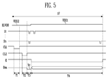
- FIG. 5 is a waveform diagram illustrating a driving method according to still another embodiment of the present invention.
- FIG. 5 detailed descriptions of components that are substantially identical to those of FIG. 4 will be omitted.
- the voltage of the first power source ELVDD is changed. That is, the first power source ELVDD is set to a first voltage VDD1 during the fourth period T4 in which the pixels 142 emit light, and is set to a second voltage VDD2 lower than the first voltage VDD1 during the first to third periods T1 to T3 in which the pixels 142 do not emit light.
- the second voltage VDD2 is set to a voltage higher than that of the initialization power source Vint so that the first transistor M1 is set in the on-bias state during the first period T1.
- the first power source ELVDD is set to the second voltage VDD2 during the first to third periods T1 to T3.
- the voltage of the first power source ELVDD is raised to the first voltage VDD1 during the fourth period T4.
- the first capacitor C1 is charged using the voltage charged in the second capacitor C2 during the second period T2.
- the voltage charged in the first capacitor C1 is set to a voltage lower than a desired voltage, and therefore, the organic light emitting diode OLED emits a small amount of light when the black is expressed (or represented).
- the voltage of the first power source ELVDD and the voltage at the first node N1 corresponding thereto are raised during the fourth period T4, so that it is possible to prevent the organic light emitting diode OLED from emitting a small amount of light when the black is expressed (or represented).
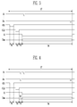
- FIG. 6 is a diagram illustrating an embodiment of a driving frequency in 3D driving.
- the organic light emitting display receives a data signal during an emission period. That is, the pixels 142 store a voltage corresponding to the right (or left) data signal during a period in which an image corresponding to the left (or right) data signal.
- a 3D image can be implemented at a driving frequency of 120Hz.
- RD represents a right data signal
- LD represents a left data signal.
- R represents emission corresponding to the right data signal
- L represents emission corresponding to the left data signal.
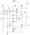
- FIG. 7 is a circuit diagram illustrating a pixel according to a second embodiment of the present invention.
- components that are substantially identical to those of FIG. 2 are designated by like reference numerals, and their detailed descriptions will be omitted.
- the pixel 142 includes a pixel circuit 200 and the organic light emitting diode OLED.
- the pixel circuit 200 includes the first driver 146 for storing the current data signal, and a second driver 202 for controlling an amount of the current supplied to the organic light emitting diode OLED, corresponding to the previous data signal.
- the second driver 202 includes a fourth transistor M4' coupled between the anode electrode of the organic light emitting diode OLED and the initialization power source Vint.
- a gate electrode of the fourth transistor M4' is coupled to the second control line CL2.
- the fourth transistor M4' is turned on when the second control signal is supplied to the second control line CL2, to supply the voltage of the initialization power source Vint to the anode electrode of the organic light emitting diode OLED.
- FIG. 8 is a circuit diagram illustrating a pixel according to a third embodiment of the present invention.
- components that are substantially identical to those of FIG. 2 are designated by like reference numerals, and their detailed descriptions will be omitted.
- the pixel 142 includes a pixel circuit 210 and the organic light emitting diode OLED.
- the pixel circuit 210 includes the first driver 146 for storing the current data signal, and a second driver 212 for controlling an amount of the current supplied to the organic light emitting diode OLED, corresponding to the previous data signal.
- the second driver 212 includes a photodiode PD coupled in parallel to the first capacitor C1 between the first power source ELVDD and the first node N1.
- the photodiode PD controls an amount of current supplied from the first power source ELVDD to the first node N1, i.e., the voltage at the first node N1, corresponding to the brightness of the organic light emitting diode OLED.
- the photodiode PD controls the voltage at the first node N1 so that the degradation of the organic light emitting diode OLED can be compensated for.
- the photodiode PD controls an amount of current flowing from the first power source ELVDD to the first node N1, i.e., an increment of the voltage at the first node N1, in proportion to the luminance of the organic light emitting diode OLED.
- the photodiode PD controls the voltage at the first node N1 to be increased as the luminance of the organic light emitting diode OLED increases.
- the organic light emitting diode OLED As the organic light emitting diode OLED is degraded, the organic light emitting diode OLED generates light with a low luminance, corresponding to the same gray level. Thus, the voltage at the first node N1 is changed by the photodiode PD, corresponding to the degradation of the organic light emitting diode OLED. That is, although a data signal with the same gray level is supplied, an increment of the voltage at the first node N1 is changed by the photodiode PD.
- the increment of the voltage at the first node N1 when the organic light emitting diode OLED is degraded is set lower by a first voltage V1 than that of the voltage at the first node N1 when the organic light emitting diode OLED is not degraded. That is, in the described embodiment of the present invention, the increment of the voltage at the first node N1 is set low as the organic light emitting diode OLED is degraded, and accordingly, it is possible to compensate for a decrease in luminance, caused by the degradation of the organic light emitting diode OLED.
- an amount of current supplied to the organic light emitting diode OLED may be represented as shown in Equation 1.
- I oled 1 2 ⁇ C ox W L ELVDD ⁇ V N 1 ⁇ V th 2
- I oled 1 2 ⁇ C ox W L ELVDD ⁇ C 2 Vdata + C 1 V int C 2 + C 1 ⁇ ⁇ V PD 2
- Equation 1 ⁇ denotes the mobility of the first transistor M1
- C ox denotes the gate capacitance of the first transistor
- V th denotes the threshold voltage of the first transistor M1
- W and L denote the channel width/length ratio of the first transistor M1.
- Vdata denotes the voltage of the data signal
- ⁇ V PD denotes a variation in voltage, caused by the photodiode PD.
- the operating process of the pixel 142 according to this embodiment, except that the photodiode PD is added so that the degradation of the organic light emitting diode OLED is compensated for, is substantially identical to that of the pixel in the first embodiment shown in FIG. 2 .
- the pixel 142 according to this embodiment can be driven with the driving waveforms shown in FIGS. 3 to 5 .
- FIG. 10 is a circuit diagram illustrating a pixel according to a fourth embodiment of the present invention.
- components that are substantially identical to those of FIG. 7 are designated by like reference numerals, and their detailed descriptions will be omitted.
- the pixel 142 includes a pixel circuit 220 and the organic light emitting diode OLED.
- the pixel circuit 220 includes the first driver 146 for storing the current data signal, and a second driver 222 for controlling an amount of the current supplied to the organic light emitting diode OLED, corresponding to the previous data signal.
- the second driver 222 includes a photodiode PD coupled in parallel to the first capacitor C1 between the first power source ELVDD and the first node N1.
- the photodiode PD controls an amount of current supplied from the first power source ELVDD to the first node N1, i.e., the voltage at the first node N1, corresponding to the brightness of the organic light emitting diode OLED.
- the photodiode PD controls the voltage at the first node N1 so that the degradation of the organic light emitting diode OLED can be compensated for.
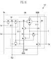
- FIG. 11 is a circuit diagram illustrating a pixel according to a fifth embodiment of the present invention.
- components that are substantially identical to those of FIG. 7 are designated by like reference numerals, and their detailed descriptions will be omitted.
- the pixel 142 includes a pixel circuit 230 and the organic light emitting diode OLED.
- the pixel circuit 230 includes the first driver 146 for storing the current data signal, and a second driver 232 for controlling an amount of the current supplied to the organic light emitting diode OLED, corresponding to the previous data signal.
- the second driver 232 includes a third capacitor C3 coupled between the second node N2 and the anode electrode of the organic light emitting diode OLED.
- the third capacitor C3 controls the voltage at the second node N2, corresponding to the voltage at the anode electrode of the organic light emitting diode OLED.
- the third capacitor C3 controls the voltage at the second node N2 so that the degradation of the organic light emitting diode OLED is compensated for.
- the pixel 142 according to this embodiment can be driven with any one of the driving waveforms shown in FIGS. 3 to 5 .
- the emission control signal is supplied to the emission control line E during the first to third periods T1 to T3, and the emission control signal is not supplied to the emission control line E during the fourth period T4.
- the eighth and ninth transistors M8 and M9 are turned off.
- the first transistor M1 and the organic light emitting diode OLED are electrically decoupled from each other, and accordingly, the organic light emitting diode OLED is set in the non-emission state during the first to third periods T1 to T3.
- the ninth transistor M9 is turned off, the anode electrode of the organic light emitting diode OLED is set to a voltage (e.g., a predetermined voltage) Voled.
- the first control signal is supplied to the first control line CL1 during the first period T1 so that the sixth and seventh transistors M6 and M7 are turned on.
- the voltage of the initialization power source Vint is supplied to the first node N1.
- the seventh transistor M7 is turned on, the voltage of the first power source ELVDD is supplied to the second node N2. In this case, the first transistor M1 is initialized in an on-bias state.
- the second control signal is supplied to the second control line CL2 during the second period T2.
- the fifth transistor M5 When the fifth transistor M5 is turned on, the first transistor M1 is diode-coupled.
- the third transistor M3 is turned on, the voltage of the previous data signal stored in the second capacitor C2 is supplied to the second node N2.
- the fourth transistor M4' When the fourth transistor M4' is turned on, the voltage Voled at the anode electrode of the organic light emitting diode OLED is dropped to the voltage of the initialization power source Vint. In this case, the voltage at the second node N2 is dropped, corresponding to a decrement of the voltage at the anode electrode of the organic light emitting diode OLED, by coupling of the third capacitor C3.
- the first transistor M1 When the voltage of the previous data signal is supplied to the second node N2, the first transistor M1 is turned on. When the first transistor M1 is turned on, the voltage applied to the second node N2 is supplied to the first node N1 via the diode-coupled first transistor M1. In this case, the first capacitor C1 stores a voltage corresponding to the previous data signal, the threshold voltage of the first transistor M1 and the degradation of the organic light emitting diode OLED.
- Voled denotes the voltage at the anode electrode of the organic light emitting diode OLED, applied during the first period T1.
- the voltage at the anode electrode of the organic light emitting diode OLED during the second period T2 is dropped from the voltage Voled applied during the first period T1 to the voltage of the initialization power source Vint.
- the variation ( ⁇ Voled) in the voltage at the anode electrode of the organic light emitting diode OLED is determined by the degradation of the organic light emitting diode OLED.
- the resistance of the organic light emitting diode OLED is increased. Accordingly, as the organic light emitting diode OLED is degraded, the variation ( ⁇ Voled) in the voltage at the anode electrode of the organic light emitting diode OLED is increased.
- the resistance of the organic light emitting diode OLED is increased corresponding to the degradation of the organic light emitting diode OLED.
- the resistance of the organic light emitting diode OLED is increased, the voltage Voled at the anode electrode of the organic light emitting diode OLED, which is applied during the first period T1, is increased.
- a decrement of the voltage at the second node N2 is increased, and accordingly, the degradation of the organic light emitting diode OLED can be compensated for.
- the voltage at the second node N2 is dropped, the voltage at the first node N1 is also dropped. Accordingly, as the organic light emitting diode OLED is degraded, an amount of the current supplied to the organic light emitting diode OLED is increased, thereby compensating for the degradation of the organic light emitting diode OLED.
- the supply of the emission control signal to the emission control line E is maintained during the third period T3.
- the supply of the emission control signal to the emission control line En is stopped during the fourth period T4, so that the eighth and ninth transistors M8 and M9 are turned on.
- the eighth transistor M8 is turned on, the first power source ELVDD and the second node N2 are electrically coupled to each other.
- the ninth transistor M9 is turned on, the fourth node N4 and the anode electrode of the organic light emitting diode OLED are electrically connected to each other.
- the first transistor M1 controls an amount of the current flowing from the first power source ELVDD to the second power source ELVSS via the organic light emitting diode OLED, corresponding to the voltage applied to the first node N1.
- the organic light emitting diode OLED generates light (e.g., light with a predetermined luminance) corresponding to an amount of current supplied thereto.
- the scan signal is progressively supplied to the scan lines S1 to Sn during the fourth period T4.
- the second transistor M2 included in each pixel 142 is turned on for each horizontal line.
- the current data signal from a data line (any one of D1 to Dm) is supplied to the third node N3 included in each pixel 142.
- the second capacitor C2 charges a voltage corresponding to the current data signal.
- FIG. 12 is a circuit diagram illustrating a pixel according to a sixth embodiment of the present invention.
- components that are substantially identical to those of FIG. 11 are designated by like reference numerals, and their detailed descriptions will be omitted.
- the pixel includes a pixel circuit 240 and the organic light emitting diode OLED.
- the pixel circuit 240 includes the first driver 146 for storing the current data signal, and a second driver 242 for controlling an amount of the current supplied to the organic light emitting diode OLED, corresponding to the previous data signal.
- the second driver 242 includes a fourth transistor M4" coupled between the second control line CL2 and the organic light emitting diode OLED.
- a gate electrode of the fourth transistor M4" is coupled to the second control line CL2. That is, the fourth transistor M4" is diode-coupled.
- the fourth transistor M4" allows the voltage at the anode electrode of the organic light emitting diode OLED to be dropped to approximately the voltage of the second control signal when the second control signal is supplied to the second control line CL2.
- the operating process of the pixel according to this embodiment except that the voltage Voled at the anode electrode of the organic light emitting diode OLED is dropped to the voltage of the second control signal other than that of the initialization power source Vint, is substantially identical to that of the pixel according to the fifth embodiment shown in FIG. 11 . Therefore, its detailed description will be omitted.
- the transistors are shown as PMOS transistors for convenience of illustration, the present invention is not limited thereto.
- the transistors may be formed as NMOS transistors.
- the organic light emitting diode OLED may generate red, green and blue light, corresponding to an amount of current supplied from the driving transistor, or may generate white light, corresponding to the amount of the current supplied from the driving transistor.
- a color image is implemented using a separate color filter or the like.
- an organic light emitting display includes a plurality of pixels arranged in a matrix form at crossing regions of a plurality of data lines, a plurality of scan lines and a plurality of power lines.
- Each pixel generally includes an organic light emitting diode, two or more transistors including a driving transistor, and one or more capacitors.
- the organic light emitting display includes four frames during a period of 16.6 ms.
- a left image is displayed in a first frame among the four frames, and a right image is displayed in a third frame among the four frames.
- a black image is displayed in second and fourth frames among the four frames.
- a left lens receives light during the first frame, and a right lens receives light during the third frame.
- a user wearing the shutter glasses recognizes, as a 3D image, an image supplied through the shutter glasses.
- the left and right lenses switch from either receiving light to not receiving light or from not receiving light to receiving light while the black image is being displayed during the second and fourth frames, and thus it is possible to prevent the occurrence of a crosstalk phenomenon.
- the four frames are included in the period of 16.6 ms, and accordingly, the organic light emitting display is driven at a driving frequency of 240Hz.
- the organic light emitting display is driven at a high frequency, the power consumption of the organic light emitting display is increased, and the stability of the organic light emitting display is lowered. Further, the manufacturing cost of the organic light emitting display is increased. Since the black image is displayed during the second and fourth frames, the peak current for expressing a gray scale is increased, and accordingly, the lifespan of the organic light emitting diode is lowered.
- the pixels emit light, and concurrently (e.g., simultaneously), the data signal can be charged. Accordingly, the organic light emitting display is driven at a low frequency, thereby implementing a 3D image. Further, the driving transistor included in each pixel is initialized in an on-bias state before the data signal is supplied, thereby displaying a uniform image.
Landscapes
- Engineering & Computer Science (AREA)
- Physics & Mathematics (AREA)
- Computer Hardware Design (AREA)
- General Physics & Mathematics (AREA)
- Theoretical Computer Science (AREA)
- Control Of Indicators Other Than Cathode Ray Tubes (AREA)
- Control Of El Displays (AREA)
- Electroluminescent Light Sources (AREA)
Applications Claiming Priority (4)
| Application Number | Priority Date | Filing Date | Title |
|---|---|---|---|
| KR20130005453 | 2013-01-17 | ||
| KR20130005454 | 2013-01-17 | ||
| KR1020130075336A KR102098143B1 (ko) | 2013-01-17 | 2013-06-28 | 화소 및 이를 이용한 유기전계발광 표시장치 |
| EP14151419.0A EP2757548B1 (fr) | 2013-01-17 | 2014-01-16 | Pixel et affichage électroluminescent organique l'utilisant |
Related Parent Applications (2)
| Application Number | Title | Priority Date | Filing Date |
|---|---|---|---|
| EP14151419.0A Division EP2757548B1 (fr) | 2013-01-17 | 2014-01-16 | Pixel et affichage électroluminescent organique l'utilisant |
| EP14151419.0A Division-Into EP2757548B1 (fr) | 2013-01-17 | 2014-01-16 | Pixel et affichage électroluminescent organique l'utilisant |
Publications (2)
| Publication Number | Publication Date |
|---|---|
| EP3093835A1 true EP3093835A1 (fr) | 2016-11-16 |
| EP3093835B1 EP3093835B1 (fr) | 2018-03-14 |
Family
ID=49920288
Family Applications (2)
| Application Number | Title | Priority Date | Filing Date |
|---|---|---|---|
| EP14151419.0A Active EP2757548B1 (fr) | 2013-01-17 | 2014-01-16 | Pixel et affichage électroluminescent organique l'utilisant |
| EP16176868.4A Active EP3093835B1 (fr) | 2013-01-17 | 2014-01-16 | Pixel et affichage électroluminescent organique l'utilisant |
Family Applications Before (1)
| Application Number | Title | Priority Date | Filing Date |
|---|---|---|---|
| EP14151419.0A Active EP2757548B1 (fr) | 2013-01-17 | 2014-01-16 | Pixel et affichage électroluminescent organique l'utilisant |
Country Status (4)
| Country | Link |
|---|---|
| US (1) | US9576535B2 (fr) |
| EP (2) | EP2757548B1 (fr) |
| JP (1) | JP6381916B2 (fr) |
| CN (1) | CN103943063B (fr) |
Families Citing this family (37)
| Publication number | Priority date | Publication date | Assignee | Title |
|---|---|---|---|---|
| KR101893167B1 (ko) | 2012-03-23 | 2018-10-05 | 삼성디스플레이 주식회사 | 화소 회로, 이의 구동 방법 및 유기 발광 표시 장치 |
| KR102206602B1 (ko) | 2014-07-14 | 2021-01-25 | 삼성디스플레이 주식회사 | 화소 및 이를 이용한 유기전계발광 표시장치 |
| KR102150039B1 (ko) | 2014-07-14 | 2020-09-01 | 삼성디스플레이 주식회사 | 화소 및 이를 이용한 유기전계발광 표시장치 |
| KR102249055B1 (ko) | 2014-09-03 | 2021-05-10 | 삼성디스플레이 주식회사 | 열화 보상 픽셀 회로 및 이를 포함하는 유기 발광 다이오드 표시 장치 |
| TWI533278B (zh) * | 2014-10-31 | 2016-05-11 | 友達光電股份有限公司 | 畫素結構及其驅動方法 |
| CN104485072B (zh) * | 2014-12-22 | 2017-03-08 | 昆山国显光电有限公司 | 像素电路及其驱动方法和有源矩阵有机发光显示器 |
| KR102265368B1 (ko) * | 2015-01-13 | 2021-06-15 | 삼성디스플레이 주식회사 | 화소, 이를 포함하는 표시 장치 및 그 구동방법 |
| CN104700780B (zh) * | 2015-03-31 | 2017-12-05 | 京东方科技集团股份有限公司 | 一种像素电路的驱动方法 |
| KR102524459B1 (ko) | 2015-08-27 | 2023-04-25 | 삼성디스플레이 주식회사 | 화소 및 그의 구동방법 |
| CN105427806B (zh) * | 2016-01-06 | 2018-10-23 | 京东方科技集团股份有限公司 | 像素电路、显示基板及显示装置、驱动显示基板的方法 |
| CN107919089B (zh) * | 2016-10-09 | 2019-11-22 | 上海和辉光电有限公司 | 一种像素阵列及其虚拟现实中的显示电路 |
| KR102697200B1 (ko) * | 2016-12-20 | 2024-08-20 | 엘지디스플레이 주식회사 | 게이트 구동회로 및 이를 포함하는 표시 장치 |
| CN106782331B (zh) * | 2016-12-27 | 2023-07-18 | 京东方科技集团股份有限公司 | 一种像素电路、其驱动方法、显示面板及显示装置 |
| CN110164370B (zh) * | 2018-05-14 | 2021-08-10 | 京东方科技集团股份有限公司 | 一种像素电路、补偿组件、显示装置及其驱动方法 |
| CN118675469A (zh) * | 2018-09-13 | 2024-09-20 | 京东方科技集团股份有限公司 | 像素电路及其驱动方法、显示装置 |
| JP7272787B2 (ja) * | 2018-12-20 | 2023-05-12 | エルジー ディスプレイ カンパニー リミテッド | 発光表示装置 |
| CN113348498A (zh) * | 2019-04-08 | 2021-09-03 | 深圳市柔宇科技股份有限公司 | 显示面板及显示装置 |
| CN110070831B (zh) * | 2019-04-19 | 2021-08-06 | 深圳市华星光电半导体显示技术有限公司 | 像素驱动电路及显示面板 |
| TWI732254B (zh) * | 2019-07-30 | 2021-07-01 | 友達光電股份有限公司 | 顯示裝置及畫素電路 |
| CN110491338B (zh) * | 2019-08-28 | 2021-02-02 | 京东方科技集团股份有限公司 | 像素电路及其驱动方法、发光控制电路及方法、显示装置 |
| KR102636598B1 (ko) * | 2019-12-13 | 2024-02-13 | 엘지디스플레이 주식회사 | 화소 구동 회로를 포함한 전계발광 표시장치 |
| CN111312174B (zh) * | 2020-02-25 | 2021-05-25 | 厦门天马微电子有限公司 | 有机发光显示装置的驱动方法及有机发光显示装置 |
| KR102742215B1 (ko) | 2020-04-06 | 2024-12-16 | 삼성디스플레이 주식회사 | 표시 장치 |
| CN112071269A (zh) * | 2020-09-24 | 2020-12-11 | 京东方科技集团股份有限公司 | 像素单元驱动电路、驱动方法、显示面板及显示装置 |
| US12159582B2 (en) * | 2021-01-19 | 2024-12-03 | Sharp Kabushiki Kaisha | Pixel circuit, display device, and method for driving same |
| CN112706609A (zh) | 2021-01-22 | 2021-04-27 | 国网安徽省电力有限公司淮北供电公司 | 一种电力灾害故障应急检修装置 |
| CN112992055B (zh) * | 2021-04-27 | 2021-07-27 | 武汉华星光电半导体显示技术有限公司 | 像素电路及显示面板 |
| KR20230016775A (ko) * | 2021-07-26 | 2023-02-03 | 삼성디스플레이 주식회사 | 표시 장치 |
| CN113643669B (zh) * | 2021-08-03 | 2022-09-27 | 武汉华星光电技术有限公司 | Goa电路及显示面板 |
| KR102877105B1 (ko) * | 2021-08-24 | 2025-10-28 | 삼성디스플레이 주식회사 | 리페어 픽셀 및 이를 포함하는 표시 장치 |
| KR102863273B1 (ko) * | 2021-12-27 | 2025-09-22 | 엘지디스플레이 주식회사 | 표시 장치 |
| CN115311984B (zh) * | 2022-08-25 | 2025-02-25 | 厦门天马显示科技有限公司 | 显示面板和显示装置 |
| KR20240055281A (ko) * | 2022-10-20 | 2024-04-29 | 엘지디스플레이 주식회사 | 표시 장치 |
| KR20240108906A (ko) * | 2022-12-30 | 2024-07-10 | 엘지디스플레이 주식회사 | 표시 장치 및 그 구동 방법 |
| CN116030761B (zh) * | 2023-02-13 | 2024-05-31 | 武汉天马微电子有限公司 | 一种像素电路、显示面板及显示装置 |
| CN116645922A (zh) * | 2023-06-06 | 2023-08-25 | 京东方科技集团股份有限公司 | 像素驱动电路及驱动方法、显示基板、显示装置 |
| KR20250085021A (ko) * | 2023-12-04 | 2025-06-12 | 삼성디스플레이 주식회사 | 화소 |
Citations (7)
| Publication number | Priority date | Publication date | Assignee | Title |
|---|---|---|---|---|
| US20080243498A1 (en) | 2007-03-30 | 2008-10-02 | Verizon Data Services, Inc. | Method and system for providing interactive speech recognition using speaker data |
| US20090243498A1 (en) * | 2003-08-08 | 2009-10-01 | Childs Mark J | Electroluminescent display devices |
| EP2146337A1 (fr) | 2008-07-18 | 2010-01-20 | Samsung Mobile Display Co., Ltd. | Pixel et dispositif d'affichage électroluminescent organique l'utilisant |
| US20110090200A1 (en) | 2009-10-19 | 2011-04-21 | Sang-Moo Choi | Organic light emitting display device and driving method thereof |
| US20110279484A1 (en) | 2010-05-13 | 2011-11-17 | Han Sang-Myeon | Organic light emitting display device and driving method thereof |
| US20120113077A1 (en) | 2010-11-05 | 2012-05-10 | Chul-Kyu Kang | Pixel and organic light emitting display using the same |
| EP2463849A1 (fr) | 2010-12-10 | 2012-06-13 | Samsung Mobile Display Co., Ltd. | Pixel, dispositif d'affichage l'utilisant et son procédé de commande |
Family Cites Families (20)
| Publication number | Priority date | Publication date | Assignee | Title |
|---|---|---|---|---|
| KR100560780B1 (ko) | 2003-07-07 | 2006-03-13 | 삼성에스디아이 주식회사 | 유기전계 발광표시장치의 화소회로 및 그의 구동방법 |
| KR100741973B1 (ko) | 2005-08-12 | 2007-07-23 | 삼성에스디아이 주식회사 | 유기 전계발광 표시장치 |
| JP4887203B2 (ja) | 2006-11-14 | 2012-02-29 | 三星モバイルディスプレイ株式會社 | 画素、有機電界発光表示装置、および有機電界発光表示装置の駆動方法 |
| KR100815756B1 (ko) | 2006-11-14 | 2008-03-20 | 삼성에스디아이 주식회사 | 화소 및 이를 이용한 유기전계발광 표시장치 및 그의구동방법 |
| CN101542572A (zh) | 2006-11-28 | 2009-09-23 | 皇家飞利浦电子股份有限公司 | 具有光学反馈的有源矩阵显示器件及其驱动方法 |
| WO2008065583A1 (fr) | 2006-11-28 | 2008-06-05 | Koninklijke Philips Electronics N.V. | Dispositif d'affichage électroluminescent à matrice active et procédé de commande de celui-ci |
| KR100836432B1 (ko) | 2007-02-05 | 2008-06-09 | 삼성에스디아이 주식회사 | 유기 전계 발광표시장치 및 그 구동방법 |
| KR100865394B1 (ko) * | 2007-03-02 | 2008-10-24 | 삼성에스디아이 주식회사 | 유기 전계 발광 표시 장치 |
| KR100865396B1 (ko) | 2007-03-02 | 2008-10-24 | 삼성에스디아이 주식회사 | 유기 전계 발광 표시 장치 |
| KR100873076B1 (ko) | 2007-03-14 | 2008-12-09 | 삼성모바일디스플레이주식회사 | 화소 및 이를 이용한 유기전계발광 표시장치 및 그의구동방법 |
| KR100873078B1 (ko) | 2007-04-10 | 2008-12-09 | 삼성모바일디스플레이주식회사 | 화소 및 이를 이용한 유기전계발광 표시장치 및 그의구동방법 |
| KR100911969B1 (ko) | 2007-12-06 | 2009-08-13 | 삼성모바일디스플레이주식회사 | 화소 및 이를 이용한 유기전계발광 표시장치 |
| KR100952111B1 (ko) | 2008-03-31 | 2010-04-13 | 한양대학교 산학협력단 | 광 감지 기능을 가지는 유기발광다이오드(oled)의 화소회로, 이를 포함하는 디스플레이 장치 |
| KR101056240B1 (ko) * | 2009-03-02 | 2011-08-11 | 삼성모바일디스플레이주식회사 | 유기전계발광 표시장치 |
| JP2010266492A (ja) * | 2009-05-12 | 2010-11-25 | Sony Corp | 画素回路、表示装置、画素回路の駆動方法 |
| KR101022118B1 (ko) | 2009-09-02 | 2011-03-17 | 삼성모바일디스플레이주식회사 | 광 감지회로 및 그 구동방법과 이를 구비한 터치 스크린 패널 |
| KR101097325B1 (ko) * | 2009-12-31 | 2011-12-23 | 삼성모바일디스플레이주식회사 | 화소 회로 및 유기 전계 발광 표시 장치 |
| KR101681097B1 (ko) * | 2010-07-27 | 2016-12-02 | 삼성디스플레이 주식회사 | 화소 및 이를 이용한 유기전계발광 표시장치 |
| KR101791664B1 (ko) * | 2010-10-28 | 2017-11-21 | 삼성디스플레이 주식회사 | 유기전계발광 표시장치 |
| KR20130135506A (ko) | 2012-06-01 | 2013-12-11 | 삼성디스플레이 주식회사 | 화소 및 이를 이용한 유기전계발광 표시장치 |
-
2014
- 2014-01-06 US US14/148,667 patent/US9576535B2/en active Active
- 2014-01-16 JP JP2014005707A patent/JP6381916B2/ja active Active
- 2014-01-16 EP EP14151419.0A patent/EP2757548B1/fr active Active
- 2014-01-16 EP EP16176868.4A patent/EP3093835B1/fr active Active
- 2014-01-17 CN CN201410022760.2A patent/CN103943063B/zh active Active
Patent Citations (7)
| Publication number | Priority date | Publication date | Assignee | Title |
|---|---|---|---|---|
| US20090243498A1 (en) * | 2003-08-08 | 2009-10-01 | Childs Mark J | Electroluminescent display devices |
| US20080243498A1 (en) | 2007-03-30 | 2008-10-02 | Verizon Data Services, Inc. | Method and system for providing interactive speech recognition using speaker data |
| EP2146337A1 (fr) | 2008-07-18 | 2010-01-20 | Samsung Mobile Display Co., Ltd. | Pixel et dispositif d'affichage électroluminescent organique l'utilisant |
| US20110090200A1 (en) | 2009-10-19 | 2011-04-21 | Sang-Moo Choi | Organic light emitting display device and driving method thereof |
| US20110279484A1 (en) | 2010-05-13 | 2011-11-17 | Han Sang-Myeon | Organic light emitting display device and driving method thereof |
| US20120113077A1 (en) | 2010-11-05 | 2012-05-10 | Chul-Kyu Kang | Pixel and organic light emitting display using the same |
| EP2463849A1 (fr) | 2010-12-10 | 2012-06-13 | Samsung Mobile Display Co., Ltd. | Pixel, dispositif d'affichage l'utilisant et son procédé de commande |
Also Published As
| Publication number | Publication date |
|---|---|
| EP3093835B1 (fr) | 2018-03-14 |
| EP2757548A2 (fr) | 2014-07-23 |
| CN103943063B (zh) | 2018-05-29 |
| US20140198085A1 (en) | 2014-07-17 |
| US9576535B2 (en) | 2017-02-21 |
| CN103943063A (zh) | 2014-07-23 |
| EP2757548A3 (fr) | 2014-08-13 |
| JP2014137601A (ja) | 2014-07-28 |
| JP6381916B2 (ja) | 2018-08-29 |
| EP2757548B1 (fr) | 2016-08-17 |
Similar Documents
| Publication | Publication Date | Title |
|---|---|---|
| EP3093835B1 (fr) | Pixel et affichage électroluminescent organique l'utilisant | |
| US9460658B2 (en) | Pixel and organic light emitting display device using the same | |
| KR101783898B1 (ko) | 화소 및 이를 이용한 유기전계발광 표시장치 | |
| KR101082234B1 (ko) | 유기전계발광 표시장치 및 그의 구동방법 | |
| US9269303B2 (en) | Organic light emitting display device and method of driving the same | |
| KR101073281B1 (ko) | 유기전계발광 표시장치 및 그의 구동방법 | |
| KR102141238B1 (ko) | 화소 및 이를 이용한 유기전계발광 표시장치 | |
| US9064458B2 (en) | Organic light emitting display and driving method thereof | |
| KR100592646B1 (ko) | 발광 표시장치 및 그의 구동방법 | |
| KR101674479B1 (ko) | 유기전계발광 표시장치 | |
| KR20140081262A (ko) | 화소 및 이를 이용한 유기전계발광 표시장치 | |
| US9396681B2 (en) | Pixel circuit and organic light emitting display device using the same | |
| EP2284825A1 (fr) | Affichage électroluminescent organique et procédé de commande correspondant | |
| US20140168180A1 (en) | Pixel and organic light emitting display device using the same | |
| KR101210029B1 (ko) | 유기전계발광 표시장치 | |
| KR102098143B1 (ko) | 화소 및 이를 이용한 유기전계발광 표시장치 | |
| US20130321376A1 (en) | Pixel and organic light emitting display device using the same | |
| KR102042192B1 (ko) | 화소 및 이를 이용한 유기전계발광 표시장치 | |
| KR20140132504A (ko) | 화소 및 이를 이용한 유기전계발광 표시장치 | |
| KR101122894B1 (ko) | 유기 전계발광 표시장치 및 그의 구동방법 | |
| KR20140134048A (ko) | 화소 및 이를 이용한 유기전계발광 표시장치 | |
| KR20160008705A (ko) | 화소 및 이를 이용한 유기전계발광 표시장치 | |
| KR101683215B1 (ko) | 유기전계발광 표시장치 및 그의 구동방법 | |
| KR20150109524A (ko) | 유기전계발광 표시장치 및 그의 구동방법 |
Legal Events
| Date | Code | Title | Description |
|---|---|---|---|
| PUAI | Public reference made under article 153(3) epc to a published international application that has entered the european phase |
Free format text: ORIGINAL CODE: 0009012 |
|
| AC | Divisional application: reference to earlier application |
Ref document number: 2757548 Country of ref document: EP Kind code of ref document: P |
|
| AK | Designated contracting states |
Kind code of ref document: A1 Designated state(s): AL AT BE BG CH CY CZ DE DK EE ES FI FR GB GR HR HU IE IS IT LI LT LU LV MC MK MT NL NO PL PT RO RS SE SI SK SM TR |
|
| STAA | Information on the status of an ep patent application or granted ep patent |
Free format text: STATUS: REQUEST FOR EXAMINATION WAS MADE |
|
| 17P | Request for examination filed |
Effective date: 20170516 |
|
| RBV | Designated contracting states (corrected) |
Designated state(s): AL AT BE BG CH CY CZ DE DK EE ES FI FR GB GR HR HU IE IS IT LI LT LU LV MC MK MT NL NO PL PT RO RS SE SI SK SM TR |
|
| STAA | Information on the status of an ep patent application or granted ep patent |
Free format text: STATUS: EXAMINATION IS IN PROGRESS |
|
| 17Q | First examination report despatched |
Effective date: 20170707 |
|
| GRAP | Despatch of communication of intention to grant a patent |
Free format text: ORIGINAL CODE: EPIDOSNIGR1 |
|
| STAA | Information on the status of an ep patent application or granted ep patent |
Free format text: STATUS: GRANT OF PATENT IS INTENDED |
|
| INTG | Intention to grant announced |
Effective date: 20171011 |
|
| GRAS | Grant fee paid |
Free format text: ORIGINAL CODE: EPIDOSNIGR3 |
|
| GRAA | (expected) grant |
Free format text: ORIGINAL CODE: 0009210 |
|
| STAA | Information on the status of an ep patent application or granted ep patent |
Free format text: STATUS: THE PATENT HAS BEEN GRANTED |
|
| AC | Divisional application: reference to earlier application |
Ref document number: 2757548 Country of ref document: EP Kind code of ref document: P |
|
| AK | Designated contracting states |
Kind code of ref document: B1 Designated state(s): AL AT BE BG CH CY CZ DE DK EE ES FI FR GB GR HR HU IE IS IT LI LT LU LV MC MK MT NL NO PL PT RO RS SE SI SK SM TR |
|
| REG | Reference to a national code |
Ref country code: GB Ref legal event code: FG4D |
|
| REG | Reference to a national code |
Ref country code: CH Ref legal event code: EP Ref country code: AT Ref legal event code: REF Ref document number: 979583 Country of ref document: AT Kind code of ref document: T Effective date: 20180315 |
|
| REG | Reference to a national code |
Ref country code: IE Ref legal event code: FG4D |
|
| REG | Reference to a national code |
Ref country code: DE Ref legal event code: R096 Ref document number: 602014022478 Country of ref document: DE |
|
| REG | Reference to a national code |
Ref country code: NL Ref legal event code: MP Effective date: 20180314 |
|
| REG | Reference to a national code |
Ref country code: LT Ref legal event code: MG4D |
|
| PG25 | Lapsed in a contracting state [announced via postgrant information from national office to epo] |
Ref country code: NO Free format text: LAPSE BECAUSE OF FAILURE TO SUBMIT A TRANSLATION OF THE DESCRIPTION OR TO PAY THE FEE WITHIN THE PRESCRIBED TIME-LIMIT Effective date: 20180614 Ref country code: FI Free format text: LAPSE BECAUSE OF FAILURE TO SUBMIT A TRANSLATION OF THE DESCRIPTION OR TO PAY THE FEE WITHIN THE PRESCRIBED TIME-LIMIT Effective date: 20180314 Ref country code: CY Free format text: LAPSE BECAUSE OF FAILURE TO SUBMIT A TRANSLATION OF THE DESCRIPTION OR TO PAY THE FEE WITHIN THE PRESCRIBED TIME-LIMIT Effective date: 20180314 Ref country code: LT Free format text: LAPSE BECAUSE OF FAILURE TO SUBMIT A TRANSLATION OF THE DESCRIPTION OR TO PAY THE FEE WITHIN THE PRESCRIBED TIME-LIMIT Effective date: 20180314 Ref country code: HR Free format text: LAPSE BECAUSE OF FAILURE TO SUBMIT A TRANSLATION OF THE DESCRIPTION OR TO PAY THE FEE WITHIN THE PRESCRIBED TIME-LIMIT Effective date: 20180314 |
|
| REG | Reference to a national code |
Ref country code: AT Ref legal event code: MK05 Ref document number: 979583 Country of ref document: AT Kind code of ref document: T Effective date: 20180314 |
|
| PG25 | Lapsed in a contracting state [announced via postgrant information from national office to epo] |
Ref country code: RS Free format text: LAPSE BECAUSE OF FAILURE TO SUBMIT A TRANSLATION OF THE DESCRIPTION OR TO PAY THE FEE WITHIN THE PRESCRIBED TIME-LIMIT Effective date: 20180314 Ref country code: SE Free format text: LAPSE BECAUSE OF FAILURE TO SUBMIT A TRANSLATION OF THE DESCRIPTION OR TO PAY THE FEE WITHIN THE PRESCRIBED TIME-LIMIT Effective date: 20180314 Ref country code: BG Free format text: LAPSE BECAUSE OF FAILURE TO SUBMIT A TRANSLATION OF THE DESCRIPTION OR TO PAY THE FEE WITHIN THE PRESCRIBED TIME-LIMIT Effective date: 20180614 Ref country code: LV Free format text: LAPSE BECAUSE OF FAILURE TO SUBMIT A TRANSLATION OF THE DESCRIPTION OR TO PAY THE FEE WITHIN THE PRESCRIBED TIME-LIMIT Effective date: 20180314 Ref country code: GR Free format text: LAPSE BECAUSE OF FAILURE TO SUBMIT A TRANSLATION OF THE DESCRIPTION OR TO PAY THE FEE WITHIN THE PRESCRIBED TIME-LIMIT Effective date: 20180615 |
|
| PG25 | Lapsed in a contracting state [announced via postgrant information from national office to epo] |
Ref country code: ES Free format text: LAPSE BECAUSE OF FAILURE TO SUBMIT A TRANSLATION OF THE DESCRIPTION OR TO PAY THE FEE WITHIN THE PRESCRIBED TIME-LIMIT Effective date: 20180314 Ref country code: PL Free format text: LAPSE BECAUSE OF FAILURE TO SUBMIT A TRANSLATION OF THE DESCRIPTION OR TO PAY THE FEE WITHIN THE PRESCRIBED TIME-LIMIT Effective date: 20180314 Ref country code: EE Free format text: LAPSE BECAUSE OF FAILURE TO SUBMIT A TRANSLATION OF THE DESCRIPTION OR TO PAY THE FEE WITHIN THE PRESCRIBED TIME-LIMIT Effective date: 20180314 Ref country code: RO Free format text: LAPSE BECAUSE OF FAILURE TO SUBMIT A TRANSLATION OF THE DESCRIPTION OR TO PAY THE FEE WITHIN THE PRESCRIBED TIME-LIMIT Effective date: 20180314 Ref country code: NL Free format text: LAPSE BECAUSE OF FAILURE TO SUBMIT A TRANSLATION OF THE DESCRIPTION OR TO PAY THE FEE WITHIN THE PRESCRIBED TIME-LIMIT Effective date: 20180314 Ref country code: AL Free format text: LAPSE BECAUSE OF FAILURE TO SUBMIT A TRANSLATION OF THE DESCRIPTION OR TO PAY THE FEE WITHIN THE PRESCRIBED TIME-LIMIT Effective date: 20180314 |
|
| PG25 | Lapsed in a contracting state [announced via postgrant information from national office to epo] |
Ref country code: SK Free format text: LAPSE BECAUSE OF FAILURE TO SUBMIT A TRANSLATION OF THE DESCRIPTION OR TO PAY THE FEE WITHIN THE PRESCRIBED TIME-LIMIT Effective date: 20180314 Ref country code: AT Free format text: LAPSE BECAUSE OF FAILURE TO SUBMIT A TRANSLATION OF THE DESCRIPTION OR TO PAY THE FEE WITHIN THE PRESCRIBED TIME-LIMIT Effective date: 20180314 Ref country code: SM Free format text: LAPSE BECAUSE OF FAILURE TO SUBMIT A TRANSLATION OF THE DESCRIPTION OR TO PAY THE FEE WITHIN THE PRESCRIBED TIME-LIMIT Effective date: 20180314 Ref country code: CZ Free format text: LAPSE BECAUSE OF FAILURE TO SUBMIT A TRANSLATION OF THE DESCRIPTION OR TO PAY THE FEE WITHIN THE PRESCRIBED TIME-LIMIT Effective date: 20180314 |
|
| REG | Reference to a national code |
Ref country code: DE Ref legal event code: R097 Ref document number: 602014022478 Country of ref document: DE |
|
| PG25 | Lapsed in a contracting state [announced via postgrant information from national office to epo] |
Ref country code: PT Free format text: LAPSE BECAUSE OF FAILURE TO SUBMIT A TRANSLATION OF THE DESCRIPTION OR TO PAY THE FEE WITHIN THE PRESCRIBED TIME-LIMIT Effective date: 20180716 |
|
| PLBE | No opposition filed within time limit |
Free format text: ORIGINAL CODE: 0009261 |
|
| STAA | Information on the status of an ep patent application or granted ep patent |
Free format text: STATUS: NO OPPOSITION FILED WITHIN TIME LIMIT |
|
| PG25 | Lapsed in a contracting state [announced via postgrant information from national office to epo] |
Ref country code: DK Free format text: LAPSE BECAUSE OF FAILURE TO SUBMIT A TRANSLATION OF THE DESCRIPTION OR TO PAY THE FEE WITHIN THE PRESCRIBED TIME-LIMIT Effective date: 20180314 |
|
| 26N | No opposition filed |
Effective date: 20181217 |
|
| PG25 | Lapsed in a contracting state [announced via postgrant information from national office to epo] |
Ref country code: SI Free format text: LAPSE BECAUSE OF FAILURE TO SUBMIT A TRANSLATION OF THE DESCRIPTION OR TO PAY THE FEE WITHIN THE PRESCRIBED TIME-LIMIT Effective date: 20180314 Ref country code: IT Free format text: LAPSE BECAUSE OF FAILURE TO SUBMIT A TRANSLATION OF THE DESCRIPTION OR TO PAY THE FEE WITHIN THE PRESCRIBED TIME-LIMIT Effective date: 20180314 |
|
| PG25 | Lapsed in a contracting state [announced via postgrant information from national office to epo] |
Ref country code: MC Free format text: LAPSE BECAUSE OF FAILURE TO SUBMIT A TRANSLATION OF THE DESCRIPTION OR TO PAY THE FEE WITHIN THE PRESCRIBED TIME-LIMIT Effective date: 20180314 |
|
| REG | Reference to a national code |
Ref country code: CH Ref legal event code: PL |
|
| PG25 | Lapsed in a contracting state [announced via postgrant information from national office to epo] |
Ref country code: LU Free format text: LAPSE BECAUSE OF NON-PAYMENT OF DUE FEES Effective date: 20190116 |
|
| REG | Reference to a national code |
Ref country code: BE Ref legal event code: MM Effective date: 20190131 |
|
| REG | Reference to a national code |
Ref country code: IE Ref legal event code: MM4A |
|
| PG25 | Lapsed in a contracting state [announced via postgrant information from national office to epo] |
Ref country code: FR Free format text: LAPSE BECAUSE OF NON-PAYMENT OF DUE FEES Effective date: 20190131 |
|
| PG25 | Lapsed in a contracting state [announced via postgrant information from national office to epo] |
Ref country code: BE Free format text: LAPSE BECAUSE OF NON-PAYMENT OF DUE FEES Effective date: 20190131 |
|
| PG25 | Lapsed in a contracting state [announced via postgrant information from national office to epo] |
Ref country code: CH Free format text: LAPSE BECAUSE OF NON-PAYMENT OF DUE FEES Effective date: 20190131 Ref country code: LI Free format text: LAPSE BECAUSE OF NON-PAYMENT OF DUE FEES Effective date: 20190131 |
|
| PG25 | Lapsed in a contracting state [announced via postgrant information from national office to epo] |
Ref country code: IE Free format text: LAPSE BECAUSE OF NON-PAYMENT OF DUE FEES Effective date: 20190116 |
|
| PG25 | Lapsed in a contracting state [announced via postgrant information from national office to epo] |
Ref country code: TR Free format text: LAPSE BECAUSE OF FAILURE TO SUBMIT A TRANSLATION OF THE DESCRIPTION OR TO PAY THE FEE WITHIN THE PRESCRIBED TIME-LIMIT Effective date: 20180314 |
|
| PG25 | Lapsed in a contracting state [announced via postgrant information from national office to epo] |
Ref country code: MT Free format text: LAPSE BECAUSE OF NON-PAYMENT OF DUE FEES Effective date: 20190116 |
|
| PG25 | Lapsed in a contracting state [announced via postgrant information from national office to epo] |
Ref country code: IS Free format text: LAPSE BECAUSE OF FAILURE TO SUBMIT A TRANSLATION OF THE DESCRIPTION OR TO PAY THE FEE WITHIN THE PRESCRIBED TIME-LIMIT Effective date: 20180714 |
|
| PG25 | Lapsed in a contracting state [announced via postgrant information from national office to epo] |
Ref country code: HU Free format text: LAPSE BECAUSE OF FAILURE TO SUBMIT A TRANSLATION OF THE DESCRIPTION OR TO PAY THE FEE WITHIN THE PRESCRIBED TIME-LIMIT; INVALID AB INITIO Effective date: 20140116 |
|
| PG25 | Lapsed in a contracting state [announced via postgrant information from national office to epo] |
Ref country code: MK Free format text: LAPSE BECAUSE OF FAILURE TO SUBMIT A TRANSLATION OF THE DESCRIPTION OR TO PAY THE FEE WITHIN THE PRESCRIBED TIME-LIMIT Effective date: 20180314 |
|
| P01 | Opt-out of the competence of the unified patent court (upc) registered |
Effective date: 20230516 |
|
| PGFP | Annual fee paid to national office [announced via postgrant information from national office to epo] |
Ref country code: GB Payment date: 20251222 Year of fee payment: 13 |
|
| PGFP | Annual fee paid to national office [announced via postgrant information from national office to epo] |
Ref country code: DE Payment date: 20251222 Year of fee payment: 13 |