EP3093976B1 - Système de conversion d'énergie électrique - Google Patents
Système de conversion d'énergie électrique Download PDFInfo
- Publication number
- EP3093976B1 EP3093976B1 EP14876755.1A EP14876755A EP3093976B1 EP 3093976 B1 EP3093976 B1 EP 3093976B1 EP 14876755 A EP14876755 A EP 14876755A EP 3093976 B1 EP3093976 B1 EP 3093976B1
- Authority
- EP
- European Patent Office
- Prior art keywords
- voltage
- phase
- carrier signal
- stage
- capacitor
- Prior art date
- Legal status (The legal status is an assumption and is not a legal conclusion. Google has not performed a legal analysis and makes no representation as to the accuracy of the status listed.)
- Active
Links
Images




Classifications
-
- H—ELECTRICITY
- H02—GENERATION; CONVERSION OR DISTRIBUTION OF ELECTRIC POWER
- H02M—APPARATUS FOR CONVERSION BETWEEN AC AND AC, BETWEEN AC AND DC, OR BETWEEN DC AND DC, AND FOR USE WITH MAINS OR SIMILAR POWER SUPPLY SYSTEMS; CONVERSION OF DC OR AC INPUT POWER INTO SURGE OUTPUT POWER; CONTROL OR REGULATION THEREOF
- H02M7/00—Conversion of AC power input into DC power output; Conversion of DC power input into AC power output
- H02M7/66—Conversion of AC power input into DC power output; Conversion of DC power input into AC power output with possibility of reversal
- H02M7/68—Conversion of AC power input into DC power output; Conversion of DC power input into AC power output with possibility of reversal by static converters
- H02M7/72—Conversion of AC power input into DC power output; Conversion of DC power input into AC power output with possibility of reversal by static converters using discharge tubes with control electrode or semiconductor devices with control electrode
- H02M7/79—Conversion of AC power input into DC power output; Conversion of DC power input into AC power output with possibility of reversal by static converters using discharge tubes with control electrode or semiconductor devices with control electrode using devices of a triode or transistor type requiring continuous application of a control signal
- H02M7/797—Conversion of AC power input into DC power output; Conversion of DC power input into AC power output with possibility of reversal by static converters using discharge tubes with control electrode or semiconductor devices with control electrode using devices of a triode or transistor type requiring continuous application of a control signal using semiconductor devices only
-
- H—ELECTRICITY
- H02—GENERATION; CONVERSION OR DISTRIBUTION OF ELECTRIC POWER
- H02M—APPARATUS FOR CONVERSION BETWEEN AC AND AC, BETWEEN AC AND DC, OR BETWEEN DC AND DC, AND FOR USE WITH MAINS OR SIMILAR POWER SUPPLY SYSTEMS; CONVERSION OF DC OR AC INPUT POWER INTO SURGE OUTPUT POWER; CONTROL OR REGULATION THEREOF
- H02M1/00—Details of apparatus for conversion
- H02M1/12—Arrangements for reducing harmonics from AC input or output
-
- H—ELECTRICITY
- H02—GENERATION; CONVERSION OR DISTRIBUTION OF ELECTRIC POWER
- H02M—APPARATUS FOR CONVERSION BETWEEN AC AND AC, BETWEEN AC AND DC, OR BETWEEN DC AND DC, AND FOR USE WITH MAINS OR SIMILAR POWER SUPPLY SYSTEMS; CONVERSION OF DC OR AC INPUT POWER INTO SURGE OUTPUT POWER; CONTROL OR REGULATION THEREOF
- H02M7/00—Conversion of AC power input into DC power output; Conversion of DC power input into AC power output
- H02M7/42—Conversion of DC power input into AC power output without possibility of reversal
- H02M7/44—Conversion of DC power input into AC power output without possibility of reversal by static converters
- H02M7/48—Conversion of DC power input into AC power output without possibility of reversal by static converters using discharge tubes with control electrode or semiconductor devices with control electrode
- H02M7/483—Converters with outputs that each can have more than two voltages levels
- H02M7/4833—Capacitor voltage balancing
-
- H—ELECTRICITY
- H02—GENERATION; CONVERSION OR DISTRIBUTION OF ELECTRIC POWER
- H02M—APPARATUS FOR CONVERSION BETWEEN AC AND AC, BETWEEN AC AND DC, OR BETWEEN DC AND DC, AND FOR USE WITH MAINS OR SIMILAR POWER SUPPLY SYSTEMS; CONVERSION OF DC OR AC INPUT POWER INTO SURGE OUTPUT POWER; CONTROL OR REGULATION THEREOF
- H02M7/00—Conversion of AC power input into DC power output; Conversion of DC power input into AC power output
- H02M7/42—Conversion of DC power input into AC power output without possibility of reversal
- H02M7/44—Conversion of DC power input into AC power output without possibility of reversal by static converters
- H02M7/48—Conversion of DC power input into AC power output without possibility of reversal by static converters using discharge tubes with control electrode or semiconductor devices with control electrode
- H02M7/483—Converters with outputs that each can have more than two voltages levels
- H02M7/487—Neutral point clamped inverters
-
- H—ELECTRICITY
- H02—GENERATION; CONVERSION OR DISTRIBUTION OF ELECTRIC POWER
- H02M—APPARATUS FOR CONVERSION BETWEEN AC AND AC, BETWEEN AC AND DC, OR BETWEEN DC AND DC, AND FOR USE WITH MAINS OR SIMILAR POWER SUPPLY SYSTEMS; CONVERSION OF DC OR AC INPUT POWER INTO SURGE OUTPUT POWER; CONTROL OR REGULATION THEREOF
- H02M7/00—Conversion of AC power input into DC power output; Conversion of DC power input into AC power output
- H02M7/42—Conversion of DC power input into AC power output without possibility of reversal
- H02M7/44—Conversion of DC power input into AC power output without possibility of reversal by static converters
- H02M7/48—Conversion of DC power input into AC power output without possibility of reversal by static converters using discharge tubes with control electrode or semiconductor devices with control electrode
- H02M7/483—Converters with outputs that each can have more than two voltages levels
- H02M7/49—Combination of the output voltage waveforms of a plurality of converters
-
- H—ELECTRICITY
- H02—GENERATION; CONVERSION OR DISTRIBUTION OF ELECTRIC POWER
- H02M—APPARATUS FOR CONVERSION BETWEEN AC AND AC, BETWEEN AC AND DC, OR BETWEEN DC AND DC, AND FOR USE WITH MAINS OR SIMILAR POWER SUPPLY SYSTEMS; CONVERSION OF DC OR AC INPUT POWER INTO SURGE OUTPUT POWER; CONTROL OR REGULATION THEREOF
- H02M7/00—Conversion of AC power input into DC power output; Conversion of DC power input into AC power output
- H02M7/42—Conversion of DC power input into AC power output without possibility of reversal
- H02M7/44—Conversion of DC power input into AC power output without possibility of reversal by static converters
- H02M7/48—Conversion of DC power input into AC power output without possibility of reversal by static converters using discharge tubes with control electrode or semiconductor devices with control electrode
- H02M7/53—Conversion of DC power input into AC power output without possibility of reversal by static converters using discharge tubes with control electrode or semiconductor devices with control electrode using devices of a triode or transistor type requiring continuous application of a control signal
- H02M7/537—Conversion of DC power input into AC power output without possibility of reversal by static converters using discharge tubes with control electrode or semiconductor devices with control electrode using devices of a triode or transistor type requiring continuous application of a control signal using semiconductor devices only, e.g. single switched pulse inverters
- H02M7/539—Conversion of DC power input into AC power output without possibility of reversal by static converters using discharge tubes with control electrode or semiconductor devices with control electrode using devices of a triode or transistor type requiring continuous application of a control signal using semiconductor devices only, e.g. single switched pulse inverters with automatic control of output wave form or frequency
- H02M7/5395—Conversion of DC power input into AC power output without possibility of reversal by static converters using discharge tubes with control electrode or semiconductor devices with control electrode using devices of a triode or transistor type requiring continuous application of a control signal using semiconductor devices only, e.g. single switched pulse inverters with automatic control of output wave form or frequency by pulse-width modulation
-
- H—ELECTRICITY
- H02—GENERATION; CONVERSION OR DISTRIBUTION OF ELECTRIC POWER
- H02M—APPARATUS FOR CONVERSION BETWEEN AC AND AC, BETWEEN AC AND DC, OR BETWEEN DC AND DC, AND FOR USE WITH MAINS OR SIMILAR POWER SUPPLY SYSTEMS; CONVERSION OF DC OR AC INPUT POWER INTO SURGE OUTPUT POWER; CONTROL OR REGULATION THEREOF
- H02M7/00—Conversion of AC power input into DC power output; Conversion of DC power input into AC power output
- H02M7/66—Conversion of AC power input into DC power output; Conversion of DC power input into AC power output with possibility of reversal
- H02M7/68—Conversion of AC power input into DC power output; Conversion of DC power input into AC power output with possibility of reversal by static converters
- H02M7/72—Conversion of AC power input into DC power output; Conversion of DC power input into AC power output with possibility of reversal by static converters using discharge tubes with control electrode or semiconductor devices with control electrode
- H02M7/79—Conversion of AC power input into DC power output; Conversion of DC power input into AC power output with possibility of reversal by static converters using discharge tubes with control electrode or semiconductor devices with control electrode using devices of a triode or transistor type requiring continuous application of a control signal
- H02M7/81—Conversion of AC power input into DC power output; Conversion of DC power input into AC power output with possibility of reversal by static converters using discharge tubes with control electrode or semiconductor devices with control electrode using devices of a triode or transistor type requiring continuous application of a control signal arranged for operation in parallel
-
- H—ELECTRICITY
- H02—GENERATION; CONVERSION OR DISTRIBUTION OF ELECTRIC POWER
- H02M—APPARATUS FOR CONVERSION BETWEEN AC AND AC, BETWEEN AC AND DC, OR BETWEEN DC AND DC, AND FOR USE WITH MAINS OR SIMILAR POWER SUPPLY SYSTEMS; CONVERSION OF DC OR AC INPUT POWER INTO SURGE OUTPUT POWER; CONTROL OR REGULATION THEREOF
- H02M1/00—Details of apparatus for conversion
- H02M1/0003—Details of control, feedback or regulation circuits
- H02M1/0025—Arrangements for modifying reference values, feedback values or error values in the control loop of a converter
-
- H—ELECTRICITY
- H02—GENERATION; CONVERSION OR DISTRIBUTION OF ELECTRIC POWER
- H02M—APPARATUS FOR CONVERSION BETWEEN AC AND AC, BETWEEN AC AND DC, OR BETWEEN DC AND DC, AND FOR USE WITH MAINS OR SIMILAR POWER SUPPLY SYSTEMS; CONVERSION OF DC OR AC INPUT POWER INTO SURGE OUTPUT POWER; CONTROL OR REGULATION THEREOF
- H02M1/00—Details of apparatus for conversion
- H02M1/0067—Converter structures employing plural converter units, other than for parallel operation of the units on a single load
- H02M1/0077—Plural converter units whose outputs are connected in series
Definitions
- the present invention relates to a power conversion device, and more particularly to a power conversion device having a plurality of 3-level converters that are multiple-connected to each other.
- 3-level converters have been gaining attention, for example, because they can relatively readily achieve a high voltage and a large capacity with few output harmonics.
- a self-exciting reactive power compensation device such as a STATCOM (Static Synchronous Compensator), an SVG (Static Var Generator) or a self-exiting SVC (Static Var Compensator)
- STATCOM Static Synchronous Compensator
- SVG Static Var Generator
- SVC Static Var Compensator
- EP 0 642 212 A1 discloses a three-level power converting apparatus which converts a DC voltage to three-level AC phase voltage.
- means is provided for compensating the rising and falling instances of a three-level AC voltage pulse depending on the difference voltage of two voltage dividing capacitors and the polarity of the AC current, thereby adjusting a zero-voltage period of the AC voltage.
- NPD 1 discloses a configuration in which a voltage command for the power conversion device is corrected according to the voltage difference between DC voltages on two capacitors such that the DC voltages on two capacitors connected in series and forming a DC power supply circuit are equal to each other.
- the compensation amount produced based on the voltage difference between the DC voltages on two capacitors is subjected to polarity conversion as required and added to an output voltage command for each phase of the 3-level inverter, thereby generating a final output voltage command.
- polarity conversion of the compensation amount is performed based on the active power and the reactive power that are output from the 3-level inverter, and on the inverter output frequency.
- control for suppressing variations in potential at the neutral point will be referred to as "DC voltage balance control”.
- NPD 1 "Balancing Control of DC Input Capacitor Voltage on NPC Inverter" by Shimamura et al., (The Institute of Electrical Engineers of Japan, The papers of Technical Meeting on Semiconductor Power Converter SPC-91-37 )
- the power conversion device it is preferable for the power conversion device that the number of switching times in one period of each phase arm is set as low as possible in order to reduce switching loss of a main circuit element.
- studies have been conducted for a configuration in which a plurality of 3-level converters are connected in series in multiple stages, so that the outputs from the plurality of 3-level converters are superimposed.
- low-frequency carrier signals are shifted in phase from each other among the plurality of 3-level converters. Thereby, a power conversion device with an equivalently high carrier frequency is implemented.
- an object of the present invention is to reliably suppress variations in potential at the neutral point in a power conversion device having a plurality of 3-level converters that are multiple-connected to each other.
- a power conversion device includes: a plurality of 3-level converters that are multiple-connected in series to an AC power supply; and a control device configured to control operations of the plurality of 3-level converters.
- Each of the plurality of 3-level converters is arranged between the AC power supply and each of a DC positive bus, a DC negative bus and a DC neutral point bus, and configured to be capable of converting a DC voltage into an AC voltage having three voltage values.
- a first capacitor and a second capacitor are connected in series between the DC positive bus and the DC negative bus, and a connection point between the first capacitor and the second capacitor is connected to the DC neutral point bus.
- the control device includes a calculation unit configured to generate a compensation amount for compensating for the imbalance between a voltage across both ends of the first capacitor and a voltage across both ends of the second capacitor and add the compensation amount to a voltage command to generate an output voltage command for the plurality of 3-level converters, a carrier signal generation unit configured to generate a carrier signal that has a zero crossing point coinciding with that of the output voltage command, a correction unit configured to calculate a correction amount of the phase of the carrier signal based on the voltage difference between the voltage across both ends of the first capacitor and the voltage across both ends of the second capacitor, the carrier signal generation unit further configured to shift the phase of the carrier signal by the correction amount, and a pulse width modulation control unit configured to (i) delay the phase by a prescribed amount based on the carrier signal having the phase corrected by the correction unit as a reference phase to generate a plurality of carrier signals, and (ii) compare the output voltage command with each of the plurality of carrier signals to generate a control command for each of the plurality of 3-level converters.
- variations in potential at the neutral point can be reliably suppressed in the power conversion device having a plurality of 3-level converters that are multiple-connected to each other.
- Fig. 1 is a schematic block diagram showing a main circuit configuration of a power conversion device according to an embodiment of the present invention.
- the power conversion device according to the embodiment of the present invention converts, into a three-phase AC power, the DC power supplied from a smoothing circuit serving as a DC power supply circuit.
- the power conversion device includes: a plurality of 3-level converters that are multiple-connected in series to an AC system 1 through a transformer 2; and a control device 10 controlling operations of the plurality of 3-level converters.
- the power conversion device consists of five 3-level converters 31 to 35. In the following description, assuming that one 3-level converter is counted as one stage, five 3-level converters 31 to 35 are multiple-connected to form a 5-stage converter.
- 3-level converter 31 is referred to as the "first stage”; 3-level converter 32 is referred to as the “second stage”; 3-level converter 33 is referred to as the “third stage”; 3-level converter 34 is referred to as the "fourth stage”; and 3-level converter 35 is referred to as the "fifth stage”.
- a smoothing circuit is connected between DC positive bus 5 and DC negative bus 6, to smooth the voltage between DC positive bus 5 and DC negative bus 6.
- the smoothing circuit has a positive potential point P connected to DC positive bus 5, and a negative potential point N connected to DC negative bus 6.
- the smoothing circuit supplies DC power between DC positive bus 5 and DC negative bus 6.
- the smoothing circuit consists of five smoothing units provided corresponding to five 3-level converters 31 to 35.
- Each of the smoothing units has two capacitors connected in series between DC positive bus 5 and DC negative bus 6.
- the smoothing unit formed of capacitors C11 and C12 connected in series corresponds to 3-level converter 31 on the first stage;
- the smoothing unit formed of capacitors C21 and C22 connected in series corresponds to 3-level converter 32 on the second stage;
- the smoothing unit formed of capacitors C31 and C32 connected in series corresponds to 3-level converter 33 on the third stage;
- the smoothing unit formed of capacitors C41 and C42 connected in series corresponds to 3-level converter 34 on the fourth stage;
- the smoothing unit formed of capacitors C51 and C52 connected in series corresponds to 3-level converter 35 on the fifth stage.
- Each connection point between two capacitors forming a smoothing unit is defined as a neutral point C that is connected in common to DC neutral point bus 7.
- 3-level converters 31 to 35 convert, into three-phase AC power, the DC power supplied from DC positive bus 5, DC neutral point bus 7 and DC negative bus 6 through the smoothing circuit.
- a switch SW is connected between the primary side of transformer 2 and AC system 1. Switch SW is brought into conduction/out of conduction (turned ON/OFF) by a signal from a high-order control device (not shown), to connect/disconnect a power supply path extending from AC system 1 to the power conversion device.
- a current transformer (CT) is inserted into a power supply path extending from AC system 1 to the power conversion device and connected thereto.
- CT detects a three-phase current flowing through AC system 1, and outputs a three-phase current signal showing the three-phase current to control device 10.
- a potential transformer (PT) detects a three-phase voltage on AC system 1, and outputs a three-phase voltage signal showing the three-phase voltage to control device 10.
- a voltage sensor 8 detects a voltage E D1 across both ends of each of capacitors C11, C21, C31, C41, and C51 on the positive side, and outputs a signal showing voltage E D1 to control device 10.
- a voltage sensor 9 detects a voltage E D2 across both ends of each of capacitors C12, C22, C32, C42, and C52 on the negative side, and outputs a signal showing voltage E D2 to control device 10.
- DC voltage E D1 will be also referred to as a "positive-side DC voltage” while DC voltage E D2 will be also referred to as a "negative-side DC voltage”.
- Control device 10 controls operations of 3-level converters 31 to 35.
- Each of 3-level converters 31 to 35 is formed of a semiconductor switching element (which will be hereinafter simply referred to as a "switching element"), as will be described later in detail.
- the switching element is a self-exciting semiconductor element such as a GCT (Gate Commutated Turn-off) thyristor, an IGBT (Insulated Gate Bipolar Transistor), and a MOSFET (Metal-Oxide-Semiconductor Field-Effect Transistor).
- GCT Gate Commutated Turn-off
- IGBT Insulated Gate Bipolar Transistor
- MOSFET Metal-Oxide-Semiconductor Field-Effect Transistor
- control device 10 When switch SW is in an ON state, control device 10 receives a three-phase current signal from CT and a three-phase voltage signal from PT, to perform PWM control. Control device 10 operates 3-level converters 31 to 35 so as to convert the DC power from the smoothing circuit into three-phase AC power. Control device 10 generates switching control signals S1 to S5 for controlling 3-level converters 31 to 35, respectively, by PWM control, and outputs the generated switching control signals S1 to S5 to 3-level converters 31 to 35, respectively.
- Fig. 2 is a circuit diagram illustrating details of the configuration of a 3-level converter shown in Fig. 1 .
- Each of 3-level converters 31 to 35 is a three-phase inverter formed using three single-phase 3-level circuits shown in Fig. 2.
- Fig. 2 representatively shows the configuration related to U phase-X phase included in three single-phase 3-level circuits forming 3-level converter 31, but the same configuration is applied also to V phase-Y phase and W phase-Z phase.
- the single-phase 3-level circuit includes a U-phase arm and an X-phase arm connected in parallel between DC positive bus 5 and DC negative bus 6.
- the U-phase arm includes: switching elements G U1 , G U2 , G U3 , and G U4 ; and diodes D U1, D U2 , D U3 , D U4 , D Ua , and D ub .
- Switching elements G U1 , G U2 , G U3 , and G U4 form a series circuit that is connected between DC positive bus 5 and DC negative bus 6.
- Antiparallel diodes D U1 , D U2 , D U3 , and D U4 are connected to switching elements G U1 , G U2 , G U3 , and G U4 , respectively.
- a coupling diode D Ua is connected between DC neutral point bus 7 and a connection point of switching elements G U1 and G U2 .
- a coupling diode D Ub is connected between DC neutral point bus 7 and a connection point of switching elements G U3 and G U4 .
- the X-phase arm includes: switching elements G X1 , G X2 , G X3 , and G X4 ; and diodes D X1 , D X2 , D X3 , D X4 , D Xa , and D Xb .
- Switching elements G X1 , G X2 , G X3 , and G X4 form a series circuit that is connected between DC positive bus 5 and DC negative bus 6.
- Antiparallel diodes D X1 , D X2 , D X3 , and D X4 are connected to switching elements G X1 , G X2 , G X3 , and G X4 , respectively.
- a coupling diode D Xa is connected between DC neutral point bus 7 and a connection point of switching elements U X1 and G X2 .
- a coupling diode D Xb is connected between DC neutral point bus 7 and a connection point of switching elements G X3 and G X4 .
- connection point between switching elements G U2 and G U3 in the U-phase arm and the connection point between switching elements G X2 and G X3 in the X-phase arm are connected as output terminals of the single-phase 3-level circuit to the AC system.
- Fig. 3 shows each switching pattern in which a neutral point current flows in a single-phase 3-level circuit shown in Fig. 2 .
- an arrow shows the direction of the neutral point current for each switching pattern.
- the direction of the current flowing from the X-phase arm to the U-phase arm is defined as positive while the direction of the current flowing from the U-phase arm to the X-phase arm is defined as negative.
- capacitor C11 on the positive side When a current flows from neutral point C toward positive potential point P, capacitor C11 on the positive side turns into a discharge mode, to thereby reduce DC voltage E D1 on capacitor C11, so that the potential at neutral point C rises.
- capacitor C12 on the negative side turns into a charge mode, to thereby increase DC voltage E D2 on capacitor C12, so that the potential at neutral point C rises.
- capacitor C11 on the positive side turns into a charge mode, to thereby increase DC voltage E D1 , so that the potential at neutral point C falls.
- capacitor C12 on the negative side turns into a discharge mode, to thereby reduce DC voltage E D2 , so that the potential at neutral point C falls.
- the DC voltages on the positive side and the negative side are brought out of balance according to switching patterns, so that the potential at neutral point C may be significantly deviated toward the positive side or the negative side. Due to such variations in potential at neutral point C, an excessive voltage may be applied to a switching element.
- Fig. 4 is a functional block diagram of control device 10 shown in Fig. 1 .
- control device 10 includes subtracters 12 and 16, a current command calculation unit 14, a voltage command calculation unit 18, and a PWM pulse generation unit 20.
- Control device 10 further includes a phased locked loop (PLL) circuit 22, a carrier signal generation unit 24, and a carrier phase correction unit 26.
- PLL phased locked loop
- subtractor 12 receives the operation amount of the voltage applied to each of the U-phase, the V-phase and the W-phase of AC system 1 (which will be hereinafter also referred to as a "voltage command"). Subtractor 12 subtracts the three-phase voltage signal detected by PT from the three-phase voltage command, and outputs a voltage difference.
- Current command calculation unit 14 receives the voltage difference from subtractor 12, and generates a current command for each of the U-phase, the V-phase and the W-phase. For example, the current command calculation unit subjects the voltage difference to a proportional operation or a proportional integral operation, thereby generating a three-phase current command.
- Subtractor 16 subtracts the three-phase current signal detected by CT from the three-phase current command generated by current command calculation unit 14, and outputs a current difference.
- Voltage command calculation unit 18 receives the current difference calculated by subtractor 16, the three-phase current signal detected by CT, and the three-phase voltage signal detected by PT. Voltage command calculation unit 18 further receives a positive-side DC voltage E D1 detected by voltage sensor 8 and a negative-side DC voltage E D2 detected by voltage sensor 9. Voltage command calculation unit 18 calculates a three-phase voltage command based on these input signals.
- Fig. 5 is a functional block diagram of voltage command calculation unit 18 shown in Fig. 4 .
- voltage command calculation unit 18 includes a current control unit 40, adders 42, 44 and 46, and a capacitor voltage balance control circuit 180.
- Current control unit 40 generates three-phase voltage commands V u1 *, V v1 * and V w1 * each as a voltage to be applied to AC system 1 such that the current difference calculated by subtractor 16 (the difference between the three-phase current command and the current detected by CT) becomes zero.
- Current control unit 40 amplifies, for example, the current difference in accordance with proportional control or proportional-plus-integral control, thereby generating three-phase voltage commands V u1 *, V v1 * and V w1 *.
- capacitor voltage balance control circuit 180 Based on the voltage difference between positive-side DC voltage E D1 detected by voltage sensor 8 and negative-side DC voltage E D2 detected by voltage sensor 9 (E D1 - E D2 ), capacitor voltage balance control circuit 180 generates a compensation amount BI2 for compensating for the imbalance between DC voltages E D1 and E D2 .
- the generated compensation amount BI2 is added to each of three-phase voltage commands V u1 *, V v1 * and V w1 * received from current control unit 40. Thereby, final three-phase voltage commands V u2 *, V v2 * and V w2 * are generated.
- capacitor voltage balance control circuit 180 includes subtractors 60 and 64, a first-order lag filter 62, feedback coefficients K DI and K AI , an adder 70, a polarity inversion unit 72, a PQ detection unit 52, a polarity determination unit 54, and a switching unit 74.
- First-order lag filter 62 smoothes the input voltage difference E D in the time axis direction, thereby generating a DC component E DI .
- Subtractor 64 generates an AC component E AI from the deviation between voltage difference E D and DC component E DI .
- DC component E D1 and AC component E AI are multiplied by feedback coefficients K DI and K AI , respectively, and added to each other by adder 70, so that a compensation amount BI1 is generated.
- Polarity inversion unit 72 inverts the polarity of compensation amount BI1.
- PQ detection unit 52 Based on three-phase voltages e u , e v and e w and three-phase currents i u , i v and i w of AC system 1, PQ detection unit 52 detects active power P and reactive power Q output by the power conversion device. Based on active power P and reactive power Q of the power conversion device and on the output frequency of the power conversion device from current control unit 40, polarity determination unit 54 generates a polarity switching signal.
- Switching unit 74 selects one of compensation amount BI1 and a compensation amount with inverted polarity (-BI1) according to the polarity switching signal generated by polarity determination unit 54. In this way, the polarity of compensation amount BI is inverted as required, thereby generating a final compensation amount BI2.
- the generated compensation amount BI2 is added to each of three-phase voltage commands V u1 *, V v1 * and V w1 * by adders 42, 44 and 46, respectively.
- voltage command calculation unit 18 corrects three-phase voltage commands V u1 *, V v1 * and V w1 * by using a compensation amount BI2 generated based on the voltage difference between positive-side DC voltage E D1 and negative-side DC voltage E D2 (E D1 - E D2 ), thereby generating final three-phase voltage commands V u2 *, V v2 * and V w2 *.
- Voltage command calculation unit 18 outputs the generated three-phase voltage commands V u2 *, V v2 * and V w2 * to PWM pulse generation unit 20.
- PWM pulse generation unit 20 Based on three-phase voltage commands V u2 *, V v2 * and V w2 * generated by voltage command calculation unit 18, PWM pulse generation unit 20 generates switching control signals S1 to S5 for controlling the switching elements included in 3-level converters 31 to 35 to turn on and off.
- Fig. 4 representatively shows switching control signal S1 among switching control signals S1 to S5, which is used for controlling 3-level converter 31 on the first stage.
- PLL circuit 22 detects a phase ⁇ of each phase voltage from the three-phase voltage on AC system 1 detected by PT.
- Carrier signal generation unit 24 calculates a frequency of AC system 1 based on phase ⁇ detected by PLL circuit 22. Then, based on the frequency of AC system 1, carrier signal generation unit 24 calculates a frequency of the carrier signal used in PWM control and generates a carrier signal of the calculated frequency.
- the carrier signal can be formed of a triangular wave or a saw-tooth wave. The following description illustrates a triangular wave.
- the ratio of the frequency of the carrier signal to the frequency of AC system 1 is assumed to be 6 times. Thereby, in PWM control, the pulse number of the carrier signal included in one cycle of the voltage command is controlled to be six.
- PWM pulse generation unit 20 uses the carrier signal generated by carrier signal generation unit 24 to generate five carrier signals respectively corresponding to five 3-level converters 31 to 35. These five carrier signals have a phase difference.
- Fig. 6 shows waveform diagrams illustrating the relation between a voltage command and each of these five carrier signals.
- the carrier signal on the first stage is used for generating switching control signal S1 for the single-phase 3-level circuit included in 3-level converter 31 on the first stage.
- the carrier signal on the first stage consists of a U-phase triangular wave that changes from zero to the positive maximum value, and an X-phase triangular wave that changes from zero to the negative maximum value.
- the zero crossing point of the carrier signal on the first stage coincides with the zero crossing point of the voltage command.
- PWM pulse generation unit 20 generates remaining four carrier signals based on this carrier signal on the first stage as a "reference phase".
- the carrier signal on the second stage is used for generating switching control signal S2 for the single-phase 3-level circuit included in 3-level converter 32 on the second stage.
- the carrier signal on the second stage consists of a U-phase triangular wave and an X-phase triangular wave.
- the carrier signal on the second stage is obtained by delaying the phase of the carrier signal on the first stage by a prescribed amount ⁇ s.
- the carrier signal on the third stage is used for generating switching control signal S3 for the single-phase 3-level circuit included in 3-level converter 33 on the third stage.
- the carrier signal on the third stage consists of a U-phase triangular wave and an X-phase triangular wave.
- the carrier signal on the third stage is obtained by delaying the phase of the carrier signal on the second stage by a prescribed amount ⁇ s.
- the carrier signal on the fourth stage is used for generating switching control signal S4 for the single-phase 3-level circuit included in 3-level converter 34 on the fourth stage.
- the carrier signal on the fourth stage consists of a U-phase triangular wave and an X-phase triangular wave.
- the carrier signal on the fourth stage is obtained by delaying the phase of the carrier signal on the third stage by a prescribed amount ⁇ s.
- the carrier signal on the fifth stage is used for generating switching control signal S5 for the single-phase 3-level circuit included in 3-level converter 34 on the fifth stage.
- the carrier signal on the fifth stage consists of a U-phase triangular wave and an X-phase triangular wave.
- the carrier signal on the fifth stage is obtained by delaying the phase of the carrier signal on the fourth stage by a prescribed amount ⁇ s.
- PWM pulse generation unit 20 uses, as a reference phase, a carrier signal having a zero crossing point coinciding with that of the voltage command to delay the phase by prescribed amount ⁇ s relative to this reference phase, thereby generating five carrier signals in total.
- PWM pulse generation unit 20 compares the high/low levels between three-phase voltage commands V u2 *, V v2 * and V w2 * with each of five carrier signals, thereby generating switching control signals S1 to S5 for controlling the switching elements in 3-level converters 31 to 35 to turn on and off.
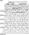
- Fig. 7 shows waveform diagrams each illustrating a voltage and DC voltages E D1 and E D2 output from each of three-level converters 31 to 35 in the state where a carrier signal on the first stage is defined as a reference phase.
- Fig. 7 representatively shows a U-phase voltage and an X-phase voltage that are output from the single-phase 3-level circuit ( Fig. 2 ).
- the high/low levels between the voltage command and each of the U-phase and X-phase triangular waves are compared. Based on the comparison results, it is determined how to combine turning-on and turning-off of the switching elements.
- the U-phase triangular wave on the first stage corresponds to a signal having a frequency that is 6 times as high as the voltage command and being in synchronization with the voltage command.
- the U-phase triangular wave on the first stage has a minimum value of 0V and a maximum value that is higher than the positive peak voltage of the voltage command.
- the X-phase triangular wave on the first stage corresponds to a signal that is in phase with the U-phase triangular wave on the first stage.
- the X-phase triangular wave on the first stage has a minimum value lower than the negative peak voltage of the voltage command and a maximum value of 0V.
- switching elements G U1 and G U2 are turned on and switching elements G U3 and G U4 are turned off.
- switching element G U2 is turned on and switching elements G U1 , G U3 and G U4 are turned off.
- switching element G U3 is turned on and switching elements G U1 , G U2 and G U4 are turned off.
- switching elements G U3 and G U4 are turned on and switching elements G U1 and G U2 are turned off.
- switching elements G X3 and G X4 are turned on and switching elements U X1 and G X2 are turned off.
- switching element G X3 is turned on and switching elements G X1 , G X2 and G X4 are turned off.
- switching element G X2 is turned on and switching elements G X1 , G X3 and G X4 are turned off.
- switching elements G X1 and G X2 are turned on and switching elements G X3 and G X4 are turned off.
- the single-phase 3-level circuit experiences a time period during which neutral point C as shown in Fig. 3 is connected to the AC system through the switching elements and the diodes.
- each of 3-level converters 31 to 35 the high/low levels between the voltage command and the carrier signals (the U-phase triangular wave and the X-phase triangular wave) are compared. Based on the comparison results, it is determined how to combine turning-on and turning-off of the switching elements. Consequently, in each of 3-level converters 31 to 35, there occurs: a switching pattern in which the potential at neutral point C rises; and a switching pattern in which the potential at neutral point C falls. As a result, in light of the entire power conversion device, a time period during which the potential at neutral point C rises and a time period during which the potential at neutral point C falls occur in one cycle of the voltage command, as shown on the lowermost stage in Fig. 7 .
- Fig. 8 shows waveform diagrams illustrating the results of a simulation performed for an output current, DC voltages E D1 and E D2 , and an output voltage from the power conversion device in the case where the carrier signal on the first stage is defined as a reference phase.
- the simulation in Fig. 8 is performed assuming the case where each of 3-level converters 31 to 35 in the power conversion device performs the operation shown in Fig. 7 .
- negative-side DC voltage E D2 when comparing positive-side DC voltage E D1 and negative-side DC voltage E D2 , negative-side DC voltage E D2 is higher than positive-side DC voltage E D1 , and an imbalance occurs between the positive-side DC voltage and the negative-side DC voltage. Accordingly, the potential at neutral point C is deviated toward the positive side, so that a voltage may be excessively applied to switching elements.
- capacitor voltage balance control circuit 180 ( Fig. 5 )
- the polarity of compensation amount BI1 is switched as the polarity of the output current changes.
- the waveform of the output voltage is distorted under the influence of pulsation of the output current.
- Fig. 9 shows waveform diagrams each illustrating a voltage and DC voltages E D1 and E D2 output from each of three-level converters 31 to 35 in the state where a carrier signal on the third stage is defined as a reference phase.
- Fig. 9 representatively shows a U-phase voltage and an X-phase voltage that are output from the single-phase 3-level circuit ( Fig. 2 ).
- the zero crossing point of the voltage command coincide with the zero crossing point of the carrier signal on the third stage (not shown) in place of the carrier signal on the first stage.
- remaining four carrier signals are generated based on this carrier signal on the third stage as a reference phase.
- the carrier signal on the fourth stage is obtained by delaying the phase of the carrier signal on the third stage by prescribed amount ⁇ s.
- the carrier signal on the fifth stage is obtained by delaying the phase of the carrier signal on the fourth stage by prescribed amount ⁇ s.
- the carrier signal on the first stage is obtained by delaying the phase of the carrier signal on the fifth stage by prescribed amount ⁇ s.
- the carrier signal on the second stage is obtained by delaying the phase of the carrier signal on the first stage by prescribed amount ⁇ s.
- the high/low levels between the voltage command and each of the U-phase and X-phase triangular waves are compared. Based on the comparison results, it is determined how to combine turning-on and turning-off of the switching elements. Then, when the switching elements are turned on and off, there occurs a time period during which neutral point C is connected to the AC system through the switching elements and the diodes, thereby producing a switching pattern in which the potential at neutral point C rises and a switching pattern in which the potential at neutral point C falls.
- each of 3-level converters 31 to 35 there occurs: a switching pattern in which the potential at neutral point C rises; and a switching pattern in which the potential at neutral point C falls, as described above. Accordingly, in light of the entire power conversion device, there occurs in one cycle of the voltage command: a time period during which the potential at neutral point C rises; and a time period during which the potential at neutral point C falls, as shown on the lowermost stage in Fig. 9 .
- Fig. 10 shows waveform diagrams illustrating the results of a simulation performed for an output current, DC voltages E D1 and E D2 , and an output voltage from the power conversion device in the case where the carrier signal on the third stage is defined as a reference phase. This simulation is performed assuming the case where each of 3-level converters 31 to 35 in the power conversion device performs an operation shown in Fig. 9 .
- positive-side DC voltage E D1 and negative-side DC voltage E D2 are almost equal, and an imbalance does not occur between these two DC voltages. Furthermore, since pulsation of the output current is relatively small, distortion of the output voltage waveform resulting from the change in output current polarity is also suppressed.
- the imbalance between positive-side DC voltage E D1 and negative-side DC voltage E D2 is less in the case where the carrier signal on the third stage is defined as a reference phase than in the case where the carrier signal on the first stage is defined as a reference phase.
- the phase of the carrier signal exerts a significant influence upon the potential at the neutral point in the DC voltage balance control.
- control device 10 corrects the reference phase of the carrier signal such that positive-side DC voltage E D1 and negative-side DC voltage E D2 are balanced with each other.
- control device 10 includes a carrier phase correction unit 26 as a configuration for correcting the reference phase of the carrier signal.
- Carrier phase correction unit 26 calculates a correction amount ⁇ of the reference phase according to DC voltage E D1 on capacitor C11 detected by voltage sensor 8 and DC voltage E D2 on capacitor C12 detected by voltage sensor 9. Then, carrier phase correction unit 26 outputs the calculated correction amount ⁇ to carrier signal generation unit 24.
- Fig. 11 is a functional block diagram of carrier phase correction unit 26 shown in Fig. 4 .
- carrier phase correction unit 26 includes a subtractor 260 and a PI calculation unit 262.
- PI calculation unit 262 calculates correction amount ⁇ by subjecting voltage difference E D to a proportional integral operation. PI calculation unit 262 calculates correction amount ⁇ for implementing the phase relation between the carrier signal and the voltage command such that voltage difference E D becomes zero, as shown in Fig. 9 .
- carrier signal generation unit 24 shifts the phase of the generated carrier signal by correction amount ⁇ .
- Fig. 12 is a diagram illustrating correction of the phase of the carrier signal in carrier signal generation unit 24.
- carrier signal generation unit 24 calculates a frequency of the AC system based on phase ⁇ detected by PLL circuit 22, to generate a carrier signal having a frequency that is an integral multiple (for example, 6 times) of the frequency of the AC system. As shown on the upper stage in Fig. 12 , the zero crossing point of the generated carrier signal coincides with the zero crossing point of the voltage command.
- Carrier signal generation unit 24 shifts the phase of this carrier signal by correction amount ⁇ , as shown on the lower stage in Fig. 12 .
- Carrier signal generation unit 24 outputs the corrected carrier signal to PWM pulse generation unit 20.
- PWM pulse generation unit 20 uses the corrected carrier signal to generate five carrier signals corresponding to five 3-level converters 31 to 35.
- PWM pulse generation unit 20 defines the corrected carrier signal as a carrier signal on the first stage.
- Fig. 12 shows a U-phase triangular wave on the first stage and an X-phase triangular wave on the first stage each acting as a carrier signal on the first stage.
- PWM pulse generation unit 20 generates remaining four carrier signals based on this carrier signal on the first stage as a reference phase.
- PWM pulse generation unit 20 compares the high/low levels between three-phase voltage commands V u2 *, V v2 * and V w2 * and each of the five carrier signals, thereby generating switching control signals S1 to S5 for controlling the switching elements in 3-level converters 31 to 35 to turn on and off.
- the power conversion device having a plurality of 3-level converters that are multiple-connected to each other can keep the balance between the positive-side DC voltage and the negative-side DC voltage by correcting the reference phase of the carrier signal according to the voltage difference between the positive-side DC voltage and the negative-side DC voltage.
- the effectiveness of DC voltage balance control is improved, variations in neutral point potential can be reliably suppressed.
Landscapes
- Engineering & Computer Science (AREA)
- Power Engineering (AREA)
- Inverter Devices (AREA)
Claims (1)
- Dispositif de conversion d'énergie, comprenant :une pluralité de convertisseurs à 3 niveaux (31, 32, 33, 34, 35) connectés mutuellement en série à une alimentation CA ; etun dispositif de contrôle (10), configuré pour contrôler des opérations de la pluralité de convertisseurs à 3 niveaux (31, 32, 33, 34, 35),chaque convertisseur de la pluralité de convertisseurs à 3 niveaux (31, 32, 33, 34, 35) étant agencé entre l'alimentation CA et chacun d'un bus positif CC (5), d'un bus négatif CC (6) et d'un bus neutre CC (7), et configuré pour convertir une tension CC en une tension CA ayant trois valeurs de tension,un premier condensateur (C11) et un second condensateur (C12) étant connectés en série entre le bus positif CC (5) et le bus négatif CC (6), et un point de connexion entre le premier condensateur (C11) et le second condensateur (C12) étant connecté au bus neutre CC (7), etle dispositif de contrôle (10) comprenant :une unité de calcul (18), configurée pour générer une quantité de compensation (B12) pour compenser le déséquilibre entre une tension (ED1) aux deux extrémités du premier condensateur (C11) et une tension (ED2) aux deux extrémités du second condensateur (C12), et ajouter la quantité de compensation (B12) à une commande de tension (Vu1*, Vv1*, Vw1*) pour générer une commande de tension de sortie (Vu2*, Vv2*, Vw2*) pour la pluralité de convertisseurs à 3 niveaux (31, 32, 33, 34, 35),une unité de génération de signal porteur (24), configurée pour générer un signal porteur ayant un point de passage par zéro coïncidant avec celui de la commande de tension de sortie (Vu2*, Vv2*, Vw2*),une unité de correction (26), configurée pour calculer une quantité de correction Δθ de la phase du signal porteur sur la base de la différence de tension entre la tension (ED1) aux deux extrémités du premier condensateur (C11) et la tension (ED2) aux deux extrémités du second condensateur (C12), l'unité de génération de signal porteur (24) étant en outre configurée pour déphaser le signal porteur de la quantité de correction Δθ, etune unité de contrôle de modulation d'impulsions en largeur (20), configurée pour : (i) retarder la phase d'une quantité prescrite sur la base du signal porteur corrigé en phase par l'unité de correction (26) en tant que phase de référence pour générer une pluralité de signaux porteurs ; et (ii) comparer la commande de tension de sortie (Vu2*, Vv2*, Vw2*) et chaque signal porteur de la pluralité de signaux porteurs pour générer une commande de contrôle (S1, S2, S3, S4, S5) pour chaque convertisseur de la pluralité de convertisseurs à 3 niveaux (31, 32, 33, 34, 35).
Applications Claiming Priority (1)
| Application Number | Priority Date | Filing Date | Title |
|---|---|---|---|
| PCT/JP2014/050020 WO2015102049A1 (fr) | 2014-01-06 | 2014-01-06 | Système de conversion d'énergie électrique |
Publications (3)
| Publication Number | Publication Date |
|---|---|
| EP3093976A1 EP3093976A1 (fr) | 2016-11-16 |
| EP3093976A4 EP3093976A4 (fr) | 2017-06-21 |
| EP3093976B1 true EP3093976B1 (fr) | 2019-04-17 |
Family
ID=53493397
Family Applications (1)
| Application Number | Title | Priority Date | Filing Date |
|---|---|---|---|
| EP14876755.1A Active EP3093976B1 (fr) | 2014-01-06 | 2014-01-06 | Système de conversion d'énergie électrique |
Country Status (5)
| Country | Link |
|---|---|
| US (1) | US9755551B2 (fr) |
| EP (1) | EP3093976B1 (fr) |
| JP (1) | JP6178433B2 (fr) |
| CN (1) | CN105900328B (fr) |
| WO (1) | WO2015102049A1 (fr) |
Families Citing this family (9)
| Publication number | Priority date | Publication date | Assignee | Title |
|---|---|---|---|---|
| JP6426462B2 (ja) * | 2014-12-24 | 2018-11-21 | 株式会社東芝 | 電力変換装置およびその制御方法 |
| US10123443B2 (en) * | 2014-12-25 | 2018-11-06 | Fuji Electric Co., Ltd. | Semiconductor device |
| KR101869279B1 (ko) * | 2015-10-05 | 2018-06-21 | 금호전기주식회사 | Led 램프 |
| TWI630784B (zh) * | 2016-11-30 | 2018-07-21 | 國立清華大學 | 中性點箝位換流器 |
| EP3771086A4 (fr) * | 2018-03-19 | 2021-03-31 | Mitsubishi Electric Corporation | Dispositif de conversion de puissance et système d'attaque de machine rotative |
| JP7249238B2 (ja) * | 2019-08-09 | 2023-03-30 | 東芝三菱電機産業システム株式会社 | 直列多重電力変換装置 |
| KR102597788B1 (ko) * | 2019-09-05 | 2023-11-02 | 도시바 미쓰비시덴키 산교시스템 가부시키가이샤 | 전력 변환 장치 |
| JP7371545B2 (ja) * | 2020-03-18 | 2023-10-31 | 富士電機株式会社 | 電力変換装置およびその制御方法 |
| CN114977861A (zh) * | 2022-07-29 | 2022-08-30 | 深圳市首航新能源股份有限公司 | 一种母线电压补偿方法、电子设备及其系统 |
Family Cites Families (22)
| Publication number | Priority date | Publication date | Assignee | Title |
|---|---|---|---|---|
| JP2500140B2 (ja) * | 1993-02-01 | 1996-05-29 | 株式会社東芝 | 中性点クランプ式コンバ―タの制御装置 |
| JP2888104B2 (ja) | 1993-09-01 | 1999-05-10 | 株式会社日立製作所 | 電力変換装置 |
| JP3186369B2 (ja) | 1993-09-09 | 2001-07-11 | 富士電機株式会社 | 3レベルインバータの制御回路 |
| JP3248321B2 (ja) * | 1993-11-10 | 2002-01-21 | 富士電機株式会社 | 3レベルインバータの制御回路 |
| JPH07245969A (ja) * | 1994-03-02 | 1995-09-19 | Toshiba Corp | 電力変換装置 |
| JPH09149658A (ja) * | 1995-11-24 | 1997-06-06 | Hitachi Ltd | 直列多重型インバータ装置 |
| DE19729479A1 (de) | 1997-07-10 | 1999-01-14 | Abb Daimler Benz Transp | Pulsweitenmodulationsverfahren für in Serie geschaltete Umrichter |
| JP4698305B2 (ja) * | 2005-07-05 | 2011-06-08 | 株式会社日立メディコ | 電源装置及びこれを用いた磁気共鳴イメージング装置 |
| JP5165918B2 (ja) * | 2007-04-26 | 2013-03-21 | 株式会社東芝 | 鉄道車両駆動制御システム |
| US7573732B2 (en) * | 2007-05-25 | 2009-08-11 | General Electric Company | Protective circuit and method for multi-level converter |
| CN102714469B (zh) * | 2010-01-13 | 2015-01-21 | 株式会社东芝 | 系统联合逆变器 |
| EP2348627A1 (fr) * | 2010-01-25 | 2011-07-27 | ABB Research Ltd. | Convertisseur et procédé pour l'operation d'un circuit convertisseur à plusieurs niveaux |
| EP2537244A1 (fr) | 2010-03-10 | 2012-12-26 | ABB Schweiz AG | Procédé pour faire fonctionner un circuit convertisseur ainsi que dispositif pour mettre en oeuvre le procédé |
| US8441820B2 (en) * | 2010-09-29 | 2013-05-14 | General Electric Company | DC-link voltage balancing system and method for multilevel converters |
| ES2402462B1 (es) * | 2010-11-08 | 2014-03-28 | Ingeteam Technology, S.A | Método de control para la conversión de energía, y convertidor electrónico de potencia adaptado para llevar a cabo dicho método |
| JP5734672B2 (ja) * | 2011-01-12 | 2015-06-17 | 株式会社東芝 | 半導体電力変換装置 |
| JP2013223279A (ja) * | 2012-04-13 | 2013-10-28 | Toshiba Corp | 電力変換装置 |
| CN104798297B (zh) * | 2012-11-21 | 2018-04-17 | 奥的斯电梯公司 | 中性点箝位多电平转换器 |
| EP3065278B1 (fr) * | 2013-10-30 | 2019-08-28 | Mitsubishi Electric Corporation | Dispositif de conversion cc/cc et système de commande de pilote de charge |
| US9325252B2 (en) * | 2014-01-13 | 2016-04-26 | Rockwell Automation Technologies, Inc. | Multilevel converter systems and sinusoidal pulse width modulation methods |
| JP6237400B2 (ja) * | 2014-03-27 | 2017-11-29 | 株式会社安川電機 | 発電装置、制御装置、制御方法、発電システム、電力変換装置及びシステム |
| CN105099241B (zh) * | 2014-04-18 | 2019-03-19 | 通用电气公司 | 控制器、电能变换系统和方法 |
-
2014
- 2014-01-06 WO PCT/JP2014/050020 patent/WO2015102049A1/fr not_active Ceased
- 2014-01-06 CN CN201480072465.6A patent/CN105900328B/zh active Active
- 2014-01-06 JP JP2015555855A patent/JP6178433B2/ja active Active
- 2014-01-06 US US15/109,219 patent/US9755551B2/en active Active
- 2014-01-06 EP EP14876755.1A patent/EP3093976B1/fr active Active
Non-Patent Citations (1)
| Title |
|---|
| None * |
Also Published As
| Publication number | Publication date |
|---|---|
| EP3093976A1 (fr) | 2016-11-16 |
| US9755551B2 (en) | 2017-09-05 |
| JPWO2015102049A1 (ja) | 2017-03-23 |
| CN105900328B (zh) | 2018-11-06 |
| EP3093976A4 (fr) | 2017-06-21 |
| CN105900328A (zh) | 2016-08-24 |
| JP6178433B2 (ja) | 2017-08-09 |
| WO2015102049A1 (fr) | 2015-07-09 |
| US20160329834A1 (en) | 2016-11-10 |
Similar Documents
| Publication | Publication Date | Title |
|---|---|---|
| US10224830B2 (en) | System and method for controlling a back-to-back three-level converter with voltage ripple compensation | |
| US9755551B2 (en) | Power conversion device | |
| Akagi et al. | Control and performance of a transformerless cascade PWM STATCOM with star configuration | |
| US10826378B2 (en) | Power conversion apparatus for interconnection with a three-phrase ac power supply | |
| US9768710B2 (en) | Converter | |
| JP5993675B2 (ja) | 電力変換装置,電力変換システム及び電力変換装置の制御方法 | |
| EP2491644B1 (fr) | Système et procédé permettant de compenser un déséquilibre de tension d'entrée dans des onduleurs à multiniveaux ou analogues | |
| US9013906B2 (en) | Power system-interconnected inverter device | |
| US12015354B2 (en) | Power conversion device capable of suppressing a harmonic component in an output voltage from an arm that increases after bypass of a failed converter cell | |
| US20130163292A1 (en) | Mid-point voltage control | |
| US11211879B2 (en) | Capacitor size reduction and lifetime extension for cascaded H-bridge drives | |
| JP6076222B2 (ja) | 電力変換装置 | |
| US11218079B2 (en) | Power conversion device | |
| US11336169B2 (en) | Power conversion device | |
| JP6538544B2 (ja) | 自励式無効電力補償装置 | |
| WO2014111595A1 (fr) | Convertisseur multiniveaux avec cellules hybrides en pont complet | |
| JP2018129963A (ja) | 電力変換器の制御装置 | |
| JP5904883B2 (ja) | 変圧器多重電力変換装置 | |
| Wen et al. | A new multilevel inverter-hexagram inverter for medium voltage adjustable speed drive systems Part II. Three-phase motor drive | |
| CN115398789B (zh) | 用分离dc链路控制多电平逆变器的方法 | |
| Ananth et al. | Multi-level Inverters and its application of STATCOM using SVPWM and SPWM Techniques | |
| Itoh et al. | Experimental verification of a multi-level inverter with H-bridge clamp circuit for single-phase three-wire grid connection | |
| WO2023214462A1 (fr) | Dispositif de conversion de puissance | |
| JP2025088984A (ja) | 電力変換システム及び制御方法 | |
| Xiao | Improvements in sensorless direct torque control for matrix converter driven interior permanent magnet synchronous machine |
Legal Events
| Date | Code | Title | Description |
|---|---|---|---|
| PUAI | Public reference made under article 153(3) epc to a published international application that has entered the european phase |
Free format text: ORIGINAL CODE: 0009012 |
|
| 17P | Request for examination filed |
Effective date: 20160607 |
|
| AK | Designated contracting states |
Kind code of ref document: A1 Designated state(s): AL AT BE BG CH CY CZ DE DK EE ES FI FR GB GR HR HU IE IS IT LI LT LU LV MC MK MT NL NO PL PT RO RS SE SI SK SM TR |
|
| AX | Request for extension of the european patent |
Extension state: BA ME |
|
| DAX | Request for extension of the european patent (deleted) | ||
| A4 | Supplementary search report drawn up and despatched |
Effective date: 20170522 |
|
| RIC1 | Information provided on ipc code assigned before grant |
Ipc: H02M 7/487 20070101AFI20170516BHEP |
|
| STAA | Information on the status of an ep patent application or granted ep patent |
Free format text: STATUS: EXAMINATION IS IN PROGRESS |
|
| 17Q | First examination report despatched |
Effective date: 20180423 |
|
| GRAP | Despatch of communication of intention to grant a patent |
Free format text: ORIGINAL CODE: EPIDOSNIGR1 |
|
| STAA | Information on the status of an ep patent application or granted ep patent |
Free format text: STATUS: GRANT OF PATENT IS INTENDED |
|
| RIC1 | Information provided on ipc code assigned before grant |
Ipc: H02M 7/487 20070101AFI20181024BHEP Ipc: H02M 7/5395 20060101ALI20181024BHEP Ipc: H02M 7/49 20070101ALI20181024BHEP |
|
| INTG | Intention to grant announced |
Effective date: 20181203 |
|
| GRAS | Grant fee paid |
Free format text: ORIGINAL CODE: EPIDOSNIGR3 |
|
| GRAA | (expected) grant |
Free format text: ORIGINAL CODE: 0009210 |
|
| STAA | Information on the status of an ep patent application or granted ep patent |
Free format text: STATUS: THE PATENT HAS BEEN GRANTED |
|
| AK | Designated contracting states |
Kind code of ref document: B1 Designated state(s): AL AT BE BG CH CY CZ DE DK EE ES FI FR GB GR HR HU IE IS IT LI LT LU LV MC MK MT NL NO PL PT RO RS SE SI SK SM TR |
|
| REG | Reference to a national code |
Ref country code: GB Ref legal event code: FG4D |
|
| REG | Reference to a national code |
Ref country code: CH Ref legal event code: EP |
|
| REG | Reference to a national code |
Ref country code: DE Ref legal event code: R096 Ref document number: 602014045109 Country of ref document: DE |
|
| REG | Reference to a national code |
Ref country code: AT Ref legal event code: REF Ref document number: 1122651 Country of ref document: AT Kind code of ref document: T Effective date: 20190515 Ref country code: IE Ref legal event code: FG4D |
|
| REG | Reference to a national code |
Ref country code: NL Ref legal event code: MP Effective date: 20190417 |
|
| REG | Reference to a national code |
Ref country code: LT Ref legal event code: MG4D |
|
| PG25 | Lapsed in a contracting state [announced via postgrant information from national office to epo] |
Ref country code: NL Free format text: LAPSE BECAUSE OF FAILURE TO SUBMIT A TRANSLATION OF THE DESCRIPTION OR TO PAY THE FEE WITHIN THE PRESCRIBED TIME-LIMIT Effective date: 20190417 |
|
| PG25 | Lapsed in a contracting state [announced via postgrant information from national office to epo] |
Ref country code: HR Free format text: LAPSE BECAUSE OF FAILURE TO SUBMIT A TRANSLATION OF THE DESCRIPTION OR TO PAY THE FEE WITHIN THE PRESCRIBED TIME-LIMIT Effective date: 20190417 Ref country code: FI Free format text: LAPSE BECAUSE OF FAILURE TO SUBMIT A TRANSLATION OF THE DESCRIPTION OR TO PAY THE FEE WITHIN THE PRESCRIBED TIME-LIMIT Effective date: 20190417 Ref country code: LT Free format text: LAPSE BECAUSE OF FAILURE TO SUBMIT A TRANSLATION OF THE DESCRIPTION OR TO PAY THE FEE WITHIN THE PRESCRIBED TIME-LIMIT Effective date: 20190417 Ref country code: AL Free format text: LAPSE BECAUSE OF FAILURE TO SUBMIT A TRANSLATION OF THE DESCRIPTION OR TO PAY THE FEE WITHIN THE PRESCRIBED TIME-LIMIT Effective date: 20190417 Ref country code: ES Free format text: LAPSE BECAUSE OF FAILURE TO SUBMIT A TRANSLATION OF THE DESCRIPTION OR TO PAY THE FEE WITHIN THE PRESCRIBED TIME-LIMIT Effective date: 20190417 Ref country code: SE Free format text: LAPSE BECAUSE OF FAILURE TO SUBMIT A TRANSLATION OF THE DESCRIPTION OR TO PAY THE FEE WITHIN THE PRESCRIBED TIME-LIMIT Effective date: 20190417 Ref country code: NO Free format text: LAPSE BECAUSE OF FAILURE TO SUBMIT A TRANSLATION OF THE DESCRIPTION OR TO PAY THE FEE WITHIN THE PRESCRIBED TIME-LIMIT Effective date: 20190717 Ref country code: PT Free format text: LAPSE BECAUSE OF FAILURE TO SUBMIT A TRANSLATION OF THE DESCRIPTION OR TO PAY THE FEE WITHIN THE PRESCRIBED TIME-LIMIT Effective date: 20190817 |
|
| PG25 | Lapsed in a contracting state [announced via postgrant information from national office to epo] |
Ref country code: GR Free format text: LAPSE BECAUSE OF FAILURE TO SUBMIT A TRANSLATION OF THE DESCRIPTION OR TO PAY THE FEE WITHIN THE PRESCRIBED TIME-LIMIT Effective date: 20190718 Ref country code: PL Free format text: LAPSE BECAUSE OF FAILURE TO SUBMIT A TRANSLATION OF THE DESCRIPTION OR TO PAY THE FEE WITHIN THE PRESCRIBED TIME-LIMIT Effective date: 20190417 Ref country code: LV Free format text: LAPSE BECAUSE OF FAILURE TO SUBMIT A TRANSLATION OF THE DESCRIPTION OR TO PAY THE FEE WITHIN THE PRESCRIBED TIME-LIMIT Effective date: 20190417 Ref country code: BG Free format text: LAPSE BECAUSE OF FAILURE TO SUBMIT A TRANSLATION OF THE DESCRIPTION OR TO PAY THE FEE WITHIN THE PRESCRIBED TIME-LIMIT Effective date: 20190717 Ref country code: RS Free format text: LAPSE BECAUSE OF FAILURE TO SUBMIT A TRANSLATION OF THE DESCRIPTION OR TO PAY THE FEE WITHIN THE PRESCRIBED TIME-LIMIT Effective date: 20190417 |
|
| REG | Reference to a national code |
Ref country code: AT Ref legal event code: MK05 Ref document number: 1122651 Country of ref document: AT Kind code of ref document: T Effective date: 20190417 |
|
| PG25 | Lapsed in a contracting state [announced via postgrant information from national office to epo] |
Ref country code: IS Free format text: LAPSE BECAUSE OF FAILURE TO SUBMIT A TRANSLATION OF THE DESCRIPTION OR TO PAY THE FEE WITHIN THE PRESCRIBED TIME-LIMIT Effective date: 20190817 |
|
| REG | Reference to a national code |
Ref country code: DE Ref legal event code: R097 Ref document number: 602014045109 Country of ref document: DE |
|
| PG25 | Lapsed in a contracting state [announced via postgrant information from national office to epo] |
Ref country code: SK Free format text: LAPSE BECAUSE OF FAILURE TO SUBMIT A TRANSLATION OF THE DESCRIPTION OR TO PAY THE FEE WITHIN THE PRESCRIBED TIME-LIMIT Effective date: 20190417 Ref country code: EE Free format text: LAPSE BECAUSE OF FAILURE TO SUBMIT A TRANSLATION OF THE DESCRIPTION OR TO PAY THE FEE WITHIN THE PRESCRIBED TIME-LIMIT Effective date: 20190417 Ref country code: CZ Free format text: LAPSE BECAUSE OF FAILURE TO SUBMIT A TRANSLATION OF THE DESCRIPTION OR TO PAY THE FEE WITHIN THE PRESCRIBED TIME-LIMIT Effective date: 20190417 Ref country code: RO Free format text: LAPSE BECAUSE OF FAILURE TO SUBMIT A TRANSLATION OF THE DESCRIPTION OR TO PAY THE FEE WITHIN THE PRESCRIBED TIME-LIMIT Effective date: 20190417 Ref country code: AT Free format text: LAPSE BECAUSE OF FAILURE TO SUBMIT A TRANSLATION OF THE DESCRIPTION OR TO PAY THE FEE WITHIN THE PRESCRIBED TIME-LIMIT Effective date: 20190417 Ref country code: DK Free format text: LAPSE BECAUSE OF FAILURE TO SUBMIT A TRANSLATION OF THE DESCRIPTION OR TO PAY THE FEE WITHIN THE PRESCRIBED TIME-LIMIT Effective date: 20190417 |
|
| PLBE | No opposition filed within time limit |
Free format text: ORIGINAL CODE: 0009261 |
|
| STAA | Information on the status of an ep patent application or granted ep patent |
Free format text: STATUS: NO OPPOSITION FILED WITHIN TIME LIMIT |
|
| PG25 | Lapsed in a contracting state [announced via postgrant information from national office to epo] |
Ref country code: SM Free format text: LAPSE BECAUSE OF FAILURE TO SUBMIT A TRANSLATION OF THE DESCRIPTION OR TO PAY THE FEE WITHIN THE PRESCRIBED TIME-LIMIT Effective date: 20190417 Ref country code: IT Free format text: LAPSE BECAUSE OF FAILURE TO SUBMIT A TRANSLATION OF THE DESCRIPTION OR TO PAY THE FEE WITHIN THE PRESCRIBED TIME-LIMIT Effective date: 20190417 |
|
| 26N | No opposition filed |
Effective date: 20200120 |
|
| PG25 | Lapsed in a contracting state [announced via postgrant information from national office to epo] |
Ref country code: TR Free format text: LAPSE BECAUSE OF FAILURE TO SUBMIT A TRANSLATION OF THE DESCRIPTION OR TO PAY THE FEE WITHIN THE PRESCRIBED TIME-LIMIT Effective date: 20190417 |
|
| PG25 | Lapsed in a contracting state [announced via postgrant information from national office to epo] |
Ref country code: SI Free format text: LAPSE BECAUSE OF FAILURE TO SUBMIT A TRANSLATION OF THE DESCRIPTION OR TO PAY THE FEE WITHIN THE PRESCRIBED TIME-LIMIT Effective date: 20190417 |
|
| PG25 | Lapsed in a contracting state [announced via postgrant information from national office to epo] |
Ref country code: MC Free format text: LAPSE BECAUSE OF FAILURE TO SUBMIT A TRANSLATION OF THE DESCRIPTION OR TO PAY THE FEE WITHIN THE PRESCRIBED TIME-LIMIT Effective date: 20190417 |
|
| REG | Reference to a national code |
Ref country code: CH Ref legal event code: PL |
|
| REG | Reference to a national code |
Ref country code: BE Ref legal event code: MM Effective date: 20200131 |
|
| REG | Reference to a national code |
Ref country code: DE Ref legal event code: R082 Ref document number: 602014045109 Country of ref document: DE Representative=s name: VENNER SHIPLEY GERMANY LLP, DE Ref country code: DE Ref legal event code: R082 Ref document number: 602014045109 Country of ref document: DE Representative=s name: VENNER SHIPLEY LLP, DE |
|
| PG25 | Lapsed in a contracting state [announced via postgrant information from national office to epo] |
Ref country code: LU Free format text: LAPSE BECAUSE OF NON-PAYMENT OF DUE FEES Effective date: 20200106 |
|
| PG25 | Lapsed in a contracting state [announced via postgrant information from national office to epo] |
Ref country code: BE Free format text: LAPSE BECAUSE OF NON-PAYMENT OF DUE FEES Effective date: 20200131 Ref country code: LI Free format text: LAPSE BECAUSE OF NON-PAYMENT OF DUE FEES Effective date: 20200131 Ref country code: CH Free format text: LAPSE BECAUSE OF NON-PAYMENT OF DUE FEES Effective date: 20200131 |
|
| PG25 | Lapsed in a contracting state [announced via postgrant information from national office to epo] |
Ref country code: IE Free format text: LAPSE BECAUSE OF NON-PAYMENT OF DUE FEES Effective date: 20200106 |
|
| PG25 | Lapsed in a contracting state [announced via postgrant information from national office to epo] |
Ref country code: MT Free format text: LAPSE BECAUSE OF FAILURE TO SUBMIT A TRANSLATION OF THE DESCRIPTION OR TO PAY THE FEE WITHIN THE PRESCRIBED TIME-LIMIT Effective date: 20190417 Ref country code: CY Free format text: LAPSE BECAUSE OF FAILURE TO SUBMIT A TRANSLATION OF THE DESCRIPTION OR TO PAY THE FEE WITHIN THE PRESCRIBED TIME-LIMIT Effective date: 20190417 |
|
| PG25 | Lapsed in a contracting state [announced via postgrant information from national office to epo] |
Ref country code: MK Free format text: LAPSE BECAUSE OF FAILURE TO SUBMIT A TRANSLATION OF THE DESCRIPTION OR TO PAY THE FEE WITHIN THE PRESCRIBED TIME-LIMIT Effective date: 20190417 |
|
| PGFP | Annual fee paid to national office [announced via postgrant information from national office to epo] |
Ref country code: GB Payment date: 20251127 Year of fee payment: 13 |
|
| PGFP | Annual fee paid to national office [announced via postgrant information from national office to epo] |
Ref country code: FR Payment date: 20251128 Year of fee payment: 13 |
|
| PGFP | Annual fee paid to national office [announced via postgrant information from national office to epo] |
Ref country code: DE Payment date: 20251203 Year of fee payment: 13 |