EP3093988A1 - Schaltung mit konstantem variablem schaltkreis - Google Patents
Schaltung mit konstantem variablem schaltkreis Download PDFInfo
- Publication number
- EP3093988A1 EP3093988A1 EP14877881.4A EP14877881A EP3093988A1 EP 3093988 A1 EP3093988 A1 EP 3093988A1 EP 14877881 A EP14877881 A EP 14877881A EP 3093988 A1 EP3093988 A1 EP 3093988A1
- Authority
- EP
- European Patent Office
- Prior art keywords
- circuit
- bidirectional switch
- constant variable
- series
- conductive
- Prior art date
- Legal status (The legal status is an assumption and is not a legal conclusion. Google has not performed a legal analysis and makes no representation as to the accuracy of the status listed.)
- Withdrawn
Links
- 230000002457 bidirectional effect Effects 0.000 claims abstract description 145
- 239000003990 capacitor Substances 0.000 claims description 47
- 230000004913 activation Effects 0.000 description 13
- 230000009849 deactivation Effects 0.000 description 13
- 238000010586 diagram Methods 0.000 description 6
- JMASRVWKEDWRBT-UHFFFAOYSA-N Gallium nitride Chemical compound [Ga]#N JMASRVWKEDWRBT-UHFFFAOYSA-N 0.000 description 4
- IJGRMHOSHXDMSA-UHFFFAOYSA-N Atomic nitrogen Chemical compound N#N IJGRMHOSHXDMSA-UHFFFAOYSA-N 0.000 description 2
- 229910002601 GaN Inorganic materials 0.000 description 2
- 230000005674 electromagnetic induction Effects 0.000 description 2
- GYHNNYVSQQEPJS-UHFFFAOYSA-N Gallium Chemical compound [Ga] GYHNNYVSQQEPJS-UHFFFAOYSA-N 0.000 description 1
- 230000008878 coupling Effects 0.000 description 1
- 238000010168 coupling process Methods 0.000 description 1
- 238000005859 coupling reaction Methods 0.000 description 1
- 238000001514 detection method Methods 0.000 description 1
- 238000007599 discharging Methods 0.000 description 1
- 230000000694 effects Effects 0.000 description 1
- 229910052733 gallium Inorganic materials 0.000 description 1
- 230000001939 inductive effect Effects 0.000 description 1
- 238000005259 measurement Methods 0.000 description 1
- 229910052757 nitrogen Inorganic materials 0.000 description 1
Images


Classifications
-
- H—ELECTRICITY
- H03—ELECTRONIC CIRCUITRY
- H03K—PULSE TECHNIQUE
- H03K17/00—Electronic switching or gating, i.e. not by contact-making and –breaking
- H03K17/51—Electronic switching or gating, i.e. not by contact-making and –breaking characterised by the components used
- H03K17/56—Electronic switching or gating, i.e. not by contact-making and –breaking characterised by the components used by the use, as active elements, of semiconductor devices
- H03K17/567—Circuits characterised by the use of more than one type of semiconductor device, e.g. BIMOS, composite devices such as IGBT
-
- H—ELECTRICITY
- H02—GENERATION; CONVERSION OR DISTRIBUTION OF ELECTRIC POWER
- H02M—APPARATUS FOR CONVERSION BETWEEN AC AND AC, BETWEEN AC AND DC, OR BETWEEN DC AND DC, AND FOR USE WITH MAINS OR SIMILAR POWER SUPPLY SYSTEMS; CONVERSION OF DC OR AC INPUT POWER INTO SURGE OUTPUT POWER; CONTROL OR REGULATION THEREOF
- H02M3/00—Conversion of DC power input into DC power output
- H02M3/22—Conversion of DC power input into DC power output with intermediate conversion into AC
- H02M3/24—Conversion of DC power input into DC power output with intermediate conversion into AC by static converters
- H02M3/28—Conversion of DC power input into DC power output with intermediate conversion into AC by static converters using discharge tubes with control electrode or semiconductor devices with control electrode to produce the intermediate AC
- H02M3/325—Conversion of DC power input into DC power output with intermediate conversion into AC by static converters using discharge tubes with control electrode or semiconductor devices with control electrode to produce the intermediate AC using devices of a triode or a transistor type requiring continuous application of a control signal
- H02M3/335—Conversion of DC power input into DC power output with intermediate conversion into AC by static converters using discharge tubes with control electrode or semiconductor devices with control electrode to produce the intermediate AC using devices of a triode or a transistor type requiring continuous application of a control signal using semiconductor devices only
- H02M3/33569—Conversion of DC power input into DC power output with intermediate conversion into AC by static converters using discharge tubes with control electrode or semiconductor devices with control electrode to produce the intermediate AC using devices of a triode or a transistor type requiring continuous application of a control signal using semiconductor devices only having several active switching elements
-
- H—ELECTRICITY
- H02—GENERATION; CONVERSION OR DISTRIBUTION OF ELECTRIC POWER
- H02M—APPARATUS FOR CONVERSION BETWEEN AC AND AC, BETWEEN AC AND DC, OR BETWEEN DC AND DC, AND FOR USE WITH MAINS OR SIMILAR POWER SUPPLY SYSTEMS; CONVERSION OF DC OR AC INPUT POWER INTO SURGE OUTPUT POWER; CONTROL OR REGULATION THEREOF
- H02M3/00—Conversion of DC power input into DC power output
- H02M3/01—Resonant DC/DC converters
-
- H—ELECTRICITY
- H03—ELECTRONIC CIRCUITRY
- H03K—PULSE TECHNIQUE
- H03K17/00—Electronic switching or gating, i.e. not by contact-making and –breaking
- H03K17/51—Electronic switching or gating, i.e. not by contact-making and –breaking characterised by the components used
- H03K17/56—Electronic switching or gating, i.e. not by contact-making and –breaking characterised by the components used by the use, as active elements, of semiconductor devices
- H03K17/687—Electronic switching or gating, i.e. not by contact-making and –breaking characterised by the components used by the use, as active elements, of semiconductor devices the devices being field-effect transistors
-
- H—ELECTRICITY
- H02—GENERATION; CONVERSION OR DISTRIBUTION OF ELECTRIC POWER
- H02M—APPARATUS FOR CONVERSION BETWEEN AC AND AC, BETWEEN AC AND DC, OR BETWEEN DC AND DC, AND FOR USE WITH MAINS OR SIMILAR POWER SUPPLY SYSTEMS; CONVERSION OF DC OR AC INPUT POWER INTO SURGE OUTPUT POWER; CONTROL OR REGULATION THEREOF
- H02M3/00—Conversion of DC power input into DC power output
- H02M3/22—Conversion of DC power input into DC power output with intermediate conversion into AC
- H02M3/24—Conversion of DC power input into DC power output with intermediate conversion into AC by static converters
- H02M3/28—Conversion of DC power input into DC power output with intermediate conversion into AC by static converters using discharge tubes with control electrode or semiconductor devices with control electrode to produce the intermediate AC
- H02M3/325—Conversion of DC power input into DC power output with intermediate conversion into AC by static converters using discharge tubes with control electrode or semiconductor devices with control electrode to produce the intermediate AC using devices of a triode or a transistor type requiring continuous application of a control signal
- H02M3/335—Conversion of DC power input into DC power output with intermediate conversion into AC by static converters using discharge tubes with control electrode or semiconductor devices with control electrode to produce the intermediate AC using devices of a triode or a transistor type requiring continuous application of a control signal using semiconductor devices only
- H02M3/33569—Conversion of DC power input into DC power output with intermediate conversion into AC by static converters using discharge tubes with control electrode or semiconductor devices with control electrode to produce the intermediate AC using devices of a triode or a transistor type requiring continuous application of a control signal using semiconductor devices only having several active switching elements
- H02M3/33576—Conversion of DC power input into DC power output with intermediate conversion into AC by static converters using discharge tubes with control electrode or semiconductor devices with control electrode to produce the intermediate AC using devices of a triode or a transistor type requiring continuous application of a control signal using semiconductor devices only having several active switching elements having at least one active switching element at the secondary side of an isolation transformer
- H02M3/33584—Bidirectional converters
-
- H—ELECTRICITY
- H02—GENERATION; CONVERSION OR DISTRIBUTION OF ELECTRIC POWER
- H02M—APPARATUS FOR CONVERSION BETWEEN AC AND AC, BETWEEN AC AND DC, OR BETWEEN DC AND DC, AND FOR USE WITH MAINS OR SIMILAR POWER SUPPLY SYSTEMS; CONVERSION OF DC OR AC INPUT POWER INTO SURGE OUTPUT POWER; CONTROL OR REGULATION THEREOF
- H02M7/00—Conversion of AC power input into DC power output; Conversion of DC power input into AC power output
- H02M7/42—Conversion of DC power input into AC power output without possibility of reversal
- H02M7/44—Conversion of DC power input into AC power output without possibility of reversal by static converters
- H02M7/48—Conversion of DC power input into AC power output without possibility of reversal by static converters using discharge tubes with control electrode or semiconductor devices with control electrode
- H02M7/4815—Resonant converters
- H02M7/4818—Resonant converters with means for adaptation of resonance frequency, e.g. by modification of capacitance or inductance of resonance circuits
-
- Y—GENERAL TAGGING OF NEW TECHNOLOGICAL DEVELOPMENTS; GENERAL TAGGING OF CROSS-SECTIONAL TECHNOLOGIES SPANNING OVER SEVERAL SECTIONS OF THE IPC; TECHNICAL SUBJECTS COVERED BY FORMER USPC CROSS-REFERENCE ART COLLECTIONS [XRACs] AND DIGESTS
- Y02—TECHNOLOGIES OR APPLICATIONS FOR MITIGATION OR ADAPTATION AGAINST CLIMATE CHANGE
- Y02B—CLIMATE CHANGE MITIGATION TECHNOLOGIES RELATED TO BUILDINGS, e.g. HOUSING, HOUSE APPLIANCES OR RELATED END-USER APPLICATIONS
- Y02B70/00—Technologies for an efficient end-user side electric power management and consumption
- Y02B70/10—Technologies improving the efficiency by using switched-mode power supplies [SMPS], i.e. efficient power electronics conversion e.g. power factor correction or reduction of losses in power supplies or efficient standby modes
Definitions
- the present invention relates to a circuit constant variable circuit.
- a resonant bidirectional converter includes a primary coil and a secondary coil that are coupled to each other through electromagnetic induction.
- the primary coil and the secondary coil are provided with a primary drive circuit and a secondary drive circuit, respectively.
- the primary drive circuit and the secondary drive circuit each include a full-bridge circuit including four switching elements (Patent Document 1).
- Patent Document 1 When power is output from the primary side to a load of the secondary side, the full-bridge circuit of the primary drive circuit is used as a switching circuit, and the full-bridge circuit of the secondary drive circuit is used as a rectifying circuit.
- the full-bridge circuit of the secondary drive circuit is used as a switching circuit, and the full-bridge circuit of the primary drive circuit is used as a rectifying circuit.
- the resonant bidirectional converter is configured to use the same resonant frequency when the full-bridge circuit of the primary drive circuit is used as a switching circuit and when the full-bridge circuit of the secondary drive circuit is used as a switching circuit.
- a resonant circuit having a variable resonant parameter is connected in series to the primary coil.
- a plurality of capacitors and coils that form the resonant circuit are selected to use the same resonant frequency when the primary drive circuit is used as a switching circuit and when the secondary drive circuit is used as a switching circuit.
- Patent Document 1 Japanese Laid-Open Patent Publication No. 2012-70491
- the above resonant circuit requires a plurality of capacitors and coils. In addition, only two resonant parameters of the resonant circuit can be selected.
- One aspect of the present invention is a circuit constant variable circuit that varies a circuit constant of a passive element of which impedance changes in accordance with a frequency of an alternating current.
- the circuit constant variable circuit includes a series circuit including a first bidirectional switch and a passive element that are connected in series.
- the circuit constant variable circuit further includes a second bidirectional switch connected in parallel to the series circuit.
- each of the first bidirectional switch and the second bidirectional switch include a GaN bidirectional switching device having a double-gate.
- each of the first bidirectional switch and the second bidirectional switch include two series circuits, each including a diode and an IGBT that are connected in series, and that the two series circuits be connected in parallel so that the two series circuits have polarities of different directions.
- each of the first bidirectional switch and the second bidirectional switch include two MOS transistors that are connected in series.
- the passive element include a capacitor or a coil.
- the passive element include a capacitor or a coil and that the capacitor and the coil be connected in series or in parallel.
- the circuit constant variable circuit include a control circuit that causes, at least once during a single cycle of the alternating current, the first bidirectional switch to be conductive in one direction while the second bidirectional switch is non-conductive in two directions, subsequently causes the first bidirectional switch to be conductive in the other direction, and then causes the first bidirectional switch and the second bidirectional switch to be conductive in two directions.
- control circuit control a time in which the first bidirectional switch is conductive in one direction and a time in which the first bidirectional switch is conductive in the other direction.
- One aspect of the present invention is a circuit constant variable circuit that varies a circuit constant of a passive element of which impedance changes in accordance with a frequency of an alternating current.
- the circuit constant variable circuit includes the passive element, a first bidirectional switch connected in series to the passive element, and a second bidirectional switch connected in parallel to the passive element.
- each of the first bidirectional switch and the second bidirectional switch include a GaN bidirectional switching device having a double-gate.
- each of the first bidirectional switch and the second bidirectional switch include two series circuits, each including a diode and an IGBT that are connected in series, and that the two series circuits be connected in parallel so that the two series circuits have polarities of different directions.
- each of the first bidirectional switch and the second bidirectional switch include two MOS transistors that are connected in series.
- the passive element include a capacitor or a coil.
- the passive element include a capacitor and a coil that are connected in series or in parallel.
- the circuit constant variable circuit include a control circuit that causes, at least once during a single cycle of the alternating current, the first bidirectional switch to be conductive in one direction while the second bidirectional switch is non-conductive in two directions, subsequently causes the first bidirectional switch to be conductive in the other direction, and then causes the first bidirectional switch and the second bidirectional switch to be conductive in two directions.
- control circuit control a time in which the first bidirectional switch is conductive in one direction and a time in which the first bidirectional switch is conductive in the other direction.
- the present calorie measurement device is capable of varying the circuit constant with a simple circuit configuration.
- the present invention provides a circuit that electrically controls and varies the circuit constant of a passive element, such as the capacitance of a capacitor or the inductance of a coil, with a simplified circuit configuration.
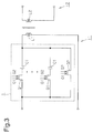
- a circuit constant variable circuit 1 includes a capacitor C1 serving as a passive element and a first bidirectional switch Q1 that are connected in series.
- the circuit constant variable circuit 1 further includes a second bidirectional switch Q2 that is connected in parallel to the series circuit. Alternating current is supplied to between two terminals P1 and P2 of the parallel circuit.
- the bidirectional switches Q1 and Q2 each include, for example, a gallium nitride (GaN) bidirectional switching device having a double-gate that includes a first gate terminal G1 and a second gate terminal G2.
- GaN gallium nitride
- the first bidirectional switch Q1 functions in four modes that are changed by activation and deactivation signals provided to the first gate terminal G1 and the second gate terminal G2 (the same applies to second bidirectional switch Q2).
- the first mode causes the first bidirectional switch Q1 (second bidirectional switch Q2) to be conductive from terminal P1 toward terminal P2 when the first gate terminal G1 is provided with the activation signal and the second gate terminal G2 is provided with the deactivation signal.
- the second mode causes the first bidirectional switch Q1 (second bidirectional switch 02) to be conductive from terminal P2 toward terminal P1 when the first gate terminal G1 is provided with the deactivation signal and the second gate terminal G2 is provided with the activation signal.
- the third mode causes the first bidirectional switch Q1 (second bidirectional switch Q2) to be conductive in any direction (fully conductive) between terminal P1 and terminal P2 when the first gate terminal G1 and the second gate terminal G2 are both provided with the activation signals.
- the fourth mode causes the first bidirectional switch Q1 (second bidirectional switch Q2) to be non-conductive in any direction (fully non-conductive) between terminal P1 and terminal P2 when the first gate terminal G1 and the second gate terminal G2 are both provided with the deactivation signals.
- a control circuit 10 is connected to the first gate terminals G1 and the second gate terminals G2 of the first and second bidirectional switches Q1 and Q2.
- the control circuit 10 outputs the activation and deactivation signals to the first and second gate terminals G1 and G2 of the first bidirectional switch Q1 to set the first bidirectional switch Q1 to any one of the first to fourth modes at a predetermined timing.
- the control circuit 10 outputs the activation and deactivation signals to the first and second gate terminals G1 and G2 of the second bidirectional switch Q2 to set the second bidirectional switch Q2 to any one of the first to fourth modes at a predetermined timing.
- circuit constant variable circuit 1 The operation of the circuit constant variable circuit 1 will now be described.
- the control circuit 10 controls the circuit constant variable circuit 1 by repeating steps 1 to 4, which will now be described.
- control circuit 10 sets the first bidirectional switch Q1 to the fourth mode and the second bidirectional switch Q2 to the third mode.
- control circuit 10 outputs the deactivation signal to both of the first and second gate terminals G1 and G2 of the first bidirectional switch Q1 to deactivate the first bidirectional switch Q1 (fully non-conductive). Further, the control circuit 10 outputs the activation signal to both of the first and second gate terminals G1 and G2 of the second bidirectional switch Q2 to activate the second bidirectional switch Q2 (fully conductive).
- Step 2 Chargeable Time Control
- the control circuit 10 sets the first bidirectional switch Q1 to the first mode and sets the second bidirectional switch Q2 to the fourth mode.
- control circuit 10 outputs the activation signal to the first gate terminal G1 of the first bidirectional switch Q1 (control circuit 10 continues to output deactivation signal to second gate terminal G2) so that the first bidirectional switch Q1 is conductive from terminal P1 toward terminal P2. Further, the control circuit 10 outputs the deactivation signal to the first and second gate terminals G1 and G2 of the second bidirectional switch Q2 to deactivate the second bidirectional switch Q2 (fully non-conductive).
- Step 3 Inverse-chargeable Time Control
- control circuit 10 sets the first bidirectional switch Q1 to the second mode and sets the second bidirectional switch Q2 to the fourth mode.
- control circuit 10 outputs the deactivation signal to the first gate terminal G1 of the first bidirectional switch Q1 and outputs the activation signal to the second gate terminal G2 so that the first bidirectional switch Q1 is conductive from terminal P2 toward terminal P1. Further, the control circuit 10 continues to output the deactivation signal to the first and second gate terminals G1 and G2 of the second bidirectional switch Q2 to deactivate the second bidirectional switch Q2 (fully non-conductive).
- Step 4 Residual Electric Charge Discharging
- the control circuit 10 sets the first bidirectional switch Q1 and the second bidirectional switch Q2 to the third mode.
- the timing for proceeding to step 4 may be determined based on the time in which the voltage between the terminals of the capacitor C1 becomes 0 V that is obtained through detection performed by a voltage detector or through tests, experiments, calculations, and the like that are performed in advance.
- control circuit 10 outputs the activation signal to the first and second gate terminals G1 and G2 of the first bidirectional switch Q1 to activate the first bidirectional switch Q1 (fully conductive). Further, the control circuit 10 outputs the activation signal to the first and second gate terminals G1 and G2 of the second bidirectional switch Q2 to activate the first bidirectional switch Q1 (fully conductive).
- the first and second bidirectional switches Q1 and Q2 are fully conductive so that the residual electric charge of the capacitor C1 is completely discharged.
- the control circuit 10 returns to the operation of step 1 and repeats the operations of steps 1 to 4 again.
- the control circuit 10 controls the operation time of steps 1 to 4, that is, the charge time and the inverse charge (discharge) time for the capacitor C1, based on the data obtained in advance through tests, experiments, calculations, and the like. This controls the accumulated amount of the electric charge in the capacitor C1 so that a virtual capacitance (circuit constant) of the capacitor C1 can be varied.
- the first embodiment has the advantages described below.
- the circuit constant variable circuit 1 includes the capacitor C1 and the first bidirectional switch Q1 that are connected in parallel.
- the circuit constant variable circuit 1 further includes the second bidirectional switch Q2 that is connected in series to the parallel circuit. Alternative current is supplied to between two terminals P1 and P2 of the parallel circuit.
- the bidirectional switches Q1 and Q2 each include, for example, a gallium nitride (Gan) bidirectional switching device having a double-gate that includes the first gate terminal G1 and the second gate terminal G2 in the same manner as the first embodiment.
- Ga gallium nitride
- the first bidirectional switch Q1 and the second bidirectional switch Q2 each function in four modes that are changed by activation and deactivation signals provided to the first gate terminal G1 and the second gate terminal G2.
- control circuit 10 is connected to the first gate terminal G1 and the second gate terminal G2 of the first and second bidirectional switches Q1 and Q2. That is, the control circuit 10 controls the first and second bidirectional switches Q1 and Q2 to control the capacitance (circuit constant) of the capacitor C1.
- circuit constant variable circuit 1 The operation of the circuit constant variable circuit 1 will now be described.
- the circuit constant variable circuit 1 of the second embodiment controls the capacitance (circuit constant) of the capacitor C1 by repeating steps 1 to 4.
- the activation and deactivation signals that are output by the control circuit 10 to the first and second gate terminals G1 and G2 of the first and second bidirectional switches Q1 and Q2 are the same as the first embodiment.
- step 1 the second embodiment differs from the first embodiment only in that terminals P1 and P2 are disconnected from each other by the second bidirectional switch Q2. Thus, the remaining portions of the second embodiment will not be described.
- control circuit 10 controls the operation time of steps 2 and 3, that is, the charge time and the inverse charge time for the capacitor C1, based on the data obtained in advance through tests, experiments, calculations, and the like. This allows the control circuit 10 to control the accumulated amount of electric charge in the capacitor C1 so that a virtual capacitance (circuit constant) of the capacitor C1 can be varied.
- the second embodiment has the advantages described below.
- the first and second embodiments may be changed as described below.
- the circuit constant variable circuit 1 of the first and second embodiments may be applied to a resonant circuit used for an electromagnetically inductive coupling circuit such as a contactless power supplying system.
- a primary coil L1 of a primary circuit 11 is coupled to a secondary coil of a secondary circuit 12 through electromagnetic induction.
- the circuit constant variable circuit 1 serving as a resonant circuit is connected to the primary coil L1.
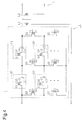
- the circuit constant variable circuit 1 includes series circuits that are connected in parallel. Each of the series circuits includes the capacitor C1 and the first bidirectional switch Q1 that are connected in series. The circuit constant variable circuit 1 further includes the second bidirectional switch Q2 that is connected in parallel to the series circuits that are connected in parallel.
- the first bidirectional switch Q1 of each series circuit and the second bidirectional switch Q2, which is connected in parallel to the series circuits, are set to each mode so that the capacitance of the circuit constant variable circuit 1, that is, the capacitance (resonant parameter) of the resonant circuit, can be varied.
- the series circuits each including the capacitor C1 and the first bidirectional switch Q1, are connected in parallel.
- the circuit constant variable circuit 1 may include a single series circuit as described in the first embodiment.
- series circuits 20 may each include the capacitor C1 and the first bidirectional switch Q1, and the series circuits 20 may be connected to one another by a third bidirectional switch Q3 so as to form a ladder.
- the circuit constant variable circuit 1 may be used as a resonant circuit of the primary circuit 11.
- the first bidirectional switches Q1 of the series circuits 20 and the third bidirectional switches Q3, which connect the first bidirectional switches Q1 to one another, are set to each mode so that the capacitance of the circuit constant variable circuit 1, that is, the capacitance (resonant parameter) of the resonant circuit, can be varied.
- the circuit constant variable circuit 1 is used as a resonant circuit of the primary circuit 11. Instead, the circuit constant variable circuit 1 may be used as a resonant circuit of the secondary circuit 12.
- the circuit constant variable circuit 1 of each of the embodiments includes the capacitor C1 serving as a passive element.
- the capacitor C1 may be replaced with a coil that serves as a passive element. This allows the virtual inductance (circuit constant) of a single coil to be continuously variable within a wide range. Further, the virtual inductance (circuit constant) of the coil can be varied with a simple structure that controls the first and second bidirectional switches Q1 and Q2.
- the passive element may include a capacitor and a coil, and the capacitor and the coil may be connected in series or parallel. Even in this case, the capacitance (circuit constant) of the capacitor and the capacitance (circuit constant) of the coil can be varied.
- the first and second bidirectional switches Q1 and Q2 each include a nitrogen gallium (Gan) bidirectional switching device having a double-gate that includes the first gate terminal G1 and the second gate terminal G2.
- Gan nitrogen gallium
- the bidirectional switches Q1 and Q2 may each include two series circuits, and each of the two series circuits may include a diode D1 and an insulated-gate bipolar transistor Qa (IGBT) that are connected in series.
- the two series circuits are connected in parallel so that the two series circuits have polarities of different directions.
- the bidirectional switches Q1 and Q2 may each include an N-channel power MOS transistor Qx1 and a P-channel power MOS transistor Qx2 that are connected in series.
Landscapes
- Engineering & Computer Science (AREA)
- Power Engineering (AREA)
- Electronic Switches (AREA)
- Dc-Dc Converters (AREA)
Applications Claiming Priority (2)
| Application Number | Priority Date | Filing Date | Title |
|---|---|---|---|
| JP2014001269A JP6406623B2 (ja) | 2014-01-07 | 2014-01-07 | 回路定数可変回路 |
| PCT/JP2014/006409 WO2015104769A1 (ja) | 2014-01-07 | 2014-12-23 | 回路定数可変回路 |
Publications (2)
| Publication Number | Publication Date |
|---|---|
| EP3093988A1 true EP3093988A1 (de) | 2016-11-16 |
| EP3093988A4 EP3093988A4 (de) | 2017-02-15 |
Family
ID=53523626
Family Applications (1)
| Application Number | Title | Priority Date | Filing Date |
|---|---|---|---|
| EP14877881.4A Withdrawn EP3093988A4 (de) | 2014-01-07 | 2014-12-23 | Schaltung mit konstantem variablem schaltkreis |
Country Status (4)
| Country | Link |
|---|---|
| US (1) | US20160322967A1 (de) |
| EP (1) | EP3093988A4 (de) |
| JP (1) | JP6406623B2 (de) |
| WO (1) | WO2015104769A1 (de) |
Cited By (1)
| Publication number | Priority date | Publication date | Assignee | Title |
|---|---|---|---|---|
| US20230396244A1 (en) * | 2022-06-03 | 2023-12-07 | Psemi Corporation | Methods and devices for fast switching of radio frequency switches |
Families Citing this family (4)
| Publication number | Priority date | Publication date | Assignee | Title |
|---|---|---|---|---|
| CN107852102B (zh) * | 2015-07-21 | 2020-04-03 | 三菱电机株式会社 | 电力变换装置 |
| JP6531026B2 (ja) * | 2015-10-20 | 2019-06-12 | 株式会社 日立パワーデバイス | 電力変換装置 |
| US10224806B1 (en) | 2017-11-16 | 2019-03-05 | Infineon Technologies Austria Ag | Power converter with selective transformer winding input |
| US10432097B2 (en) * | 2017-11-30 | 2019-10-01 | Infineon Technologies Austria Ag | Selection control for transformer winding input in a power converter |
Family Cites Families (10)
| Publication number | Priority date | Publication date | Assignee | Title |
|---|---|---|---|---|
| JP4882266B2 (ja) * | 2005-04-12 | 2012-02-22 | 富士電機株式会社 | 交流−交流変換装置 |
| GB2457410B (en) * | 2007-06-22 | 2012-01-04 | Panasonic Corp | Plasma display panel driving device and plasma display |
| JP2012048986A (ja) * | 2010-08-26 | 2012-03-08 | Panasonic Electric Works Co Ltd | 放電灯点灯装置及びそれを用いる照明器具 |
| WO2012026134A1 (ja) * | 2010-08-27 | 2012-03-01 | 三洋電機株式会社 | 電源装置およびそれを用いた電力変換装置 |
| US20120068548A1 (en) * | 2010-09-16 | 2012-03-22 | Advantest Corporation | Wireless power supply apparatus |
| JP5592738B2 (ja) | 2010-09-21 | 2014-09-17 | パナソニック株式会社 | 共振型双方向コンバータ回路 |
| WO2013057896A1 (ja) * | 2011-10-18 | 2013-04-25 | 株式会社アドバンテスト | ワイヤレス受電装置、ワイヤレス給電装置およびワイヤレス給電システム |
| CN102522911B (zh) * | 2011-11-25 | 2014-04-30 | 华为技术有限公司 | 逆变装置及应用其的太阳能光伏并网系统 |
| JP5868304B2 (ja) * | 2012-10-18 | 2016-02-24 | 株式会社アドバンテスト | ワイヤレス受電装置およびそれに利用可能なインピーダンス制御回路、インピーダンス制御方法 |
| JP5715613B2 (ja) * | 2012-12-04 | 2015-05-07 | 株式会社アドバンテスト | ワイヤレス送電システムの中継器およびそれを用いたワイヤレス送電システム |
-
2014
- 2014-01-07 JP JP2014001269A patent/JP6406623B2/ja not_active Expired - Fee Related
- 2014-12-23 WO PCT/JP2014/006409 patent/WO2015104769A1/ja not_active Ceased
- 2014-12-23 US US15/108,823 patent/US20160322967A1/en not_active Abandoned
- 2014-12-23 EP EP14877881.4A patent/EP3093988A4/de not_active Withdrawn
Cited By (2)
| Publication number | Priority date | Publication date | Assignee | Title |
|---|---|---|---|---|
| US20230396244A1 (en) * | 2022-06-03 | 2023-12-07 | Psemi Corporation | Methods and devices for fast switching of radio frequency switches |
| US20250132756A1 (en) * | 2022-06-03 | 2025-04-24 | Psemi Corporation | Methods and devices for fast switching of radio frequency switches |
Also Published As
| Publication number | Publication date |
|---|---|
| JP6406623B2 (ja) | 2018-10-17 |
| EP3093988A4 (de) | 2017-02-15 |
| JP2015130750A (ja) | 2015-07-16 |
| WO2015104769A1 (ja) | 2015-07-16 |
| US20160322967A1 (en) | 2016-11-03 |
Similar Documents
| Publication | Publication Date | Title |
|---|---|---|
| US10714979B2 (en) | Wireless power receiving terminal and wireless charging system | |
| US20150108848A1 (en) | Antenna resonance frequency control driver | |
| US10336201B2 (en) | Contactless power transmission system | |
| US11495995B2 (en) | Advanced overvoltage protection strategy for wireless power transfer | |
| CN106208401B (zh) | 无线充电系统及其控制方法 | |
| US8587973B2 (en) | Internal high-voltage current source in an AC/DC power converter | |
| US10944293B2 (en) | Noncontact power supply apparatus | |
| EP3093988A1 (de) | Schaltung mit konstantem variablem schaltkreis | |
| TW201325009A (zh) | 送電裝置、受電裝置、非接觸式電力傳送系統、及在非接觸式電力傳送系統的送電電力之控制方法 | |
| CN109716637A (zh) | 用于隔离dc-dc转换器的电流保护集成变压器驱动器 | |
| CN112448484B (zh) | 非接触供电装置 | |
| CN109039080A (zh) | 用于控制同步整流器设备的电路和方法 | |
| US11121648B2 (en) | Piezoelectric generator | |
| KR20130050365A (ko) | 수전 장치 및 그것을 이용한 비접촉 전력 전송 시스템 | |
| US8854850B2 (en) | AC power supply apparatus | |
| US10250074B2 (en) | Power supply system | |
| US11283344B2 (en) | Current in-rush limiter | |
| JP2017123699A (ja) | 非接触給電装置及びそれを用いた非接触給電システム | |
| EP2961056A1 (de) | Wechselstromstromquellenvorrichtung | |
| CN112448482B (zh) | 非接触供电装置及送电装置 | |
| US10158280B2 (en) | Signal generation circuit | |
| JP2019054349A (ja) | ゲート駆動回路、および、パワースイッチングシステム | |
| CN111886776A (zh) | 谐振匹配电路 | |
| US7911809B2 (en) | Switching power supply circuit | |
| JP2014176045A (ja) | 半導体リレーの駆動装置及びそれを用いた半導体リレー |
Legal Events
| Date | Code | Title | Description |
|---|---|---|---|
| PUAI | Public reference made under article 153(3) epc to a published international application that has entered the european phase |
Free format text: ORIGINAL CODE: 0009012 |
|
| 17P | Request for examination filed |
Effective date: 20160707 |
|
| AK | Designated contracting states |
Kind code of ref document: A1 Designated state(s): AL AT BE BG CH CY CZ DE DK EE ES FI FR GB GR HR HU IE IS IT LI LT LU LV MC MK MT NL NO PL PT RO RS SE SI SK SM TR |
|
| AX | Request for extension of the european patent |
Extension state: BA ME |
|
| A4 | Supplementary search report drawn up and despatched |
Effective date: 20170118 |
|
| RAP1 | Party data changed (applicant data changed or rights of an application transferred) |
Owner name: PANASONIC INTELLECTUAL PROPERTY MANAGEMENT CO., LT |
|
| RIC1 | Information provided on ipc code assigned before grant |
Ipc: H02M 1/00 20070101ALN20170112BHEP Ipc: H02M 7/48 20070101ALN20170112BHEP Ipc: H02M 3/335 20060101AFI20170112BHEP |
|
| DAX | Request for extension of the european patent (deleted) | ||
| STAA | Information on the status of an ep patent application or granted ep patent |
Free format text: STATUS: THE APPLICATION HAS BEEN WITHDRAWN |
|
| 18W | Application withdrawn |
Effective date: 20180314 |