EP3096200A1 - Procede et dispositif de generation d'un signal d'evenement et systeme de commande industriel - Google Patents
Procede et dispositif de generation d'un signal d'evenement et systeme de commande industriel Download PDFInfo
- Publication number
- EP3096200A1 EP3096200A1 EP15168811.6A EP15168811A EP3096200A1 EP 3096200 A1 EP3096200 A1 EP 3096200A1 EP 15168811 A EP15168811 A EP 15168811A EP 3096200 A1 EP3096200 A1 EP 3096200A1
- Authority
- EP
- European Patent Office
- Prior art keywords
- value
- clock
- signal
- event
- time
- Prior art date
- Legal status (The legal status is an assumption and is not a legal conclusion. Google has not performed a legal analysis and makes no representation as to the accuracy of the status listed.)
- Withdrawn
Links
Images


Classifications
-
- G—PHYSICS
- G06—COMPUTING OR CALCULATING; COUNTING
- G06F—ELECTRIC DIGITAL DATA PROCESSING
- G06F1/00—Details not covered by groups G06F3/00 - G06F13/00 and G06F21/00
- G06F1/04—Generating or distributing clock signals or signals derived directly therefrom
- G06F1/12—Synchronisation of different clock signals provided by a plurality of clock generators
-
- G—PHYSICS
- G06—COMPUTING OR CALCULATING; COUNTING
- G06F—ELECTRIC DIGITAL DATA PROCESSING
- G06F1/00—Details not covered by groups G06F3/00 - G06F13/00 and G06F21/00
- G06F1/04—Generating or distributing clock signals or signals derived directly therefrom
- G06F1/06—Clock generators producing several clock signals
-
- G—PHYSICS
- G06—COMPUTING OR CALCULATING; COUNTING
- G06F—ELECTRIC DIGITAL DATA PROCESSING
- G06F1/00—Details not covered by groups G06F3/00 - G06F13/00 and G06F21/00
- G06F1/04—Generating or distributing clock signals or signals derived directly therefrom
- G06F1/14—Time supervision arrangements, e.g. real time clock
Definitions
- a desired minimization of the time shift should preferably not be too fast, a maximum rate of change in frequency, for example, specified externally, preferably is currently working at 5 ppm per second.
- the system time is preferably to be regarded as a global system time.
- incrementing and decrementing is to be understood as follows. If it is incremented, for example started with zero, then the starting value is loaded, at which point the counter should start again from zero. When decrementing, the counter is loaded at zero crossing with the value which it then decrements again.
- the method is used for use in industrial communication for the operation of isochronous applications.
- a particularly advantageous embodiment of the method provides that the values: start value, end value and signal clock in the context of a fieldbus configuration by means of an engineering system for an isochronous data exchange are specified.
- the temporal independence of a single application or a single device it is particularly advantageous if in case of failure of the system clock this is detected by the method and the generation of the event signal is also without synchronization of the clock source with the system clock, where Returning the system clock the clock source is synchronized again without interrupting the generation of the event signal.
- the respective application or device thus remains unaffected if the communicatively controlled time (system time) fails / returns.
- sideband signals have been used to transmit the required events from the communication to the application.
- a clock source is provided according to the method, which can specify a time for itself, but still can be synchronized with a system clock.
- a plurality of event signals are generated, wherein for the generation of the further event signals cyclic comparisons of further values of further signal clocks with the current value of the counter register are carried out and in the event that the current value of the counter register has reached the value of one of the signal clocks, the corresponding event signal is generated at the time of reaching.
- cyclic comparisons of further values of further signal clocks with the current value of the counter register are carried out and in the event that the current value of the counter register has reached the value of one of the signal clocks, the corresponding event signal is generated at the time of reaching.
- the object mentioned above is also achieved by a device.
- the device for generating an event signal on the one hand a synchronization part, with an input for reading a time of a system clock in a system clock memory, a clock source with a controllable count clock, a counter register, configured to load a start value and the start value with Incrementally incrementing or decrementing the clock source, a tester configured to check whether the current value of the counter register has reached a final value, and in the event that the end value is reached, load the system clock memory to load the current one Time of the system clock output, a divisional means designed to determine a possibly resulting between the system clock and the clock source time shift by a residual division, wherein the start value is the divisor and the dividend is the time in the system clock memory, a compensation means configured in the event that the Remaining division egg The nonzero shift results in controlling the clock source such that in future remainder division after the final value is reached again, the shift is minimized, and second, the device has a signal portion configured
- the device is designed with a programming interface, wherein memory areas for the values start value, end value and signal clock are present, which can be parameterized in the context of a fieldbus configuration by means of an engineering system via the programming interface.
- the device is a stand-alone time generation system, it is preferably designed to detect a system clock failure and to continue generation of the event signal without synchronizing the clock source with the system clock, and when the system clock returns, the clock source is re-synchronized without interrupting the generation of the event signal.
- the device has a plurality of comparison units, which are configured to each continuously perform a comparison of the current value of the counter register with a corresponding associated value of a signal clock, further configured with the respective time of reaching the respective value of the signal Clock to generate a respective event signal, further comprising a plurality of outputs for outputting the respective event signal.
- the object mentioned at the outset is solved by an industrial control system in which a plurality of functional systems have to be synchronized with one another.
- the industrial control system has a device according to one of claims 6 to 9, wherein at least one functional system is designed as an input / output peripheral component for industrial process values and further configured by a connected output with the aid of the event signal to the process values certain times.
- FIG. 1 is a device 1 for generating a plurality of event signals 21,22,23, .., 2n shown.
- the device 1 has a synchronization part 50 and a signal part 51.
- the synchronization part 50 has an input 2 for reading a time of a system clock 100 into a system clock memory 7 and a clock source 3 with a controllable counting clock 4 and a controllable counting step 5.
- the clock source 3 can be regarded as a separate clock for the device 1 and is such designed to be a controllable time / clock source for applications connected via outputs I1, I2, .., In.
- the device 1 has a counter register 6, which is designed to load a start value 10 and incrementally increment or decrement the start value 10 with the aid of the clock source 3.
- a test means 8 is configured to check whether the current value of the counter register 6 has reached a final value 10a and, in the event that the end value 10a has been reached, to issue a load instruction 9 to the system clock memory 7 for loading the current time of the system clock 100.
- the device has a dividing means 40.
- the dividing means 40 is configured to allow a time shift between a system clock 100 and the clock source 3 by a residual division where the seed 10 is the divisor and the dividend is the time in the system clock memory 7.
- the device 1 comprises a compensation means 41, which is designed to control the clock source 3 in such a way that the residual division results in a nonzero shift in a future residual division after a new reaching the final value 10a, the shift is minimized.
- the compensation means 41 has an output for compensation data K for this purpose.
- This compensation data K can be received by the clock source 3, and it can be controlled by the "time" of the clock source 3, for example, the count clock 4 or the count step 5 is adjusted.
- the signal part 51 is configured, via a first output I1, a second output 12, a third output 13, .. up to an n-th output In a first event signal 21, a second event signal 22, a third event Signal 23, .. up to an n-th event signal 2n.
- a comparison unit 11, 12, 13,..., 1n is present in each case.
- the first comparison unit 11 is configured to continuously perform a comparison of the current value of the counter register 6 with a value of a first signal clock 31, furthermore, the first comparison unit 11 is configured with the time of reaching the value of the first signal clock 31, the first event To generate signal 21.
- the second comparison unit 12 is configured to continuously perform a comparison of the current value of the counter register 6 with a value of a second signal clock 32, and also configured with the time of reaching the value of the second signal clock 32, the second event signal 22 to produce.
- the third comparison unit 13 to the n-th comparison unit 1n are configured similarly.
- the values for the different signal clocks 31,32,33, .., 3n are stored in a first memory area 11a, a second memory area 12a, a third memory area 13a, .. up to an n-th memory area 1na.
- the memory areas 11a, 12a, 13a, .., 1na are preferably located in the respective comparison units 11,..., 1n.
- the device 1 has a programming interface 102.
- the values mentioned can be parameterized by means of an engineering system 101 via the programming interface 102.
- the apparatus has a means configured to detect a failure of the system clock 100 and to continue the generation of the event signals even without synchronizing the clock source with the system clock 100, and when the system clock 100 returns, the clock source 3 is resynchronizable without interrupting the generation of the event signals.
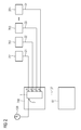
- the device 1 is shown in an embodiment for a processor chip 200.
- the processor module 200 has the task of operating a first application 201, a second application 202, a third application 203, up to an nth application 20n and supplying it with data, in which case the applications must run synchronized with one another.
- the processor module 200 receives the system time via the system clock 100, wherein in the device 1 from the system time on the one hand a separate clock is synchronized, the own clock in the device 1 corresponds to the clock source 3 and on the other different event signals 21, .. , 2n are generated with different clocks for the different applications.
- the processor module 200 with its integrated device 1 can be parameterized via the programming interface 102.
- the FIG. 3 shows an industrial control system 300, such as a programmable logic controller (PLC).
- the industrial control system 300 is configured, for example, as a system on chip (SoC).
- SoC system on chip
- the industrial control system 300 includes several functional systems.
- a first functional system 300 for example embodied as GPIO's of the SoC
- a second functional system 302 configured for example as an input / output peripheral component for onboard inputs and outputs of the PLC
- a third functional system 303 for example designed as a first fieldbus component for a PROFIBus Communication
- a fourth functional system 304 for example configured as a second fieldbus module for a PROFINet communication
- a fifth functional system 305 for example designed as the actual processor core.
- nth functional system 30n Other functional systems, such as an nth functional system 30n, are conceivable, so the industrial control system 300 could be configured as having a plurality of processor cores.
- the industrial control system 300 comprises the already known device 1.
- the device 1 is in turn connected to a system clock 100 and has the already known outputs I1, I2, I3, I4, I5, .., In for the provision of the corresponding event signals.
- the first functional system 301 receives the first event signal 21 in the form of a signal clock 31
- the second functional system 302 receives a second event signal 22 in the form of a second signal clock 32, etc.
- the device 1 By the invention of the device 1 and the connection of the device 1 to a higher system time precisely synchronized, performant connected SPS'n and / or motion controllers on a multi-chip platform, such as a SoC possible.
Landscapes
- Engineering & Computer Science (AREA)
- Theoretical Computer Science (AREA)
- Physics & Mathematics (AREA)
- General Engineering & Computer Science (AREA)
- General Physics & Mathematics (AREA)
- Hardware Redundancy (AREA)
Priority Applications (1)
| Application Number | Priority Date | Filing Date | Title |
|---|---|---|---|
| EP15168811.6A EP3096200A1 (fr) | 2015-05-22 | 2015-05-22 | Procede et dispositif de generation d'un signal d'evenement et systeme de commande industriel |
Applications Claiming Priority (1)
| Application Number | Priority Date | Filing Date | Title |
|---|---|---|---|
| EP15168811.6A EP3096200A1 (fr) | 2015-05-22 | 2015-05-22 | Procede et dispositif de generation d'un signal d'evenement et systeme de commande industriel |
Publications (1)
| Publication Number | Publication Date |
|---|---|
| EP3096200A1 true EP3096200A1 (fr) | 2016-11-23 |
Family
ID=53442464
Family Applications (1)
| Application Number | Title | Priority Date | Filing Date |
|---|---|---|---|
| EP15168811.6A Withdrawn EP3096200A1 (fr) | 2015-05-22 | 2015-05-22 | Procede et dispositif de generation d'un signal d'evenement et systeme de commande industriel |
Country Status (1)
| Country | Link |
|---|---|
| EP (1) | EP3096200A1 (fr) |
Citations (2)
| Publication number | Priority date | Publication date | Assignee | Title |
|---|---|---|---|---|
| US20040156462A1 (en) * | 2001-03-15 | 2004-08-12 | Thomas Fuehrer | Method and device for synchronizing at least one node of a bus system and a corresponding bus system |
| US7475002B1 (en) * | 2004-02-18 | 2009-01-06 | Vmware, Inc. | Method and apparatus for emulating multiple virtual timers in a virtual computer system when the virtual timers fall behind the real time of a physical computer system |
-
2015
- 2015-05-22 EP EP15168811.6A patent/EP3096200A1/fr not_active Withdrawn
Patent Citations (2)
| Publication number | Priority date | Publication date | Assignee | Title |
|---|---|---|---|---|
| US20040156462A1 (en) * | 2001-03-15 | 2004-08-12 | Thomas Fuehrer | Method and device for synchronizing at least one node of a bus system and a corresponding bus system |
| US7475002B1 (en) * | 2004-02-18 | 2009-01-06 | Vmware, Inc. | Method and apparatus for emulating multiple virtual timers in a virtual computer system when the virtual timers fall behind the real time of a physical computer system |
Similar Documents
| Publication | Publication Date | Title |
|---|---|---|
| DE10223723B4 (de) | Ereigniserfassungssystem für eine Folge von Ereignissen und Verfahren zum Erkennen von Ereignissen in einem Prozesssteuerungssystem | |
| EP2718776B1 (fr) | Procédé et système de simulation d'un processus de travail d'une machine-outil | |
| EP2621193B1 (fr) | Dispositif de transmission de données de capteur | |
| EP2067081B1 (fr) | Procédé destiné à la synchronisation de deux dispositifs de commande et dispositif d'automatisation monté de manière redondante | |
| DE19755516A1 (de) | Messeinrichtung für die Flüssigkeits- und/oder Gasanalyse und/oder für die Messung von Feuchte in Flüssigkeiten und/oder Gasen | |
| EP2085848B1 (fr) | Dispositif de traitement et procédé de traitement destinés au traitement d'objets à l'aide d'une mesure temporelle | |
| EP2857913A1 (fr) | Système d'automatisation redondant | |
| DE102014213245A1 (de) | Verfahren zum Verarbeiten von Daten für eine Fahrfunktion eines Fahrzeuges | |
| EP0993698A1 (fr) | Dispositif et procede d'exploitation decentralisee ou de realisation d'une regulation de synchronisme conforme dans un systeme d'entrainement a plusieurs moteurs | |
| EP3214512A1 (fr) | Systeme de commande redondant pour un actionneur et son procede de commande redondant | |
| EP1253494B1 (fr) | Système de commande et/ou de régulation comportant un bus de terrain | |
| DE102008001999A1 (de) | Offsetkompensationsschaltung und damit ausgestatteter Drehratensensor | |
| EP1064589B1 (fr) | Procede de synchronisation d'une base de temps locale sur une base de temps centrale, dispositif correspondant et utilisations preferees | |
| WO2021063932A1 (fr) | Unité d'entrée/sortie pour la capture de données dans un système de bus de terrain | |
| EP2434360B1 (fr) | Système de contrôle de mouvement | |
| EP3267272B1 (fr) | Procédé et dispositif de transmission de données | |
| EP3096200A1 (fr) | Procede et dispositif de generation d'un signal d'evenement et systeme de commande industriel | |
| EP3143506B1 (fr) | Procédé et système permettant d'attribuer une autorisation de commande à un ordinateur | |
| DE10208791C5 (de) | Druckmaschinenantriebssystem | |
| EP3035000A1 (fr) | Dispositif et procede de verification d'un signal de travail d'un dispositif de mesure de position | |
| EP1692578B1 (fr) | Unite peripherique d'un systeme de commande redondant | |
| EP3548975A1 (fr) | Commande d'un processus technique avec une installation à plusieurs noyaux de calcul | |
| EP2980661A1 (fr) | Appareil de commande électronique | |
| EP2434357B1 (fr) | Système d'enregistrement de données technologiques et/ou d'événements du programme | |
| DE102006045022A1 (de) | Anordnung mit Vakuumgerät und Verfahren zu derem Betrieb |
Legal Events
| Date | Code | Title | Description |
|---|---|---|---|
| PUAI | Public reference made under article 153(3) epc to a published international application that has entered the european phase |
Free format text: ORIGINAL CODE: 0009012 |
|
| AK | Designated contracting states |
Kind code of ref document: A1 Designated state(s): AL AT BE BG CH CY CZ DE DK EE ES FI FR GB GR HR HU IE IS IT LI LT LU LV MC MK MT NL NO PL PT RO RS SE SI SK SM TR |
|
| AX | Request for extension of the european patent |
Extension state: BA ME |
|
| RAP1 | Party data changed (applicant data changed or rights of an application transferred) |
Owner name: SIEMENS AKTIENGESELLSCHAFT |
|
| STAA | Information on the status of an ep patent application or granted ep patent |
Free format text: STATUS: THE APPLICATION IS DEEMED TO BE WITHDRAWN |
|
| 18D | Application deemed to be withdrawn |
Effective date: 20170524 |