EP3096394A2 - Filtres haute frequence comprenant des substrats dielectriques destines a transmettre des modes tm dans une direction transversale - Google Patents
Filtres haute frequence comprenant des substrats dielectriques destines a transmettre des modes tm dans une direction transversale Download PDFInfo
- Publication number
- EP3096394A2 EP3096394A2 EP16166149.1A EP16166149A EP3096394A2 EP 3096394 A2 EP3096394 A2 EP 3096394A2 EP 16166149 A EP16166149 A EP 16166149A EP 3096394 A2 EP3096394 A2 EP 3096394A2
- Authority
- EP
- European Patent Office
- Prior art keywords
- resonator
- dielectric
- frequency filter
- signal line
- resonators
- Prior art date
- Legal status (The legal status is an assumption and is not a legal conclusion. Google has not performed a legal analysis and makes no representation as to the accuracy of the status listed.)
- Granted
Links
Images




Classifications
-
- H—ELECTRICITY
- H01—ELECTRIC ELEMENTS
- H01P—WAVEGUIDES; RESONATORS, LINES, OR OTHER DEVICES OF THE WAVEGUIDE TYPE
- H01P1/00—Auxiliary devices
- H01P1/20—Frequency-selective devices, e.g. filters
- H01P1/207—Hollow waveguide filters
- H01P1/208—Cascaded cavities; Cascaded resonators inside a hollow waveguide structure
-
- H—ELECTRICITY
- H01—ELECTRIC ELEMENTS
- H01P—WAVEGUIDES; RESONATORS, LINES, OR OTHER DEVICES OF THE WAVEGUIDE TYPE
- H01P1/00—Auxiliary devices
- H01P1/20—Frequency-selective devices, e.g. filters
- H01P1/207—Hollow waveguide filters
- H01P1/208—Cascaded cavities; Cascaded resonators inside a hollow waveguide structure
- H01P1/2084—Cascaded cavities; Cascaded resonators inside a hollow waveguide structure with dielectric resonators
-
- H—ELECTRICITY
- H01—ELECTRIC ELEMENTS
- H01P—WAVEGUIDES; RESONATORS, LINES, OR OTHER DEVICES OF THE WAVEGUIDE TYPE
- H01P1/00—Auxiliary devices
- H01P1/20—Frequency-selective devices, e.g. filters
- H01P1/201—Filters for transverse electromagnetic waves
- H01P1/202—Coaxial filters
-
- H—ELECTRICITY
- H01—ELECTRIC ELEMENTS
- H01P—WAVEGUIDES; RESONATORS, LINES, OR OTHER DEVICES OF THE WAVEGUIDE TYPE
- H01P5/00—Coupling devices of the waveguide type
- H01P5/02—Coupling devices of the waveguide type with invariable factor of coupling
-
- H—ELECTRICITY
- H01—ELECTRIC ELEMENTS
- H01P—WAVEGUIDES; RESONATORS, LINES, OR OTHER DEVICES OF THE WAVEGUIDE TYPE
- H01P5/00—Coupling devices of the waveguide type
- H01P5/02—Coupling devices of the waveguide type with invariable factor of coupling
- H01P5/022—Transitions between lines of the same kind and shape, but with different dimensions
-
- H—ELECTRICITY
- H01—ELECTRIC ELEMENTS
- H01P—WAVEGUIDES; RESONATORS, LINES, OR OTHER DEVICES OF THE WAVEGUIDE TYPE
- H01P5/00—Coupling devices of the waveguide type
- H01P5/08—Coupling devices of the waveguide type for linking dissimilar lines or devices
- H01P5/10—Coupling devices of the waveguide type for linking dissimilar lines or devices for coupling balanced lines or devices with unbalanced lines or devices
- H01P5/103—Hollow-waveguide/coaxial-line transitions
-
- H—ELECTRICITY
- H01—ELECTRIC ELEMENTS
- H01P—WAVEGUIDES; RESONATORS, LINES, OR OTHER DEVICES OF THE WAVEGUIDE TYPE
- H01P7/00—Resonators of the waveguide type
- H01P7/04—Coaxial resonators
-
- H—ELECTRICITY
- H01—ELECTRIC ELEMENTS
- H01P—WAVEGUIDES; RESONATORS, LINES, OR OTHER DEVICES OF THE WAVEGUIDE TYPE
- H01P7/00—Resonators of the waveguide type
- H01P7/06—Cavity resonators
-
- H—ELECTRICITY
- H01—ELECTRIC ELEMENTS
- H01P—WAVEGUIDES; RESONATORS, LINES, OR OTHER DEVICES OF THE WAVEGUIDE TYPE
- H01P7/00—Resonators of the waveguide type
- H01P7/10—Dielectric resonators
Definitions
- the invention relates to a high frequency filter, which is particularly suitable for the transmission of TM modes in the transverse direction.
- TM modes or TM waves
- only the electric field has components in the propagation direction and the magnetic fields are located only in the plane perpendicular to the direction of propagation.
- TM waves are therefore also known as e-waves.
- a high-frequency filter which comprises a plurality of resonator chambers, which are connected to one another via openings.
- each resonator chamber are a dielectric material and an inner conductor, wherein the inner conductor is formed integrally with the housing.
- About a feed conductor of the inner conductor is excited, via which also the dielectric material is excited.
- a disadvantage of this high-frequency filter is the complex construction, which necessarily results in larger deviations in the filter properties in production.
- a disadvantage of this structure is that an increased space requirement is required in order to realize the desired filter properties.
- the resonator can be constructed very compact. Furthermore, very good filtering results are achieved because the signal line connection directly excites the dielectric in contact therewith. This excitation does not take place indirectly in that the TM wave first propagates in the cavity of the resonator and possibly also excites an inner conductor, via which the dielectric is then excited to oscillate.
- the first signal line terminal and / or the second signal line terminal in the area in which they are in contact with the first and / or nth dielectric and / or the first and / or n-1 th separator, perpendicular to the surface of the Separating device, or parallel to a central axis, which passes through the high-frequency filter and all resonator chambers arranged.
- the first signal line connection which engages in the recess or in the continuous recess of the dielectric in the resonator of the first resonator, is in contact with this dielectric or is arranged without contact to this dielectric.
- the second signal line connection is lower, but the assembly is easier.
- the method according to the invention for balancing the high-frequency filter comprises various method steps.
- a method step all coupling openings of the 1 + X-th separation device and / or the n-1-X-th separation device are closed at the beginning, wherein X is 0 at the beginning.
- a reflection parameter at the first signal line connection and / or a further reflection parameter at the second signal line connection are measured.
- the resonance frequency and / or the coupling bandwidth or the coupling bandwidth are set to a desired value. With this method, the resonance frequency and / or the coupling bandwidth of a resonator chamber be set to the desired value regardless of other resonator chambers.
- a further advantage is provided if one or both end faces of each of the n-dielectrics are coated with a metal layer, this metal layer then representing one of the n-1 separation devices, and wherein at least one recess within the metal layer forms the at least one coupling opening.
- the filter can be made very compact. Between the inserts, the n-1 separators can then be located. The lateral peripheral surfaces of the inserts, as well as the lateral peripheral surface of the n-1 separators, then form in the embodiment c) the peripheral wall of the housing. In the embodiment b) in which the at least one insert is surrounded by a circumferential housing wall, the high-frequency filter is constructed very stable.
- a further advantage of the high-frequency filter according to the invention also exists if a diameter of at least one resonator chamber is defined and / or specified by at least one insert, in particular by an annular insert which is based on the housing wall. This allows the resonance frequency to be adjusted.
- the particular form-fitting leaning of the insert on the housing wall also ensures that the insert is not displaced over time in its position.
- At least one anti-rotation element between at least one of the n-1 separating devices and the at least one insert and / or the adjacent dielectric is attached, which prevents the mutual rotation of these elements. It is also possible that at least one anti-rotation element between the housing bottom and / or the housing cover and / or the housing wall and the insert in the first resonator and the n-th resonator chamber is mounted, which prevents the mutual rotation of these elements. This ensures that the resonance frequencies and the group delay of the individual resonators do not change over time due to vibrations of the high-frequency filter.
- Another advantage of the high-frequency filter according to the invention is when the inserts of at least two not directly adjacent n-resonators have an opening, wherein the at least two openings are interconnected by a channel, for example, at least partially within the housing wall runs.
- a channel runs an electrical conductor, wherein the electrical conductor capacitively and / or inductively couples the two resonators.
- the n-type dielectrics may be disc-shaped, or all or some of the n-type dielectrics may differ completely or partially in their dimensions. It is also possible for all or at least one of the n dielectrics to completely or partially fill the volume of their respective resonator chamber. Due to the geometric design and the arrangement of the dielectrics, the behavior of each resonator with respect to its resonator frequency and its coupling bandwidth can be adjusted accordingly.
- the coupling between the individual resonators is thereby increased in that the dielectric in the first resonator is in contact with the first isolator and the dielectric in the nth resonator is in contact with the n-th th separator, the remaining dielectrics of the remaining n-2 resonators being connected to both which are in contact with respective resonator chamber bounding separators. It is particularly advantageous if, in addition, the dielectric in the first resonator is additionally in contact with the housing cover and the dielectric in the nth resonator is in contact with the housing bottom. By the word "in contact”, it is understood that at least two entities touch each other.
- the dielectrics of the n resonators are preferably firmly connected to the respective separating device or the respective separating devices, whereby the coupling is improved.
- Another advantage of the high-frequency filter according to the invention is also that the arrangement and / or the size and / or the cross-sectional shape of at least one coupling opening of one of the n-1 separation devices completely or partially to the arrangement and / or the size and / or the cross-sectional shape of a Coupling opening of a different one of the n-1 separators. It is also possible that the number of coupling openings in the n-1 separation devices completely or partially different from each other. As a result, the coupling between the individual resonators can be set to the desired value.
- each resonator chamber may have at least one additional opening to the outside of the housing, wherein at least one tuning element can be introduced into the resonator chamber via this additional opening.
- the distance between the tuning element inserted through the at least one additional opening in the resonator chamber may be changed to the corresponding respective dielectric within the resonator chamber.
- a plurality of tuning elements can be introduced into a resonator, wherein, for example, a tuning element consists entirely of a metal or a metallic coating, whereas the other tuning element comprises a dielectric material.
- the tuning element, which consists of a metallic material can be coarse tuning and the tuning element comprising a dielectric material used for fine tuning the resonant frequency and / or the coupling bandwidth of the corresponding resonator.
- the distance between the at least one spacer element and the respective dielectric within the resonator chamber can also be reduced to such an extent that it is in direct contact with it.
- the dielectric of each resonator chamber may also have a recess, wherein the distance between the tuning element and the dielectric is reduced such that the tuning element dips into the recess of the respective dielectric and thus is in contact therewith.
- the tuning element occurs in this case in particular perpendicular to the signal transmission direction in the resonator chamber.
- the method according to the invention for adjusting the high-frequency filter is repeated accordingly for the remaining resonator chambers.
- the resonant frequency and / or the coupling bandwidth of the first and / or last that is to say the nth resonator is set to the desired value
- the value of the counter variable X is increased by 1.
- the previous process steps are executed again. Again, a reflection factor at the first signal line connection and / or a reflection factor at the second signal line connection are measured.
- the tuning of the high-frequency filter starts at the resonators, in which engage the signal line terminals, ie at the outermost resonators, and ends at the resonator or at the resonators which are arranged in the center of the high-frequency filter.
- the resonator in the center of the high-frequency filter must be used once for the measurement of the reflection factor at the first signal line connection and at another time for the measurement of the reflection factor at the second signal line connection.
- the coupling openings of the two separating devices, which surround the resonator in the center of the high-frequency filter, must be closed depending on the measurement of the respective reflection factor to the other signal line connection out.
- the forward transmission factor and / or the backward transmission factor can be measured in addition to the reflection factors at the first signal line connection and / or at the second signal line connection.
- the resonance frequencies and / or the coupling bandwidths can be changed for each resonator by changing the diameter of the resonator chamber, which is possible, for example, by exchanging the at least one insert for another insert with changed dimensions. It may also be the arrangement and / or the number and / or the size and / or the Cross-sectional shape of the at least one coupling opening by turning and / or replacing the at least one separating device to be changed.
- the screwing in or turning out of at least one tuning element into at least one resonator chamber likewise makes it possible to change the resonant frequency and / or the coupling bandwidth.
- the dielectric in the resonator chamber can be replaced by another dielectric with changed dimensions.
- FIG. 1 shows an embodiment of the high-frequency filter 1 according to the invention in an exploded view.
- the high-frequency filter 1 according to the invention comprises a housing 2 which has a housing bottom 3 and a housing cover 4 spaced from the housing bottom 3 and a housing wall 5 encircling the housing bottom 3 and the housing cover 4.
- Both the housing cover 4, as well as the housing bottom 3 have at least one opening, via which a signal line connection 30 1 , 30 2 , as will be shown later, can be introduced.
- a first signal line connection 30 1 is fed through the opening of the housing cover 4 to the high-frequency filter 1 and a second signal line connection 30 2 through the opening in the housing bottom 3.
- the openings in the housing cover 4 and in the housing bottom 3 need not in the center of the housing bottom 3 or the housing cover. 4 be arranged. It is also possible that the openings are arranged eccentrically. Preferably, both the housing cover 4, and the housing cover 3 opposite the housing cover 4 can be removed. In the assembled state of the high-frequency filter 1 the housing cover 4 and the housing bottom 3 are preferably screwed to the circumferential housing wall 5.
- the high-frequency filter 1 also has a plurality of resonators 6 1 , 6 2 ,..., 6 n , wherein each of the n resonators 6 1 , 6 2 ,..., 6 n has at least one resonator chamber 7 1 , 7 2 , ..., 7 n includes.
- N is a natural number ⁇ 1.
- each resonator 7 1, 7 2, ..., 7 n is at least one dielectric 8 1, 8 2, ..., 8 n.
- This dielectric 8 1 , 8 2 ,..., 8 n is preferably disk-shaped or cylindrical. It extends over the entire volume of the respective resonator chamber 7 1 , 7 2 ,..., 7 n or only over a part thereof.
- the individual resonator 7 1, 7 2, ..., 7 n are by separation devices 9 1, 9 2, ... 9 n-1 separated from each other.
- These separating devices 9 1 , 9 2 ,... 9 n-1 are preferably cutting discs.
- These separators 9 1 , 9 2 , ..., 9 n-1 are made of an electrically conductive material or are coated with such.
- Each of these separating devices 9 1 , 9 2 ,..., 9 n-1 has at least one coupling opening 10.
- the size, the geometric shape, the number and the arrangement of the coupling opening 10 within the respective separating device 9 1 , 9 2 , ..., 9 n-1 can be chosen arbitrarily and by separating device 9 1 , 9 2 , ...
- the diameter of the coupling openings 10 is, depending on the frequency range, for example, only a fraction of a millimeter. It can be several millimeters, especially at low frequencies.
- the separators 9 1 , 9 2 ,..., 9 n-1 are preferably thinner than the dielectrics 8 1 , 8 2 , ..., 8 n .
- the separating devices 9 1 , 9 2 ,..., 9 n-1 are preferably only a few millimeters thick, preferably they are thinner than 3 millimeters, more preferably they are thinner than 2 millimeters.
- the separating devices 9 1 , 9 2 ,..., 9 n-1 and the housing 2 are each formed as separate separate components.
- the separating devices 9 1 , 9 2 ,..., 9 n-1 are completely surrounded by the circumferential housing wall 5 of the high-frequency filter 1 in the mounted state of the high-frequency filter 1 and are arranged only and exclusively inside the high-frequency filter 1. They are preferably not screwed to the housing 2.
- the separating devices 9 1 , 9 2 ,..., 9 n-1 can be inserted into the housing cover 4 and / or the housing bottom 3 when the cover 4 is open. This means that they do not constitute part of the outer wall of the high-frequency filter 1.
- the separating devices 9 1 , 9 2 ,..., 9 n-1 rest on the respective dielectrics 8 1 , 8 2 ,..., 8 n and are preferably supported exclusively on the housing bottom 3 and / or on the housing cover 4 of the high-frequency filter 1 from.
- Each resonator chamber 7 1 , 7 2 ,..., 7 n can also comprise at least one insert 11 1 , 11 2 ,..., 11 n .
- Such an insert 11 1 , 11 2 ,..., 11 n is preferably a ring which, with its outer surface, preferably bears in a form-fitting manner against an inner surface of the housing wall 5.
- Such an insert 11 1 , 11 2 ,..., 11 n which is electrically conductive, can be used for adjusting the volume of the resonator chamber 7 1 , 7 2 ,..., 7 n and thus for adjusting the resonant frequency.
- the housing 2 of the high-frequency filter 1 is preferably kept free of internal conductors, which are galvanically connected to the housing 2 at one end.
- FIG. 1 In addition, a central axis 12 is shown, which passes through the high-frequency filter 1.
- the signal transmission direction 21 corresponds to the central axis 12.
- the resonators 6 1 , 6 2 ,..., 6 n are arranged one above the other. Therefore, each resonator 6 1, 6 2, ..., 6 n maximum of two directly adjacent resonators 6 1, 6 2, ..., 6 n, wherein the resonators 6 1, 6 2, ..., 6 n from each other, are separated by the respective separation means 9 1 , 9 2 , ..., 9 n-1 .
- a coupling of the individual resonators 6 1 , 6 2 ,..., 6 n is only possible via the respective coupling openings 10 within the separating devices 9 1 , 9 2 ,..., 9 n-1 .
- the coupling of the individual resonators 6 1 , 6 2 ,..., 6 n takes place parallel or predominantly parallel to the signal transmission direction 21.
- the H field 20 propagates perpendicular or with a component predominantly perpendicular to the signal transmission direction 21.
- All resonators 6 1 , 6 2 ,..., 6 n are penetrated by the central axis 12.
- the central axis 12 is perpendicular to the end face of the respective dielectrics 8 1 , 8 2 , ..., 8 n .
- the inner wall of the housing 5 of the high-frequency filter 1 is preferably cylindrical in cross-section.
- Other shapes in cross section are also possible.
- FIG. 2 is a diagram explaining that a magnetic field 20 (H field) is disposed perpendicular to the signal transmission direction 21. As shown in FIG. The magnetic field lines thereby propagate radially outward about the signal transmission direction 21.
- the central axis 12 and the signal transmission direction 21 are preferably congruent.
- FIG. 3 shows a longitudinal section through the high-frequency filter 1 according to the invention, which shows a plurality of resonators 6 1 , 6 2 , ..., 6 n with the respective resonator chambers 7 1 , 7 2 , ..., 7 n , via coupling openings 10 in the separators.
- 9 1 , 9 2 , ..., 9 n-1 are interconnected.
- a first signal line connection 30 1 is passed through an opening in the housing cover 4.
- a second signal line connection 30 2 is passed through an opening in the housing bottom 3.
- the openings in the housing cover 4 and in the housing bottom 3 are preferably arranged centrally. An off-center arrangement is also possible.
- the first signal line terminal 30 1 contacts an end face of the first dielectric 8 1 .
- the first dielectric 8 1 is excited directly by the first signal line terminal 30. 1
- the first signal line connection 30 1 is therefore in contact with the first dielectric 8 1 .
- the end face of the first dielectric 8 1 is not in contact with the housing cover 4 in this exemplary embodiment, which means that the end face 8 1 does not touch the housing cover 4.
- the second signal line connection 30 2 also touches an end face of the n-th dielectric 8 n , and is in contact with this.
- the nth dielectric 8 n is excited directly by the second signal line connection 30 2 .
- the end face of the n-th dielectric does not touch the housing bottom 3, so it is not in contact with this.
- Each resonator 6 1 , 6 2 , 6 3 , 6 4 , ..., 6 n each having a resonator 7 1 , 7 2 , 7 3 , 7 4 , ..., 7 n possess.
- Each resonator 6 1 , 6 2 , 6 3 , 6 4 ,..., 6 n is separated by a separator 9 1 , 9 2 , 9 3 ,..., 9 n-1 from the other resonators 6 1 , 6 2 , 6 3 , 6 4 , ..., 6 n separately.
- Each resonator 6 1 , 6 2 , 6 3 , 6 4 ,..., 6 n comprises a dielectric 8 1 , 8 2 , 8 3 , 8 4 ,..., 8 n .
- the signal line terminals 30 1 and 30 2 are arranged on different, in particular on opposite sides of the housing 2 at this.
- the first signal line connection 30 1 penetrates the housing cover 4 and the second signal line connection 30 2 passes through the housing bottom 3 or vice versa.
- the dielectrics 8 1 , 8 2 , 8 3 , 8 4 ,..., 8 n can all be made of the same material. It is also possible that only some of the dielectrics 8 1 , 8 2 , 8 3 , 8 4 ,..., 8 n are made of the same material and other dielectrics 8 1 , 8 2 , 8 3 , 8 4 , .. ., 8n of a different material. It is also possible to form all dielectrics 8 1 , 8 2 , 8 3 , 8 4 ,..., 8 n from different materials.
- FIG. 3 fill the individual dielectrics 8 1, 8 2, ..., 8 n, the volume of each resonator 7 1, 7 2, ..., 7 n are not completely.
- the dielectrics 8 1 , 8 2 , ..., 8 n point in this embodiment the same dimensions with respect to their respective height and their respective diameter.
- the inserts 11 1 , 11 2 , 11 3 , 11 4 , ..., 11 n all have the same outer diameter. Their wall thickness, so the inner diameter is different, however. This means that the volume of the individual resonator chambers 7 1 , 7 2 ,..., 7 n is different.
- the electrically conductive housing cover 4 is both in electrical contact with a front side of the housing 5, as well with an end face of the first insert 11 1 .
- the housing bottom 3 is also in electrical contact with the housing 5 and an end face of the nth insert 11 n .
- the housing 5 may be electrically conductive, that is, for example, may be made of metal, but not necessarily.
- the housing 5 can be made of any other material, in particular of an electrically non-conductive material such as a dielectric or plastic.
- the function of the housing 5 is to mechanically hold together and mechanically fix the components located in the interior of the housing 5.
- the housing 5 can only consist of a dielectric, if it is ensured that the resonator chambers 7 1 , 7 2 ,..., 7 n are shielded from the surroundings of the high-frequency filter 1. Such shielding can for example be done by the inserts 11 1 , 11 2 , ..., 11 n .
- the separating devices 9 1 , 9 2 ,..., 9 n-1 have an outer diameter, which preferably has an inner diameter the housing wall 5 corresponds. This means that an outer surface, ie a circumferential wall of each separating device 9 1 , 9 2 ,..., 9 n-1 touches the inner surface of the housing 5, ie is in mechanical contact therewith.
- the coupling openings 10 of a separating device 9 1 , 9 2 ,..., 9 n-1 may differ from the coupling openings of the other separating devices 9 1 , 9 2 ,..., 9 n-1 with respect to their arrangement, ie orientation and / or their number and / or their size and / or their cross-sectional shape.
- the coupling openings 10 of the individual separation devices 9 1 , 9 2 ,..., 9 n-1 have a different diameter and are arranged, for example, at different locations of the separation devices 9 1 , 9 2 ,..., 9 n-1 .
- the coupling openings 10 connect the individual resonator chambers 7 1 , 7 2 ,..., 7 n to one another, wherein on the one hand they depend on the free volume of a resonator 6 1 , 6 2 ,..., 6 n or on the dielectric 8 1 , 8 2 , ..., 8 n of the resonator 6 1 , 6 2 , ..., 6 n are surrounded.
- An electrically conductive insert 11 1 , 11 2 ,..., 11 n can not cover a coupling opening 10. It is also possible that the cross-sectional shape of the individual coupling openings 10 changes over the length, that is, over the height. Between the individual separation devices 9 1, 9 2, ..., 9 n-1 and the inserts 11 1, 11 2, ..., 11 n typically is no cavity. The same applies preferably also to the first insert 11 1 and the housing cover 4, as well as to the nth insert 11 n and the housing bottom 3.
- the dielectrics 8 1 , 8 2 , ..., 8 n are also in contact with their respective separator 9 1 , 9 2 ,..., 9 n-1 .
- the dielectrics 8 1 , 8 2 ,..., 8 n can be pressed and / or soldered to the respective separating devices 9 1 , 9 2 ,..., 9 n-1 .
- the inserts 11 1 , 11 2 , ..., 11 n with the corresponding separating devices 9 1 , 9 2 , ..., 9 n-1 pressed together form-fitting and / or soldered.
- a rotation of the individual elements is prevented from each other, whereby the electrical properties of the high-frequency filter 1 does not change over a longer period.
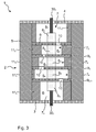
- FIG. 4 shows a longitudinal section through a further embodiment of the high-frequency filter according to the invention 1.
- the first dielectric 8 1 is on its front side in contact with the housing cover 4. A distance between the first dielectric 8 1 and the housing cover 4 is not present.
- the same applies to the n-th dielectric 8 n which is also in contact with the housing bottom 3 with its front side. A distance between the n-th dielectric 8 n and the housing bottom 3 is not present.
- the elements of the high-frequency filter 1 are preferably pressed together. This pressing manifests itself, for example, in that the individual dielectrics 8 1 , 8 2 ,..., 8 n partially protrude into the individual separating devices 9 1 , 9 2 ,..., 9 n-1 .
- the high-frequency filter 1 also has a plurality of tuning elements 40 1 , 40 2 , 40 3 , 40 4 ,..., 40 n .
- At least one tuning element 40 1 , 40 2 ,..., 40 n is inserted into the resonator chamber 7 1 through an additional opening 41 1 , 41 2 , 41 3 , 41 4 ,. 7 2 , ..., 7 n of at least one of the n-resonators 6 1 , 6 2 , ... 6 n introduced.
- the openings 41 1 , 41 2 ,..., 41 n extend through the housing wall 5 and through the corresponding insert 11 1 , 11 2 ,..., 11 n into the resonator chamber 7 1 , 7 2 ,. 7 n inside.
- the corresponding tuning element 41 1, 41 2, ..., 41 n may then into the respective resonator 7 1, 7 2, ..., 7 n into or be unscrewed.
- the distance between the tuning element 41 1 , 41 2 ,..., 41 n and the respective dielectric 8 1 , 8 2 ,..., 8 n is variable.
- the respective opening 41 1 , 41 2 ,..., 41 n preferably runs perpendicular to the signal propagation direction 21 and thus likewise perpendicular to the central axis 12.
- the first dielectric 8 1 in the first resonator 6 1 has a depression into which the first signal line 30 1 protrudes. This increases the coupling.
- the first signal line 30 1 is preferably in contact with the dielectric 8 1 . However, it would also be possible for the first signal line 30 1 to be arranged without contact with the first dielectric 8 1 in the latter. The same applies to the nth dielectric 8 n n in the nth resonator. 6
- the recess may be centrally or eccentrically attached to the dielectric 8 1 , 8 n .
- FIG. 5 shows a longitudinal section through a further embodiment of the high-frequency filter 1 according to the invention.
- the dielectric 8 1 in the first resonator chamber 7 1 has a continuous recess, through which the first signal line 30 1 extends.
- the first signal line 30 1 comes directly into contact with the first separator 9 first
- the second signal line connection 30 2 which extends through a continuous recess in the n-th dielectric 8 n of the n-th resonator 6 n and is in contact with the n-1 th separator 9 n-1 .
- the respective signal line terminals 30 1 , 30 2 are also in contact with the respective dielectric 8 1 , 8 n , which is penetrated by them. However, they could also be arranged without contact to these.
- the continuous recess may be mounted centrally or off-center on the dielectric 8 1 , 8 n .
- the part of the signal line connection 30 1 , 30 2 which is in contact with the respective dielectric 8 1 , 8 n or with the respective separating device 9 1 , 9 n-1 , runs parallel to the central axis 12, or parallel to the signal transmission direction 21 other parts of the signal line connection 30 1 , 30 2 do not have to run parallel to the signal transmission direction 21 or to the central axis 12.
- those parts of the two signal line connections 30 1 , 30 2 run parallel to the signal transmission direction 21, which are located within the first or n-th resonator chamber 7 1 , 7 n .
- the second dielectric 8 2 in the second resonator chamber 7 2 also has a recess, so that a second tuning element 40 2 can dip into the second dielectric 8 2 .
- the inserts 11 1 , 11 2 ,..., 11 n of at least two resonators 6 1 , 6 2 ,..., 6 n which are not directly adjacent to one another have an opening 50 1 , 50 2 .
- the at least two openings 50 1 , 50 2 are interconnected by a channel 51, this channel 51 preferably being parallel to the signal propagation direction 21, ie parallel to the central axis 12.
- This channel 51 extends at least partially within the housing wall 5. It is also possible that this channel extends completely within the housing wall 5. It is also possible that this channel does not run within the housing wall 5, but only through the inserts 11 1 , 11 2 , ..., 11 n and the separating devices 9 1 , 9 2 ,..., 9 n lying between them. 1 .
- This electrical conductor 52 couples the at least two resonators 6 1 , 6 n capacitively and / or inductively with each other.
- a first end 53 1 of the electrical conductor 52 is connected to the first separator 9 1 .
- the first end 53 1 of the electrical conductor 52 preferably runs parallel to the signal propagation direction 21 and thus parallel to the central axis 12.
- a second end 53 2 of the electrical conductor 52 is galvanically connected to the n-1 th separator 9 n-1 .
- the second end 53 2 also preferably extends parallel to the signal propagation direction 21 and thus parallel to the central axis 12.
- the first and the second end 53 1 , 53 2 can with the respective separation devices 9 1 , 9 2 , ...
- the electrical conductor 52 which extends within the channel 51, is within this preferably via dielectric spacers, not shown, of the walls which surround the channel 51, electrically separated and held by these in its position.
- FIG. 6 shows a longitudinal section through a further embodiment of the high-frequency filter according to the invention 1.
- a first cross-coupling occurs between the first resonator 6 1 and the n-th resonator 6 n instead.
- An electrical conductor 52 couples these two resonators 6 1 , 6 n together.
- a first end 53 1 of the electrical conductor 52 is connected to the housing cover 4 this time.
- a second over-coupling takes place between the second resonator 6 2 and the fourth resonator 6 4 .
- An electrical conductor 60 couples these two resonators 6 2 , 6 4 together.
- a first end 61 1 of the second electrical conductor 60 is connected to the second separator 9 2 .
- a second end 61 2 of the electrical conductor is connected to the n-1-th separator 9 n-1 . Shown by dashed lines is a possibility that the second end 61 2 of the second electrical conductor 60 could also be connected to the third separator 9 3 .
- the anti-rotation elements 62 may consist of a combination between a projection and a receiving opening.
- the housing cover 4 may have a projection which engages in a corresponding receiving opening within the first insert 11 1 .
- the anti-rotation elements 62 are preferably between at least one of the n-1 separators 9 1 , 9 2 , ..., 9 n and the at least one insert 11 1 , 11 2 , ..., 11 n and / or the adjacent dielectric. 8 1 , 8 2 , ..., 8 n attached.
- a respective anti-rotation element 62 between the housing bottom 3 and / or the housing cover 4 and / or the housing wall 5 and the insert 11 1 in the first resonator chamber 7 1 and the insert 11 n in the n-th resonator chamber 7 n mounted the prevents the mutual rotation of those elements which are arranged closest to the first and / or the second signal line connection 30 1 , 30 2 . This also prevents twisting of those elements which are arranged further inside the high-frequency filter 1.
- the high-frequency filter 1 is preferably realized in stacked construction, wherein all the resonators 6 1 , 6 2 , ..., 6 n are arranged one above the other.
- the anti-rotation elements 62 thereby prevent the electrical properties of the individual resonators 6 1 , 6 2 ,..., 6 n , which include, for example, the resonance frequencies, from changing.
- FIG. 7 shows a longitudinal section through a further embodiment of the high-frequency filter according to the invention 1.
- the individual resonator 7 1 , 7 2 , ..., 7 n are completely filled by the respective dielectric 8 1 , 8 2 , ..., 8 n .
- the height of each dielectric 8 1 , 8 2 , ..., 8 n corresponds to the height of the respective insert 11 1 , 11 2 , ..., 11 n .
- the outer diameter of each dielectric 8 1 , 8 2 ,..., 8 n corresponds approximately to the inner diameter of the respective insert 11 1 , 11 2 ,..., 11 n .
- the dielectric 8 1 , 8 2 , ..., 8 n lies with its peripheral wall on an inner wall of the respective insert 11 1 , 11 2 , ..., 11 n a form-fitting manner.
- FIG. 8 shows a longitudinal section through a further embodiment of the high-frequency filter according to the invention 1.
- the first signal line terminal 30 1 contacts the first dielectric 8 1 off-center.
- the same applies to the second signal line connection 30 2 which contacts the nth dielectric off-center.
- the dielectrics 8 1, 8 2, ..., 8, the volume of their respective resonator 7 1, 7 2, ..., 7 n completely fill n a cross-coupling between two may also not directly adjacent resonators 6 1 , 6 2 , ..., 6 n can be achieved.
- the first dielectric 8 1 and the third dielectric 8 3 that is to say the dielectrics 8 1 , 8 2 ,..., 8 n between their resonators 6 1 , 6 2 ,..., 6 n should take place in the longitudinal direction a preferably continuous slot 80.
- This continuous slot 80 can be introduced, for example, by means of a diamond saw in the existing of a ceramic dielectric 8 1 , 8 2 , ..., 8 n .
- this slot 80 at least the first end 53 1 and the second end 53 2 of the electrical conductor 52 is arranged.
- Figure 9A shows a longitudinal section through a further embodiment of the high-frequency filter according to the invention 1.
- the separator 9 1 , 9 2 , ..., 9 n-1 is an integral part of each dielectrics 8 1 , 8 2 , ..., 8 n .
- This metal layer then represents one of the n-1 separation devices 9 1 , 9 2 ,..., 9 n-1 .
- a recess 90 within the metal layer, ie within the coating, thereby forms a coupling opening 10 between two resonators 6 1 , 6 2 ,..., 6 n .
- Adjacent dielectrics 8 1 , 8 2 ,..., 8 n have the recesses 90 within the coating of the metal layer in each case at the same locations, so that a coupling in the signal propagation direction 21 is possible becomes.
- FIG. 9B shows a modified embodiment of Figure 9A.
- the housing 2 is formed in this case from the inserts 11 1 , 11 2 , ..., 11 n , the housing bottom 3 and the housing cover 4 .
- the inserts 11 1 , 11 2 , ..., 11 n are preferably interconnected by screws 91, which further preferably extend parallel to the central axis 12.
- a complementary or alternative connection by an adhesive or by a soldering and / or welding connection is also possible.
- the inserts 11 1 , 11 2 , ..., 11 n could also be connected to each other by a latching connection without tools.
- a protrusion on the surface of an insert 11 1 , 11 2 ,..., 11 n which (the surface) extends parallel to the housing cover 4 or housing bottom 3, could in an opening of the adjacent insert 11 1 , 11 second , ..., 11 n are introduced, wherein the projection is moved by a rotational movement in the opening such that the inserts 11 1 , 11 2 , ..., 11 n no longer detach from each other when only a force along the central axis 12 is applied.
- the separating means 9 1 , 9 2 ,..., 9 n-1 are not formed in the form of a coating on the dielectrics 8 1 , 8 2 ,..., 8 n , they would be between the inserts 11 1 , 11 2 , ..., 11 n arranged. You could then represent either a part of the outer wall of the housing wall 5 or in a recess of the inserts 11 1 , 11 2 , ..., 11 n , in the area of the inserts 11 1 , 11 2 , ..., 11 n a reduced Thickness, be arranged. In this case, the separating devices 9 1 , 9 2 ,..., 9 n-1 would be invisible from the outside.
- FIG. 10 shows a flowchart which explains how the resonance frequency and / or the coupling bandwidth for a resonator 6 1 , 6 2 , ..., 6 n is set to equalize the high-frequency filter 1 according to the invention.
- a counter variable X is defined with 0.
- method step S 1 is carried out.
- all coupling openings 10 of the 1 + x th separator and / or the n-1 th separator are closed. Looking at the longitudinal section in FIG. 4 this would be the coupling openings 10 in the first separator 9 1 and in the last separator 9 n-1 .
- the method step S 2 is carried out.
- the reflection factor is measured at the first signal line connection 30 1 and / or at the second signal line connection 30 2 .
- the measured reflection factor becomes unique the geometric properties of the first and the nth resonator 6 1 , 6 n determined.
- the step S 3 is executed.
- the resonance frequency and / or the coupling bandwidth of the first and / or the nth resonator 6 1 , 6 n is set to a specific value.
- the method step S 2 is again carried out in order to measure the changed reflection factor again to determine whether the method step S 3 must be repeated, or whether the set values for the resonant frequency and / or the coupling bandwidth already the desired values correspond.
- the tuning of the high-frequency filter 1 according to the invention is carried out from outside to inside, that is to say beginning at the resonators 6 1 , 6 n arranged at the first and / or second signal line terminals 30 1 , 30 2 .
- further resonators 6 2 , 6 3 ,..., 6 n-2 are successively added by opening the respective coupling openings. This process is for example in FIG. 11 described.
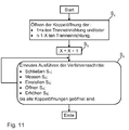
- FIG. 11 shows a further flowchart, which explains how the resonance frequencies and / or the coupling bandwidths for the other resonators 6 2 , 6 3 , ..., 6 n-1 are set to equalize the high-frequency filter 1 according to the invention.
- the method step S 4 is carried out. Within the method step S 4 is at least a coupling opening 10 of the 1 + X-th separator and / or the n-1-X-th separator opened. With regard to FIG. 4 this would be the coupling opening 10 in the separators 9 1 and 9 n-1 .
- the method step S 5 is carried out.
- the value of X is increased by 1.
- the method step S 6 is listed, in which again the method steps S 1 , S 2 , S 3 , S 4 , S 5 are carried out, namely until all coupling openings 10 are opened. This means that subsequent to that FIG. 4 the coupling openings 10 of the separator 9 2 and the coupling openings 10 of the separator 9 3 are closed. Again, the reflection factor at the first signal line connection 30 1 and / or at the second signal line connection 30 2 is measured. Following this, the resonance frequency and / or the coupling bandwidth of the first and the last two resonators 6 1 , 6 2 and 6 n , 6 n-1 is set again.
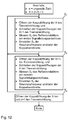
- the resonator 6 3 that is to say the resonator in the middle of the high-frequency filter 1 according to the invention, is used once for the calculation of the reflection factor at the first signal line connection 30 1 and once for the calculation of the reflection factor at the second signal line connection 30 2 in the method for balancing the high-frequency filter 1.
- the coupling openings 10 of the X-th separator are opened and the coupling openings 10 of the X + 1-th separator closed.
- the coupling openings would be opened in the separator 9 2 and closed in the separator 9 3 .
- the reflection factor at the first signal line connection 30 1 is measured and the resonance frequency and / or the coupling bandwidth are adjusted accordingly.
- the coupling opening 10 of the X + 1 th separator is opened and the coupling openings 10 of the X th separator are closed.
- the coupling openings 10 would be closed in the separator 9 2 , whereas the coupling opening 10 would be opened within the separator 9 3 3 .
- method step S 2 is carried out again and the reflection factor at the second signal line connection 30 2 is measured.
- method step S 3 is carried out, in which the resonance frequency and / or the coupling bandwidth are set.
- the resonant frequency and / or the coupling bandwidth of the resonator in the middle of the high-frequency filter 1 according to the invention must be set such that an acceptable value is achieved both for the reflection factor at the first signal line terminal 30 1 and for the reflection factor at the second signal line terminal 30 2 . Possibly. compromises must be made.
- step S 9 is carried out and the coupling openings of the X-th and the X + 1-th separator are opened.
- all coupling openings 10 in all separators 9 1 , 9 2 , ..., 9 n-1 are open. This condition automatically exits after passing through the flowchart FIG. 11 when there are an even number of resonators 6 1 , 6 2 , ..., 6 n .
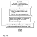
- method step S 10 is carried out.
- the forward transmission factor and / or the backward transmission factor are determined.
- the resonance frequency and / or the coupling bandwidth are again set to a specific value, or finely adjusted. This takes place in method step S 3 .
- Repetition of the method steps S 2 and S 10 is possible as often as the desired target value for the resonant frequency and / or the coupling bandwidth has not yet been reached in method step S 3 .
- FIG. 14 shows a further flowchart, which explains by which measures the resonance frequency and / or the coupling bandwidth within a resonator 6 1 , 6 2 , ..., 6 n can be changed.
- the following method steps can be carried out individually or in combination with one another.
- the method step S 11 describes that the resonance frequency and / or the coupling bandwidth can be adjusted by the diameter of the respective resonator chamber 7 1 , 7 2 ,..., 7 n by exchanging the insert 11 1 , 11 2 , ... , 11 n can be done by another with changed dimensions, in particular with a changed inner diameter.
- the method step S 12 can be carried out.
- an intended separating device 9 1 , 9 2 ,..., 9 n-1 can be rotated so that the coupling openings 10 are arranged differently. It is also possible that the separating device 9 1 , 9 2 , ..., 9 n is replaced by another, wherein the coupling openings 10, a different arrangement and / or a different number and / or a different size and / or another Have geometry.
- the method step S 13 can be carried out.
- a change in the resonance frequency and / or the coupling bandwidth can also be achieved by further screwing and / or turning at least one tuning element 40 1 , 40 2 ,..., 40 n into the respective resonator chamber 7 1 , 7 2 , n take place.
- a resonator chamber 7 1 , 7 2 , ..., 7 n and more than one tuning element 40 1 , 40 2 , ..., 40 n can be turned on or turned off.
- the method step S 14 can also be carried out.
- at least one dielectric 8 1 , 8 2 ,..., 8 n in a resonator chamber 7 1 , 7 2 ,..., 7 n can be replaced by another dielectric 8 1 , 8 2 ,. 8 n exchanged, which has changed dimensions, in particular in its height and / or its diameter.
- step S 1 or each time when coupling openings 10 are to be closed, this is preferably done by the respective separation device 9 1 , 9 2 , ... 9 n is replaced by one which has no coupling openings 10.
Landscapes
- Physics & Mathematics (AREA)
- Electromagnetism (AREA)
- Control Of Motors That Do Not Use Commutators (AREA)
Applications Claiming Priority (1)
| Application Number | Priority Date | Filing Date | Title |
|---|---|---|---|
| DE102015005523.2A DE102015005523B4 (de) | 2015-04-30 | 2015-04-30 | Hochfrequenzfilter mit dielektrischen Substraten zur Übertragung von TM-Moden in transversaler Richtung |
Publications (3)
| Publication Number | Publication Date |
|---|---|
| EP3096394A2 true EP3096394A2 (fr) | 2016-11-23 |
| EP3096394A3 EP3096394A3 (fr) | 2017-03-01 |
| EP3096394B1 EP3096394B1 (fr) | 2019-06-12 |
Family
ID=55794902
Family Applications (1)
| Application Number | Title | Priority Date | Filing Date |
|---|---|---|---|
| EP16166149.1A Active EP3096394B1 (fr) | 2015-04-30 | 2016-04-20 | Filtres haute frequence comprenant des substrats dielectriques destines a transmettre des modes tm dans une direction transversale |
Country Status (5)
| Country | Link |
|---|---|
| US (1) | US10211501B2 (fr) |
| EP (1) | EP3096394B1 (fr) |
| CN (1) | CN106099282B (fr) |
| DE (1) | DE102015005523B4 (fr) |
| ES (1) | ES2742507T3 (fr) |
Families Citing this family (5)
| Publication number | Priority date | Publication date | Assignee | Title |
|---|---|---|---|---|
| EP3583656B1 (fr) * | 2017-02-15 | 2021-12-15 | Isotek Microwave Limited | Résonateur à micro-ondes, filtre à micro-ondes et multiplexeur à micro-ondes |
| EP3502771B1 (fr) * | 2017-12-19 | 2023-06-07 | Qubig GmbH | Modulateur électro-optique |
| GB2573381B (en) * | 2018-03-16 | 2022-07-20 | Isotek Microwave Ltd | A microwave resonator, a microwave filter and a microwave multiplexer |
| CN113036327B (zh) * | 2021-03-25 | 2022-04-15 | 南通大学 | 一种基于双模介质谐振器的异频双通道滤波巴伦 |
| WO2025174276A1 (fr) * | 2024-02-12 | 2025-08-21 | Telefonaktiebolaget Lm Ericsson (Publ) | Procédé et unité de filtre de signal pour commander la perte d'énergie dans un dispositif sans fil dans un réseau sans fil |
Citations (1)
| Publication number | Priority date | Publication date | Assignee | Title |
|---|---|---|---|---|
| US6549092B1 (en) | 1999-10-04 | 2003-04-15 | Murata Manufacturing Co. Ltd. | Resonator device, filter, composite filter device, duplexer, and communication device |
Family Cites Families (19)
| Publication number | Priority date | Publication date | Assignee | Title |
|---|---|---|---|---|
| US4267537A (en) | 1979-04-30 | 1981-05-12 | Communications Satellite Corporation | Right circular cylindrical sector cavity filter |
| US4721933A (en) * | 1986-09-02 | 1988-01-26 | Hughes Aircraft Company | Dual mode waveguide filter employing coupling element for asymmetric response |
| CA1251835A (fr) | 1988-04-05 | 1989-03-28 | Wai-Cheung Tang | Multiplexeur a resonateurs images dielectriques |
| JP3309610B2 (ja) | 1994-12-15 | 2002-07-29 | 株式会社村田製作所 | 誘電体共振器装置 |
| US5576674A (en) | 1995-03-17 | 1996-11-19 | Allen Telecom Group, Incorporated | Optimum, multiple signal path, multiple-mode filters and method for making same |
| JP3019750B2 (ja) | 1995-08-21 | 2000-03-13 | 株式会社村田製作所 | 誘電体共振器装置 |
| JP3405140B2 (ja) * | 1996-12-11 | 2003-05-12 | 株式会社村田製作所 | 誘電体共振器 |
| JP3298485B2 (ja) | 1997-02-03 | 2002-07-02 | 株式会社村田製作所 | 多重モード誘電体共振器 |
| DE19847006A1 (de) | 1998-10-13 | 2000-04-20 | Degussa | Ruß |
| AUPP747098A0 (en) | 1998-12-04 | 1998-12-24 | Alcatel | Waveguide directional filter |
| CA2313925A1 (fr) * | 2000-07-17 | 2002-01-17 | Mitec Telecom Inc. | Filtre passe-bande accordable |
| FR2815475B1 (fr) * | 2000-10-18 | 2003-01-17 | Thomson Multimedia Sa | Filtre en guide d'onde |
| US6624723B2 (en) | 2001-07-10 | 2003-09-23 | Radio Frequency Systems, Inc. | Multi-channel frequency multiplexer with small dimension |
| DE102006061141B4 (de) * | 2006-12-22 | 2014-12-11 | Kathrein-Werke Kg | Hochfrequenzfilter mit Sperrkreiskopplung |
| CN201369378Y (zh) * | 2008-12-26 | 2009-12-23 | 成都赛纳赛德科技有限公司 | 窄带fss滤波器 |
| CN201466182U (zh) * | 2009-05-12 | 2010-05-12 | 成都赛纳赛德科技有限公司 | 紧凑型自谐振膜片滤波器 |
| FR2996395B1 (fr) | 2012-10-01 | 2015-08-14 | Centre Nat Etd Spatiales | Dispositif routeur multiports compact |
| CN103855448A (zh) * | 2012-12-03 | 2014-06-11 | 武汉凡谷电子技术股份有限公司 | Tm模介质滤波器 |
| GB201303024D0 (en) | 2013-02-21 | 2013-04-03 | Mesaplexx Pty Ltd | Filter |
-
2015
- 2015-04-30 DE DE102015005523.2A patent/DE102015005523B4/de not_active Expired - Fee Related
-
2016
- 2016-04-20 EP EP16166149.1A patent/EP3096394B1/fr active Active
- 2016-04-20 ES ES16166149T patent/ES2742507T3/es active Active
- 2016-04-29 US US15/142,364 patent/US10211501B2/en active Active
- 2016-04-29 CN CN201610279931.9A patent/CN106099282B/zh active Active
Patent Citations (1)
| Publication number | Priority date | Publication date | Assignee | Title |
|---|---|---|---|---|
| US6549092B1 (en) | 1999-10-04 | 2003-04-15 | Murata Manufacturing Co. Ltd. | Resonator device, filter, composite filter device, duplexer, and communication device |
Also Published As
| Publication number | Publication date |
|---|---|
| EP3096394A3 (fr) | 2017-03-01 |
| EP3096394B1 (fr) | 2019-06-12 |
| ES2742507T3 (es) | 2020-02-14 |
| US10211501B2 (en) | 2019-02-19 |
| CN106099282B (zh) | 2020-06-05 |
| DE102015005523B4 (de) | 2018-03-29 |
| US20160322688A1 (en) | 2016-11-03 |
| CN106099282A (zh) | 2016-11-09 |
| DE102015005523A1 (de) | 2016-11-03 |
Similar Documents
| Publication | Publication Date | Title |
|---|---|---|
| EP3089260B1 (fr) | Filtres multiples comprenant des substrats dielectriques destines a transmettre des modes tm dans une direction transversale | |
| DE2538614C3 (de) | Dielektrischer Resonator | |
| DE69424618T2 (de) | Dielektrischer Resonator, dielektrisches Bandsperrfilter und dielektrisches Filter | |
| EP2656435B1 (fr) | Filtre haute fréquence réglable | |
| EP3096394B1 (fr) | Filtres haute frequence comprenant des substrats dielectriques destines a transmettre des modes tm dans une direction transversale | |
| DE2723040A1 (de) | Dielektrischer resonator | |
| EP3220473A1 (fr) | Filtre coaxial en treillis | |
| EP2912714B1 (fr) | Filtre réglable à haute fréquence | |
| DE102017100926A1 (de) | Hohlraumfilter mit keramischem Resonator | |
| DE2726799C2 (de) | Frequenzweiche | |
| EP3451441B1 (fr) | Filtre coaxial | |
| DE69729030T2 (de) | Dielektrische Mehrschichtvorrichtung und dazugehöriges Herstellungsverfahren | |
| DE3236664C2 (fr) | ||
| DE69712802T2 (de) | Dielektrisches Filter | |
| DE69116306T2 (de) | Kopplungsstruktur für einen dielektrischen Filter | |
| DE2705245C2 (fr) | ||
| DE2746376C2 (de) | Koppelvorrichtung zwischen einer Koaxialleitung und einem Hohlleiter | |
| DE69321152T2 (de) | Dielektrischer Resonator und Verfahren zum Justieren seiner Charakteristik | |
| EP3298649B1 (fr) | Système de transmission des hautes fréquences comprenant une traversée hf reliée par ligne | |
| DE69425235T2 (de) | Dielektrischer Resonator und Herstellunsverfahren dafür | |
| DE19526583A1 (de) | Dielektrisches Filter | |
| EP2991158B1 (fr) | Filtre de gaine generique | |
| DE19842040B4 (de) | Dielektrisches Filter | |
| DE19842218B4 (de) | Dielektrisches Filter | |
| EP4233124B1 (fr) | Ensemble filtre de fer à gaufres pour signaux haute fréquence |
Legal Events
| Date | Code | Title | Description |
|---|---|---|---|
| PUAI | Public reference made under article 153(3) epc to a published international application that has entered the european phase |
Free format text: ORIGINAL CODE: 0009012 |
|
| AK | Designated contracting states |
Kind code of ref document: A2 Designated state(s): AL AT BE BG CH CY CZ DE DK EE ES FI FR GB GR HR HU IE IS IT LI LT LU LV MC MK MT NL NO PL PT RO RS SE SI SK SM TR |
|
| AX | Request for extension of the european patent |
Extension state: BA ME |
|
| PUAL | Search report despatched |
Free format text: ORIGINAL CODE: 0009013 |
|
| AK | Designated contracting states |
Kind code of ref document: A3 Designated state(s): AL AT BE BG CH CY CZ DE DK EE ES FI FR GB GR HR HU IE IS IT LI LT LU LV MC MK MT NL NO PL PT RO RS SE SI SK SM TR |
|
| AX | Request for extension of the european patent |
Extension state: BA ME |
|
| RIC1 | Information provided on ipc code assigned before grant |
Ipc: H01P 1/208 20060101AFI20170120BHEP |
|
| STAA | Information on the status of an ep patent application or granted ep patent |
Free format text: STATUS: REQUEST FOR EXAMINATION WAS MADE |
|
| 17P | Request for examination filed |
Effective date: 20170829 |
|
| RBV | Designated contracting states (corrected) |
Designated state(s): AL AT BE BG CH CY CZ DE DK EE ES FI FR GB GR HR HU IE IS IT LI LT LU LV MC MK MT NL NO PL PT RO RS SE SI SK SM TR |
|
| STAA | Information on the status of an ep patent application or granted ep patent |
Free format text: STATUS: EXAMINATION IS IN PROGRESS |
|
| 17Q | First examination report despatched |
Effective date: 20171108 |
|
| GRAP | Despatch of communication of intention to grant a patent |
Free format text: ORIGINAL CODE: EPIDOSNIGR1 |
|
| STAA | Information on the status of an ep patent application or granted ep patent |
Free format text: STATUS: GRANT OF PATENT IS INTENDED |
|
| RIC1 | Information provided on ipc code assigned before grant |
Ipc: H01P 7/06 20060101ALN20181113BHEP Ipc: H01P 5/103 20060101ALI20181113BHEP Ipc: H01P 1/208 20060101AFI20181113BHEP Ipc: H01P 7/10 20060101ALN20181113BHEP |
|
| RIC1 | Information provided on ipc code assigned before grant |
Ipc: H01P 7/10 20060101ALN20181120BHEP Ipc: H01P 1/208 20060101AFI20181120BHEP Ipc: H01P 7/06 20060101ALN20181120BHEP Ipc: H01P 5/103 20060101ALI20181120BHEP |
|
| INTG | Intention to grant announced |
Effective date: 20181218 |
|
| RAP1 | Party data changed (applicant data changed or rights of an application transferred) |
Owner name: KATHREIN SE |
|
| GRAS | Grant fee paid |
Free format text: ORIGINAL CODE: EPIDOSNIGR3 |
|
| GRAA | (expected) grant |
Free format text: ORIGINAL CODE: 0009210 |
|
| STAA | Information on the status of an ep patent application or granted ep patent |
Free format text: STATUS: THE PATENT HAS BEEN GRANTED |
|
| AK | Designated contracting states |
Kind code of ref document: B1 Designated state(s): AL AT BE BG CH CY CZ DE DK EE ES FI FR GB GR HR HU IE IS IT LI LT LU LV MC MK MT NL NO PL PT RO RS SE SI SK SM TR |
|
| REG | Reference to a national code |
Ref country code: GB Ref legal event code: FG4D Free format text: NOT ENGLISH |
|
| REG | Reference to a national code |
Ref country code: CH Ref legal event code: EP |
|
| REG | Reference to a national code |
Ref country code: AT Ref legal event code: REF Ref document number: 1143802 Country of ref document: AT Kind code of ref document: T Effective date: 20190615 |
|
| REG | Reference to a national code |
Ref country code: IE Ref legal event code: FG4D Free format text: LANGUAGE OF EP DOCUMENT: GERMAN |
|
| REG | Reference to a national code |
Ref country code: DE Ref legal event code: R096 Ref document number: 502016004979 Country of ref document: DE |
|
| REG | Reference to a national code |
Ref country code: SE Ref legal event code: TRGR |
|
| REG | Reference to a national code |
Ref country code: NL Ref legal event code: MP Effective date: 20190612 |
|
| REG | Reference to a national code |
Ref country code: LT Ref legal event code: MG4D |
|
| PG25 | Lapsed in a contracting state [announced via postgrant information from national office to epo] |
Ref country code: NO Free format text: LAPSE BECAUSE OF FAILURE TO SUBMIT A TRANSLATION OF THE DESCRIPTION OR TO PAY THE FEE WITHIN THE PRESCRIBED TIME-LIMIT Effective date: 20190912 Ref country code: AL Free format text: LAPSE BECAUSE OF FAILURE TO SUBMIT A TRANSLATION OF THE DESCRIPTION OR TO PAY THE FEE WITHIN THE PRESCRIBED TIME-LIMIT Effective date: 20190612 Ref country code: LT Free format text: LAPSE BECAUSE OF FAILURE TO SUBMIT A TRANSLATION OF THE DESCRIPTION OR TO PAY THE FEE WITHIN THE PRESCRIBED TIME-LIMIT Effective date: 20190612 Ref country code: HR Free format text: LAPSE BECAUSE OF FAILURE TO SUBMIT A TRANSLATION OF THE DESCRIPTION OR TO PAY THE FEE WITHIN THE PRESCRIBED TIME-LIMIT Effective date: 20190612 |
|
| PG25 | Lapsed in a contracting state [announced via postgrant information from national office to epo] |
Ref country code: LV Free format text: LAPSE BECAUSE OF FAILURE TO SUBMIT A TRANSLATION OF THE DESCRIPTION OR TO PAY THE FEE WITHIN THE PRESCRIBED TIME-LIMIT Effective date: 20190612 Ref country code: RS Free format text: LAPSE BECAUSE OF FAILURE TO SUBMIT A TRANSLATION OF THE DESCRIPTION OR TO PAY THE FEE WITHIN THE PRESCRIBED TIME-LIMIT Effective date: 20190612 Ref country code: BG Free format text: LAPSE BECAUSE OF FAILURE TO SUBMIT A TRANSLATION OF THE DESCRIPTION OR TO PAY THE FEE WITHIN THE PRESCRIBED TIME-LIMIT Effective date: 20190912 Ref country code: GR Free format text: LAPSE BECAUSE OF FAILURE TO SUBMIT A TRANSLATION OF THE DESCRIPTION OR TO PAY THE FEE WITHIN THE PRESCRIBED TIME-LIMIT Effective date: 20190913 |
|
| PG25 | Lapsed in a contracting state [announced via postgrant information from national office to epo] |
Ref country code: CZ Free format text: LAPSE BECAUSE OF FAILURE TO SUBMIT A TRANSLATION OF THE DESCRIPTION OR TO PAY THE FEE WITHIN THE PRESCRIBED TIME-LIMIT Effective date: 20190612 Ref country code: EE Free format text: LAPSE BECAUSE OF FAILURE TO SUBMIT A TRANSLATION OF THE DESCRIPTION OR TO PAY THE FEE WITHIN THE PRESCRIBED TIME-LIMIT Effective date: 20190612 Ref country code: SK Free format text: LAPSE BECAUSE OF FAILURE TO SUBMIT A TRANSLATION OF THE DESCRIPTION OR TO PAY THE FEE WITHIN THE PRESCRIBED TIME-LIMIT Effective date: 20190612 Ref country code: NL Free format text: LAPSE BECAUSE OF FAILURE TO SUBMIT A TRANSLATION OF THE DESCRIPTION OR TO PAY THE FEE WITHIN THE PRESCRIBED TIME-LIMIT Effective date: 20190612 Ref country code: RO Free format text: LAPSE BECAUSE OF FAILURE TO SUBMIT A TRANSLATION OF THE DESCRIPTION OR TO PAY THE FEE WITHIN THE PRESCRIBED TIME-LIMIT Effective date: 20190612 Ref country code: PT Free format text: LAPSE BECAUSE OF FAILURE TO SUBMIT A TRANSLATION OF THE DESCRIPTION OR TO PAY THE FEE WITHIN THE PRESCRIBED TIME-LIMIT Effective date: 20191014 |
|
| REG | Reference to a national code |
Ref country code: ES Ref legal event code: FG2A Ref document number: 2742507 Country of ref document: ES Kind code of ref document: T3 Effective date: 20200214 |
|
| PG25 | Lapsed in a contracting state [announced via postgrant information from national office to epo] |
Ref country code: IT Free format text: LAPSE BECAUSE OF FAILURE TO SUBMIT A TRANSLATION OF THE DESCRIPTION OR TO PAY THE FEE WITHIN THE PRESCRIBED TIME-LIMIT Effective date: 20190612 Ref country code: SM Free format text: LAPSE BECAUSE OF FAILURE TO SUBMIT A TRANSLATION OF THE DESCRIPTION OR TO PAY THE FEE WITHIN THE PRESCRIBED TIME-LIMIT Effective date: 20190612 Ref country code: IS Free format text: LAPSE BECAUSE OF FAILURE TO SUBMIT A TRANSLATION OF THE DESCRIPTION OR TO PAY THE FEE WITHIN THE PRESCRIBED TIME-LIMIT Effective date: 20191012 |
|
| REG | Reference to a national code |
Ref country code: DE Ref legal event code: R097 Ref document number: 502016004979 Country of ref document: DE |
|
| REG | Reference to a national code |
Ref country code: DE Ref legal event code: R082 Ref document number: 502016004979 Country of ref document: DE Representative=s name: FLACH BAUER STAHL PATENTANWAELTE PARTNERSCHAFT, DE Ref country code: DE Ref legal event code: R081 Ref document number: 502016004979 Country of ref document: DE Owner name: ERICSSON AB, SE Free format text: FORMER OWNER: KATHREIN SE, 83022 ROSENHEIM, DE Ref country code: DE Ref legal event code: R081 Ref document number: 502016004979 Country of ref document: DE Owner name: TELEFONAKTIEBOLAGET LM ERICSSON (PUBL), SE Free format text: FORMER OWNER: KATHREIN SE, 83022 ROSENHEIM, DE |
|
| PG25 | Lapsed in a contracting state [announced via postgrant information from national office to epo] |
Ref country code: TR Free format text: LAPSE BECAUSE OF FAILURE TO SUBMIT A TRANSLATION OF THE DESCRIPTION OR TO PAY THE FEE WITHIN THE PRESCRIBED TIME-LIMIT Effective date: 20190612 |
|
| PLBE | No opposition filed within time limit |
Free format text: ORIGINAL CODE: 0009261 |
|
| STAA | Information on the status of an ep patent application or granted ep patent |
Free format text: STATUS: NO OPPOSITION FILED WITHIN TIME LIMIT |
|
| PG25 | Lapsed in a contracting state [announced via postgrant information from national office to epo] |
Ref country code: PL Free format text: LAPSE BECAUSE OF FAILURE TO SUBMIT A TRANSLATION OF THE DESCRIPTION OR TO PAY THE FEE WITHIN THE PRESCRIBED TIME-LIMIT Effective date: 20190612 Ref country code: DK Free format text: LAPSE BECAUSE OF FAILURE TO SUBMIT A TRANSLATION OF THE DESCRIPTION OR TO PAY THE FEE WITHIN THE PRESCRIBED TIME-LIMIT Effective date: 20190612 |
|
| REG | Reference to a national code |
Ref country code: DE Ref legal event code: R082 Ref document number: 502016004979 Country of ref document: DE Representative=s name: FLACH BAUER STAHL PATENTANWAELTE PARTNERSCHAFT, DE Ref country code: DE Ref legal event code: R081 Ref document number: 502016004979 Country of ref document: DE Owner name: TELEFONAKTIEBOLAGET LM ERICSSON (PUBL), SE Free format text: FORMER OWNER: ERICSSON AB, STOCKHOLM, SE |
|
| 26N | No opposition filed |
Effective date: 20200313 |
|
| PG25 | Lapsed in a contracting state [announced via postgrant information from national office to epo] |
Ref country code: SI Free format text: LAPSE BECAUSE OF FAILURE TO SUBMIT A TRANSLATION OF THE DESCRIPTION OR TO PAY THE FEE WITHIN THE PRESCRIBED TIME-LIMIT Effective date: 20190612 Ref country code: IS Free format text: LAPSE BECAUSE OF FAILURE TO SUBMIT A TRANSLATION OF THE DESCRIPTION OR TO PAY THE FEE WITHIN THE PRESCRIBED TIME-LIMIT Effective date: 20200224 |
|
| PG2D | Information on lapse in contracting state deleted |
Ref country code: IS |
|
| PG25 | Lapsed in a contracting state [announced via postgrant information from national office to epo] |
Ref country code: MC Free format text: LAPSE BECAUSE OF FAILURE TO SUBMIT A TRANSLATION OF THE DESCRIPTION OR TO PAY THE FEE WITHIN THE PRESCRIBED TIME-LIMIT Effective date: 20190612 |
|
| REG | Reference to a national code |
Ref country code: CH Ref legal event code: PL |
|
| PG25 | Lapsed in a contracting state [announced via postgrant information from national office to epo] |
Ref country code: LI Free format text: LAPSE BECAUSE OF NON-PAYMENT OF DUE FEES Effective date: 20200430 Ref country code: CH Free format text: LAPSE BECAUSE OF NON-PAYMENT OF DUE FEES Effective date: 20200430 Ref country code: LU Free format text: LAPSE BECAUSE OF NON-PAYMENT OF DUE FEES Effective date: 20200420 |
|
| REG | Reference to a national code |
Ref country code: BE Ref legal event code: MM Effective date: 20200430 |
|
| PG25 | Lapsed in a contracting state [announced via postgrant information from national office to epo] |
Ref country code: BE Free format text: LAPSE BECAUSE OF NON-PAYMENT OF DUE FEES Effective date: 20200430 |
|
| GBPC | Gb: european patent ceased through non-payment of renewal fee |
Effective date: 20200420 |
|
| PG25 | Lapsed in a contracting state [announced via postgrant information from national office to epo] |
Ref country code: IE Free format text: LAPSE BECAUSE OF NON-PAYMENT OF DUE FEES Effective date: 20200420 Ref country code: GB Free format text: LAPSE BECAUSE OF NON-PAYMENT OF DUE FEES Effective date: 20200420 |
|
| REG | Reference to a national code |
Ref country code: ES Ref legal event code: PC2A Owner name: ERICSSON AB Effective date: 20210603 |
|
| REG | Reference to a national code |
Ref country code: ES Ref legal event code: PC2A Owner name: TELEFONAKTIEBOLAGET LM ERICSSON (PUBL) Effective date: 20210607 |
|
| REG | Reference to a national code |
Ref country code: FI Ref legal event code: PCE Owner name: TELEFONAKTIEBOLAGET LM ERICSSON (PUBL) |
|
| PG25 | Lapsed in a contracting state [announced via postgrant information from national office to epo] |
Ref country code: MT Free format text: LAPSE BECAUSE OF FAILURE TO SUBMIT A TRANSLATION OF THE DESCRIPTION OR TO PAY THE FEE WITHIN THE PRESCRIBED TIME-LIMIT Effective date: 20190612 Ref country code: CY Free format text: LAPSE BECAUSE OF FAILURE TO SUBMIT A TRANSLATION OF THE DESCRIPTION OR TO PAY THE FEE WITHIN THE PRESCRIBED TIME-LIMIT Effective date: 20190612 |
|
| REG | Reference to a national code |
Ref country code: AT Ref legal event code: MM01 Ref document number: 1143802 Country of ref document: AT Kind code of ref document: T Effective date: 20210420 |
|
| PG25 | Lapsed in a contracting state [announced via postgrant information from national office to epo] |
Ref country code: MK Free format text: LAPSE BECAUSE OF FAILURE TO SUBMIT A TRANSLATION OF THE DESCRIPTION OR TO PAY THE FEE WITHIN THE PRESCRIBED TIME-LIMIT Effective date: 20190612 |
|
| PGFP | Annual fee paid to national office [announced via postgrant information from national office to epo] |
Ref country code: SE Payment date: 20220427 Year of fee payment: 7 Ref country code: FR Payment date: 20220425 Year of fee payment: 7 |
|
| PG25 | Lapsed in a contracting state [announced via postgrant information from national office to epo] |
Ref country code: AT Free format text: LAPSE BECAUSE OF NON-PAYMENT OF DUE FEES Effective date: 20210420 |
|
| PGFP | Annual fee paid to national office [announced via postgrant information from national office to epo] |
Ref country code: FI Payment date: 20220427 Year of fee payment: 7 |
|
| PGFP | Annual fee paid to national office [announced via postgrant information from national office to epo] |
Ref country code: ES Payment date: 20230503 Year of fee payment: 8 |
|
| REG | Reference to a national code |
Ref country code: SE Ref legal event code: EUG |
|
| PG25 | Lapsed in a contracting state [announced via postgrant information from national office to epo] |
Ref country code: SE Free format text: LAPSE BECAUSE OF NON-PAYMENT OF DUE FEES Effective date: 20230421 Ref country code: FR Free format text: LAPSE BECAUSE OF NON-PAYMENT OF DUE FEES Effective date: 20230430 Ref country code: FI Free format text: LAPSE BECAUSE OF NON-PAYMENT OF DUE FEES Effective date: 20230420 |
|
| REG | Reference to a national code |
Ref country code: ES Ref legal event code: FD2A Effective date: 20250530 |
|
| PGFP | Annual fee paid to national office [announced via postgrant information from national office to epo] |
Ref country code: DE Payment date: 20250429 Year of fee payment: 10 |
|
| PG25 | Lapsed in a contracting state [announced via postgrant information from national office to epo] |
Ref country code: ES Free format text: LAPSE BECAUSE OF NON-PAYMENT OF DUE FEES Effective date: 20240421 |