EP3097643B1 - Nichtflüchtiger zähler mit einem ferroelektrischen kondensator - Google Patents
Nichtflüchtiger zähler mit einem ferroelektrischen kondensator Download PDFInfo
- Publication number
- EP3097643B1 EP3097643B1 EP15740718.0A EP15740718A EP3097643B1 EP 3097643 B1 EP3097643 B1 EP 3097643B1 EP 15740718 A EP15740718 A EP 15740718A EP 3097643 B1 EP3097643 B1 EP 3097643B1
- Authority
- EP
- European Patent Office
- Prior art keywords
- count
- stage
- ferroelectric capacitor
- signal
- pulses
- Prior art date
- Legal status (The legal status is an assumption and is not a legal conclusion. Google has not performed a legal analysis and makes no representation as to the accuracy of the status listed.)
- Not-in-force
Links
Images




Classifications
-
- H—ELECTRICITY
- H03—ELECTRONIC CIRCUITRY
- H03K—PULSE TECHNIQUE
- H03K21/00—Details of pulse counters or frequency dividers
- H03K21/08—Output circuits
-
- G—PHYSICS
- G11—INFORMATION STORAGE
- G11C—STATIC STORES
- G11C11/00—Digital stores characterised by the use of particular electric or magnetic storage elements; Storage elements therefor
- G11C11/21—Digital stores characterised by the use of particular electric or magnetic storage elements; Storage elements therefor using electric elements
- G11C11/22—Digital stores characterised by the use of particular electric or magnetic storage elements; Storage elements therefor using electric elements using ferroelectric elements
- G11C11/221—Digital stores characterised by the use of particular electric or magnetic storage elements; Storage elements therefor using electric elements using ferroelectric elements using ferroelectric capacitors
-
- H—ELECTRICITY
- H03—ELECTRONIC CIRCUITRY
- H03K—PULSE TECHNIQUE
- H03K23/00—Pulse counters comprising counting chains; Frequency dividers comprising counting chains
- H03K23/76—Pulse counters comprising counting chains; Frequency dividers comprising counting chains using magnetic cores or ferro-electric capacitors
- H03K23/766—Pulse counters comprising counting chains; Frequency dividers comprising counting chains using magnetic cores or ferro-electric capacitors using thin-film devices
Definitions
- a sensor attached to a door generates a small electrical pulse each time the door is operated.
- a piezoelectric signal generator uses the mechanical energy associated with opening the door to generate an electrical pulse. The designer wishes to count the number of pulses generated over time. During the time in which the counts are accumulating, no electrical power is available to the counter. After some time, the counter can be powered in a separate circuit and the stored count readout. However, the counter must retain the count during the times that no power is available and perform the counting operation using only the power provided by the sensor.
- the present invention is defined by the independent claims 1 and 3.
- the present invention includes a counter having a first count stage.
- the first count stage includes a ferroelectric capacitor characterized by first and second polarization states, a variable impedance element, reset and count ports and a detector.
- the variable impedance element has an impedance between first and second switch terminals that is determined by a signal on a control terminal, the ferroelectric capacitor is connected between the control terminal and the first switch terminal.
- the reset port is configured to connect a reset signal to the control terminal, the reset signal causing the ferroelectric capacitor to be polarized in the first polarization state.
- the count port is configured to receive pulses to be counted, the count port being connected to the first switch terminal by a conductive load.
- the detector generates a count complete signal if a potential on the first terminal exceeds a threshold value while the count port is receiving one of the pulses.
- the detector is powered by the received pulses that are to be counted.
- the count port includes a circuit that generates a predetermined pulse from each of the received pulses, the predetermined pulse is coupled to the conductive load.
- the first count stage includes a delay circuit that couples a count complete signal to the reset port after a predetermined time delay.
- the counter includes a second count stage having a similar structure to the first count stage, and the count complete signal of the first count stage is coupled to the count port of the second count stage.
- the multi-stage counter includes a disconnect switch that decouples the output port of the first count stage from the count port of the second count stage.
- a parallel connect switch connects the count port of the first count stage to the count port of the second count stage.
- Autonomous memory circuit 20 includes a ferroelectric capacitor 21 and a switch 23 having a current actuated control input 25.
- a conductive load 22 is connected between a power rail and switch 23.
- Ferroelectric capacitor 21 has a remanent polarization that can be switched by applying a voltage across ferroelectric capacitor 21. That is, in the absence of a voltage across the capacitor, the dielectric of the capacitor is electrically polarized. The dielectric has two fully polarized states corresponding to the dielectric being polarized fully up or down. In addition, the dielectric can occupy a continuous range of remanent polarization states between these two extremes. If a voltage is applied across the ferroelectric capacitor, an electric field is created in the ferroelectric capacitor. If the field direction is the same as that of the remanent polarization, a small current flows in the circuit connecting the two plates of the ferroelectric capacitor.
- the applied electric field is in a direction opposite to that of the remanent polarization
- the remanent polarization will change direction to conform to the new field direction, and a large current will flow in the external circuit.
- the magnitude of the current and the voltage at which it flows can be set by adjusting the composition, area, and thickness of the ferroelectric capacitor.
- Switch 23 changes from a high impedance state to a low impedance state when a current enters current actuated control input 25.
- the potential of the input line to switch 23 remains at or near ground independent of the state of the switch.
- the power rail is positive and that the "up" remanent polarization state is set when the positive rail potential is applied across the plates of ferroelectric capacitor 21.
- the input is referenced to power and the output is referenced to ground can be utilized.
- ferroelectric capacitor 21 is polarized in the up state.
- switch 23 When power is turned on, switch 23 is initially in the off state; hence, the potential at node 26 will increase to V.
- the field applied to ferroelectric capacitor 21 will also be in the up direction, and ferroelectric capacitor 21 will not flip states. Accordingly, little current will flow into the input of switch 23, switch 23 will remain off, and the output of autonomous memory circuit 20 will quickly go to the potential of V.
- ferroelectric capacitor 21 is polarized in the down state.
- the applied electric field across ferroelectric capacitor 21 will be opposite to that of the remanent polarization of ferroelectric capacitor 21, and ferroelectric capacitor 21 will flip states to match the applied electric field.
- a large current will flow into the control input of switch 23, and switch 23 will enter the conducting state.
- Node 26 will drop to an intermediate state that is less than V. The specific potential will depend on the details of the switch. This intermediate state will remain until ferroelectric capacitor 21 finishes switching to its up state. This will occur when a predetermined charge flows into ferroelectric capacitor 21. At that point there will be no more switching charge flowing out of ferroelectric capacitor 21 and into switch 23. Switch 23 will again enter the non-conducting state at this point, and the potential on node 26 will increase back to V.
- switch 23 can be constructed with field effect transistors or other types of transistors.
- Figures 2A and 2B are schematic drawings of a ferroelectric autonomous memory circuit 40 of the type shown in Figure 1 which utilizes as the switch an NPN transistor 46 having a base resistance 43.
- the conductive load is a resistor 44.
- any charge displaced from ferroelectric capacitor 41 must pass through the Base/Emitter circuit of NPN transistor 46 to ground, causing a greater conduction of current through the Collector/Emitter path of the transistor. If ferroelectric capacitor 41 starts down, it will switch to the up state during power up.
- the switching time of ferroelectric capacitor 41 is determined both by the restriction of resistor 44 and by the amplification of the ferroelectric charge by transistor 46 attempting to prevent the capacitor from switching. After power up, the state of ferroelectric capacitor 41 will be in the up polarization state as indicated by arrow 47.
- this autonomous memory cell configuration will be represented by the symbol shown in Figure 2B . It is to be understood, however, that the symbol shown in Figure 2B can be used to represent other embodiments of the autonomous memory cell shown in Figure 1 in which the input is used as a reset signal and the count terminal is used as the pulse source.
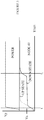
- FIG 3 illustrates the potential on the power rail and on node 49 shown in Figure 2A as a function of time when the ferroelectric capacitor is initially polarized in either the up or down state.
- ferroelectric capacitor 41 If ferroelectric capacitor 41 is in the down state when ferroelectric autonomous memory circuit 40 is powered up, the potential on node 49 initially increases with the power rail potential until the potential at node 49 reaches a value that causes ferroelectric capacitor 41 to begin to change polarization state.
- ferroelectric autonomous memory circuit 40 is powered up with ferroelectric capacitor 41 in the down state, ferroelectric capacitor 41 begins to flip polarization, and charge is released that causes NPN transistor 46 to begin to conduct.
- NPN transistor 46 begins to conduct too much, the potential on node 49 begins to drop and ferroelectric capacitor 41 slows its switching. If NPN transistor 46 does not conduct enough, the potential on node 49 rises faster causing ferroelectric capacitor 41 to switch faster forcing more current into the control input of NPN transistor 46 increasing its conductivity. Thus, the circuit stabilizes with the potential of node 49 at a specific intermediate value with a slow rate of rise. In this manner, the change in conductivity of NPN transistor 46 limits the voltage rise at node 49 until the change in state of ferroelectric capacitor 41 is completed. At this point, no further switching charge will be released from ferroelectric capacitor 41, and hence, NPN transistor 46 will again become non-conducting.
- V s The potential during the transition of ferroelectric capacitor 41 will be referred to as the "shelf voltage", V s , in the following discussion.
- the specific shape of the potential at node 49, or the analogous node in autonomous memory circuits based on other forms of switches, will, in general, depend on the specific switch implementation, and the relationships between the switch, the ferroelectric capacitor, and the sensing element if there is one.
- the potential on the power rail and on node 49 shown in Figure 3 is shown as a function of time when ferroelectric autonomous memory circuit 40 is powered up with ferroelectric capacitor 41 in the up state. Since ferroelectric capacitor 41 does not switch during power up, little current flows into the control input of NPN transistor 46 and NPN transistor 46 never conducts. The potential on node 49 immediately rises to the voltage on the power line 45.
- FIG. 4 illustrates the potential on node 49 when power line 45 is repeatedly pulsed. It is assumed that ferroelectric capacitor 41 is fully polarized in the down state at the beginning of the process. To simplify the following discussion, it will be assumed that the pulses on power line 45 are all of equal duration and amplitude although the circuit may be operated with pulses of dissimilar amplitude and pulse width for purposes other than linear counting. Denote the duration of each pulse at a potential above the shelf voltage by DT. Initially, ferroelectric capacitor 41 is polarized in the down state, and hence, the potential at node 49 rises to V s in response to each pulse on power line 45. Exemplary early pulses are labeled at 51 and 52.
- the corresponding pulses at node 49 are shown at 61 and 62, respectively.
- ferroelectric capacitor 41 When the sum of the DTs is equal to t 2 -t 1 shown in Figure 3 , ferroelectric capacitor 41 will have completely flipped polarization state. Hence, the next pulse will result in the potential at node 49 rising to V p as shown at 63.
- Successive pulses on power line 45 will likewise generate pulses on node 49 that have an amplitude of V p rather than V s .
- the number of pulses needed to flip the polarization such that the response to the next pulse provides a response at V p instead of V s will be referred to as the saturation pulse count in the following discussion.
- the saturation pulse count can be detected by monitoring the voltage on node 49, the saturation pulse count being indicated by a voltage above a threshold value that will be referred to as the count complete threshold.
- ferroelectric capacitor 41 is initially polarized in the down direction by a reset pulse on the RESET line and then subjected to an unknown number of pulses from pulse source 75, the number being less than the saturation count.
- the actual number of counts stored can be determined by connecting power line 45 to V p and measuring the time needed for node 49 to rise to V p as measured by detector 76. This time is related to the saturation pulse count minus the number of pulses that have already been received.
- the current count can be determined by pulsing power line 45 and counting the number of pulses that result in node 49 responding with a voltage substantially above the shelf voltage. The difference between this count and the saturation count can be used to determine the count that was stored in the counter.
- Ferroelectric autonomous memory 40 can be preprogrammed such that a predetermined number of pulses will result in an output signal to detector 76 that is greater than V s .
- ferroelectric capacitor 41 is polarized in the down direction by a reset pulse and then a number of pulses are added to ferroelectric autonomous memory 40. In this case, the number that is initially added is the saturation pulse count less the predetermined number in question.
- detector 76 In a mode in which detector 76 is used to detect the acquisition of the saturation pulse count during actual counting, detector 76 would need to have a power source. During the time in which the count signal is active, detector 76 can be powered from the count pulse source. As will be explained in more detail below, part of the power from the pulse source can be stored to power the counter for a short period of time after the count has been updated. In this case, the detector can return a signal indicating that the saturation count was reached after the pulse has terminated.
- Figure 5A is a schematic drawing of detector 50
- Figure 5B is a symbolic representation of a detector such as detector 50.
- the symbolic representation of a detector is not limited to the specific circuit shown in Figure 5A .
- detector 50 is powered directly from the count signal.
- detector 50 can be powered from any source that is available when the count signal is generated.
- Multi-stage counter 80 counts pulses from a pulse source 90. It is assumed that pulse source 90 has sufficient power to power multi-stage counter 80 during the period in which the pulse signal from pulse source 90 is present. If the time needed to complete the counting operation is greater than the duration of the pulse signal, a power storage device 83 can be utilized to extend the pulse signal.
- power storage device 83 could include a capacitor that stores sufficient power to provide power to the various components during the counting operation.
- stage 81 The least significant "digit" is counted in stage 81.
- an overflow signal is sent to stage 82, which counts the overflow signals from stage 81.
- the overflow signal is used to reset autonomous memory circuit 86 in stage 81 after a delay that is generated by delay circuit 87.
- Delay circuit 87 must provide a sufficient delay to prevent a race condition from causing autonomous memory circuit 86 to reset before the output of stage 81 triggers a count in stage 82.
- the power connections to the delay circuits have been omitted from the drawing. In general, the delay circuit only needs to be active during the time needed to complete the stage updates associated with the current count. Hence, if power is needed, the power can be supplied by power storage device 83.
- a pulse shaping circuit such as one shot 88 can be included in the stages.
- the one shots ensure that each pulse that is counted has the same shape and hence, each pulse contributes the same amount of charge to the ferroelectric capacitor.
- the one shots trigger off of the raising edge of the input signal to the one shots, the time needed to complete the counting operation can be reduced.
- the minimum length pulse needed to count is significantly less than the duration of the pulse from the pulse source.
- the power storage mechanism must provide power for a period of time that is long enough for the count completion signals to propagate through all of the stages of the counter. By shortening the pulse length for the pulse that is actually counted, the amount of time that power storage device 83 must maintain power can be significantly reduced.
- a multi-stage counter can also, in principle, be read out by adding pulses until the last stage generates a count completed signal. The number of pulses that must be added and the known capacity of the counter can then be used to determine the count that was actually in the counter at the start of the readout process. However, for counters with a large number of stages, the readout time can be excessive.
- each stage of the counter is readout in parallel by isolating that stage from the stages on each side of that stage and routing the count complete signals from each stage to a controller. The isolated stages are then pulsed in parallel and the number of pulses needed to cause a count complete signal to be generated in that stage is determined.
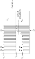
- Multi-stage counter 100 includes a switch 103 that is open during normal counting. This switch limits the pulse input to the one shot in the least significant count stage. During readout, switch 103 is closed. As a result, the pulses from pulse generator 111 are routed to the one shot in each of the stages.
- Each of the stages with the exception of the last stage includes an isolation switch such as isolation switch 104. The isolation switch blocks the count complete signal from the stage in question from being input to the next stage. Isolation switch 104 is also opened during the readout operation.
- Multi-stage counter 100 also routes the count complete signals to externally available conductors.
- the external conductors for stages 101 and 102 are shown at 101a and 102a, respectively.
- the count in multi-stage counter 100 is determined with the aid of a controller 110 that includes a pulse generator 111 that provides the readout pulses to the stages and a power source 112.
- power source 112 is optional, in that the power storage component could also power multi-stage counter 100 during readout.
- Controller 110 monitors the count complete signal lines from each stage and records the number of pulses that resulted in the count complete signal being generated by each stage.
- a counter stage can be readout by applying a long DC signal to the count input of that stage and measuring the time between the start of that signal and the time at which the count complete signal from that stage is observed.
- Figure 8 illustrates a system in which the counter is readout by measuring the time that it takes for each stage to generate a count complete signal after a long readout pulse is applied to the count input of that stage.
- Counter 200 includes a number of elements that are analogous to elements discussed above with respect to multi-stage counter 100.
- Counter 200 has a plurality of count stages such as stages 201 and 202. Counter 200 differs from counter 100 in that a separate readout port 221 couples the count input of each autonomous memory cell to an external readout controller 210.
- a signal generator 211 generates a continuous readout pulse that is applied to readout port 221.
- Each count stage of counter 200 is isolated from the other stages by switches such as isolation switch 104.
- External readout controller 210 has access to the count complete signals generated in each count stage via ports 101a, 102a, ... The controller measures the times from the start of the readout pulse to the time at which a count complete signal is detected on each of these ports.
- the maximum count that can be stored in a single stage counter depends on the ratio of the charge transferred to the ferroelectric capacitor during each pulse to the total charge needed to flip the polarization of the ferroelectric capacitor. Assume that the ferroelectric capacitor starts in a configuration that is fully polarized down. Each positive pulse on the count line moves the polarization toward the state in which the ferroelectric capacitor is fully polarized in the up direction. When the ferroelectric capacitor reaches the fully polarized state, the counter is saturated and the voltage at node 49 rises to the voltage of the pulse.
- the ratio of the charge needed to flip the polarization of the capacitor to the charge transferred by a pulse must be maximized.
- using a large resistor as the conductive load results in a small charge being transferred to the ferroelectric capacitor.
- the minimum size of the pulse charge that is set by noise.
- a small conductive load results in a larger charge being transferred to node 49 unless a portion of the charge is shunted around the ferroelectric capacitor.
- the size of the ferroelectric capacitor must be increased and/or the part of the charge that is shunted around the ferroelectric capacitor by transistor 46 must be increased.
- the fraction of the charge that is shunted around the ferroelectric capacitor depends on the beta of transistor 46.
- the maximum count can also be increased by increasing the beta of transistor 46.
- the shelf voltage on which the present invention depends is a function of the ferroelectric capacitor and the conductive load. If the switch were removed leaving a ferroelectric capacitor in series with the conductive load, a shelf voltage effect similar to that described above would be observed if the ferroelectric capacitor started in one polarized state and the pulse moved the ferroelectric capacitor toward the other polarized state. However, a large conductive load would be needed as all of the charge generated by the pulse enters the ferroelectric capacitor. As noted above, the switch provides a mechanism for shunting part of the current around the ferroelectric capacitor.
- the switch allows the ferroelectric capacitor to reset to the down state again by inputting a pulse having the same polarity as the count pulse into the control input of the switch while keeping the count line connected to ground.
- the arrangement shown in Figure 2A is particularly advantageous in that a single transistor provides both of these functions.
Landscapes
- Engineering & Computer Science (AREA)
- Power Engineering (AREA)
- Computer Hardware Design (AREA)
- Static Random-Access Memory (AREA)
- Measurement Of Unknown Time Intervals (AREA)
Claims (12)
- Vorrichtung, umfassend:
eine erste Zählstufe (81, 101), umfassend:einen ferroelektrischen Kondensator (21, 42) mit ersten und zweiten Polarisationszuständen;ein variables Impedanzelement (23) mit einer Impedanz zwischen ersten und zweiten Schalterklemmen, die durch ein Signal auf einer Steuerklemme bestimmt wird, wobei der ferroelektrische Kondensator zwischen der Steuerklemme und der ersten Schalterklemme verbunden ist;einen Reset-Port, der konfiguriert ist, ein Reset-Signal mit der Steuerklemme zu verbinden, wobei das Reset-Signal bewirkt, dass der ferroelektrische Kondensator in den ersten Polarisationszustand polarisiert wird;einen Zähl-Port, der konfiguriert ist, zu zählende Impulse zu empfangen, wobei der Zähl-Port über eine leitfähige Last mit der ersten Schalterklemme verbunden ist; undeinen Detektor (76), der ein Zählabschlusssignal generiert, falls ein Potenzial an der ersten Schalterklemme einen Schwellenwert überschreitet, während der Zähl-Port einen der Impulse empfängt, dadurch gekennzeichnet, dass:
die erste Zählstufe eine Verzögerungsschaltung umfasst, die das Zählabschlusssignal der Zählung der ersten Zählstufe mit dem Reset-Port der ersten Zählstufe nach einer vorbestimmten Zeitverzögerung koppelt, und wobei die Vorrichtung ferner eine zweite Zählstufe (82, 102) umfasst, wobei die zweite Zählstufe umfasst:einen ferroelektrischen Kondensator (21, 41) mit ersten und zweiten Polarisationszuständen;ein variables Impedanzelement (23) mit einer Impedanz zwischen dritten und vierten Schalterklemmen, die durch ein Signal auf einer weiteren Steuerklemme bestimmt wird, wobei der ferroelektrische Kondensator der zweiten Zählstufe zwischen der weiteren Steuerklemme und der dritten Schalterklemme verbunden ist;einen Reset-Port, der konfiguriert ist, ein Reset-Signal mit der weiteren Steuerklemme zu verbinden, wobei das Reset-Signal bewirkt, dass der ferroelektrische Kondensator der zweiten Zählstufe in den ersten Polarisationszustand polarisiert wird;einen Zähl-Port, der konfiguriert ist, zu zählende Impulse zu empfangen, wobei der Zähl-Port über eine weitere leitfähige Last mit der dritten Schalterklemme verbunden ist;einen Detektor (76), der Zählabschlusssignal generiert, falls ein Potenzial an der dritten Schalterklemme einen Schwellenwert überschreitet, während der Zähl-Port der zweiten Zählstufe einen der Impulse empfängt, wobeidas Zählabschlusssignal der ersten Zählstufe mit dem Zähl-Port der zweiten Zählstufe gekoppelt ist. - Vorrichtung nach Anspruch 1, wobei der Zähl-Port der ersten Zählstufe eine Schaltung umfasst, die einen vorbestimmten Impuls aus jedem der empfangenen Impulse generiert, wobei der vorbestimmte Impuls mit der leitfähigen Last gekoppelt wird.
- Verfahren zum Zählen von Impulsen, wobei das Verfahren umfasst:Bereitstellen einer ersten Zählstufe (81, 101), umfassend:einen ferroelektrischen Kondensator (21, 41) mit ersten und zweiten Polarisationszuständen; undein variables Impedanzelement (23) mit einer Impedanz zwischen ersten und zweiten Schalterklemmen, die durch ein Signal auf einer Steuerklemme bestimmt wird, wobei der ferroelektrische Kondensator zwischen der Steuerklemme und der ersten Schalterklemme verbunden ist;Bewirken, dass der ferroelektrische Kondensator im ersten Polarisationszustand polarisiert wird;Anwenden einer Vielzahl zu zählender Impulse auf die erste Schalterklemme durch eine leitfähige Last; undGenerieren eines Zählabschlusssignals, falls ein Potenzial auf der ersten Schalterklemme einen Schwellenwert überschreitet, wenn eine Vielzahl von Impulsen angewandt wird, gekennzeichnet durch:Bereitstellen einer zweiten Zählstufe (82, 102), umfassend:einen ferroelektrischen Kondensator (21, 41) mit ersten und zweiten Polarisationszuständen; undein variables Impedanzelement (23) mit einer Impedanz zwischen dritten und vierten Schalterklemmen, die durch ein Signal auf einer weiteren Steuerklemme bestimmt wird, wobei der ferroelektrische Kondensator der zweiten Zählstufe zwischen der weiteren Steuerklemme und der dritten Schalterklemme verbunden ist;Bewirken, dass der ferroelektrische Kondensator der zweiten Zählstufe im ersten Polarisationszustand polarisiert wird; undAnwenden eines vom Zählabschlusssignal abgeleiteten Signals, das von der ersten Zählstufe generiert wurde, auf die dritte Schalterklemme der zweiten Zählstufe über eine weitere leitfähige Last.
- Verfahren nach Anspruch 3 oder die Vorrichtung nach Anspruch 1, wobei das Zählabschlusssignal von einer Schaltung generiert wird, die alleinig von der Vielzahl von Impulsen angetrieben wird.
- Verfahren nach Anspruch 3, wobei jeder der Vielzahl von Impulsen durch eine Impulsdauer und eine Impulsamplitude gekennzeichnet ist, und wobei die Impulsdauer und die Impulsamplitude jedes der Vielzahl von Impulsen identisch sind.
- Verfahren nach Anspruch 3, welches bewirkt, dass der ferroelektrische Kondensator der ersten Zählstufe im ersten Polarisationszustand nach einer Verzögerung polarisiert wird, wenn das Zählabschlusssignal generiert ist.
- Verfahren nach Anspruch 3, das ferner das Ermitteln einer Zahl von Impulsen umfasst, die auf die erste Schalterklemme angewandt worden ist, seit bewirkt wurde, dass sich der ferroelektrische Kondensator der ersten Zählstufe im ersten Polarisationszustand befindet, nämlich durch Ermitteln einer Zahl zusätzlicher Impulse, die auf die erste Schalterklemme angewandt werden müssen, um zu bewirken, dass die erste Schalterklemme den Schwellenwert überschreitet.
- Verfahren nach Anspruch 3 ferner umfassend:Isolieren der ersten Zählstufe von der zweiten Zählstufe; undErmitteln einer Zahl von Impulsen, die auf die ersten und dritten Schalterklemmen angewandt worden sind, durch unabhängiges Ermitteln der Zahl von zusätzlichen Impulsen, die auf die ersten und dritten Schalterklemmen angewandt werden müssen, um zu bewirken, dass die ersten und dritten Schalterklemmen den Schwellenwert überschreiten.
- System, umfassend:
die Vorrichtung nach Anspruch 1 und eine Ausleseschaltung, wobei die Ausleseschaltung umfasst:einen Auslesegenerator, der ein Auslesesignal mit einem Zähl-Port der ersten Zählstufe koppelt; undein Steuergerät, das die Zahl der Impulse ermittelt, die erforderlich sind, um zu bewirken, dass der Detektor der ersten Zählstufe das Zählabschlusssignal generiert. - System nach Anspruch 9, wobei das Auslesesignal eine Reihe von Ausleseimpulsen umfasst.
- System nach Anspruch 9, wobei das Auslesesignal ein Gleichstromsignal (DC-Signal) umfasst, das zu einer ersten Zeit angewandt wird und das Steuergerät misst eine Zeit, zu der das Zählabschlusssignal relativ zur ersten Zeit generiert wird.
- System nach Anspruch 9, wobei die Ausleseschaltung eine von der ersten Zählstufe separate, abnehmbare Komponente ist.
Applications Claiming Priority (2)
| Application Number | Priority Date | Filing Date | Title |
|---|---|---|---|
| US14/160,343 US9269416B2 (en) | 2010-11-30 | 2014-01-21 | Non-volatile counter utilizing a ferroelectric capacitor |
| PCT/US2015/012260 WO2015112609A1 (en) | 2014-01-21 | 2015-01-21 | Non-volatile counter utilizing a ferroelectric capacitor |
Publications (3)
| Publication Number | Publication Date |
|---|---|
| EP3097643A1 EP3097643A1 (de) | 2016-11-30 |
| EP3097643A4 EP3097643A4 (de) | 2017-01-25 |
| EP3097643B1 true EP3097643B1 (de) | 2018-11-21 |
Family
ID=53681903
Family Applications (1)
| Application Number | Title | Priority Date | Filing Date |
|---|---|---|---|
| EP15740718.0A Not-in-force EP3097643B1 (de) | 2014-01-21 | 2015-01-21 | Nichtflüchtiger zähler mit einem ferroelektrischen kondensator |
Country Status (5)
| Country | Link |
|---|---|
| EP (1) | EP3097643B1 (de) |
| JP (1) | JP6524540B2 (de) |
| KR (1) | KR102287033B1 (de) |
| CN (1) | CN106105037B (de) |
| WO (1) | WO2015112609A1 (de) |
Families Citing this family (1)
| Publication number | Priority date | Publication date | Assignee | Title |
|---|---|---|---|---|
| JP7702411B2 (ja) | 2020-08-03 | 2025-07-03 | 株式会社半導体エネルギー研究所 | 半導体装置の駆動方法 |
Family Cites Families (13)
| Publication number | Priority date | Publication date | Assignee | Title |
|---|---|---|---|---|
| JP2561750B2 (ja) * | 1990-10-30 | 1996-12-11 | 三菱電機株式会社 | パルス発生回路 |
| US5539279A (en) * | 1993-06-23 | 1996-07-23 | Hitachi, Ltd. | Ferroelectric memory |
| WO2004010582A1 (ja) * | 2002-07-22 | 2004-01-29 | Matsushita Electric Industrial Co., Ltd. | 確率的演算素子、その駆動方法及びこれを用いた認識処理装置 |
| JP2004304381A (ja) * | 2003-03-31 | 2004-10-28 | Matsushita Electric Ind Co Ltd | カウンタ装置およびカウント方法 |
| JP4157553B2 (ja) * | 2003-05-27 | 2008-10-01 | 富士通株式会社 | 強誘電体メモリ |
| JP2005044412A (ja) * | 2003-07-24 | 2005-02-17 | Seiko Epson Corp | 不揮発性記憶装置およびこれを用いた電子機器。 |
| US7116572B2 (en) * | 2004-11-09 | 2006-10-03 | Ramtron International Corporation | Circuit for generating a centered reference voltage for a 1T/1C ferroelectric memory |
| US7990749B2 (en) * | 2009-06-08 | 2011-08-02 | Radiant Technology, Inc. | Variable impedance circuit controlled by a ferroelectric capacitor |
| CN101777139B (zh) * | 2009-12-30 | 2013-07-17 | 宁波大学 | 一种基于神经mos管的多值计数器单元及多位多值计数器 |
| US8824186B2 (en) * | 2010-06-09 | 2014-09-02 | Radiant Technologies, Inc. | Embedded non-volatile memory circuit for implementing logic functions across periods of power disruption |
| CN103026414B (zh) * | 2010-06-11 | 2016-02-03 | 拉迪安特技术公司 | 由铁电电容器控制的可变阻抗电路 |
| KR101153813B1 (ko) * | 2010-09-30 | 2012-06-13 | 에스케이하이닉스 주식회사 | 반도체 메모리 장치 |
| US8760907B2 (en) * | 2010-11-30 | 2014-06-24 | Radiant Technologies, Inc. | Analog memories utilizing ferroelectric capacitors |
-
2015
- 2015-01-21 CN CN201580012228.5A patent/CN106105037B/zh active Active
- 2015-01-21 WO PCT/US2015/012260 patent/WO2015112609A1/en not_active Ceased
- 2015-01-21 JP JP2016546914A patent/JP6524540B2/ja not_active Expired - Fee Related
- 2015-01-21 KR KR1020167022256A patent/KR102287033B1/ko not_active Expired - Fee Related
- 2015-01-21 EP EP15740718.0A patent/EP3097643B1/de not_active Not-in-force
Non-Patent Citations (1)
| Title |
|---|
| None * |
Also Published As
| Publication number | Publication date |
|---|---|
| CN106105037A (zh) | 2016-11-09 |
| JP6524540B2 (ja) | 2019-06-05 |
| KR102287033B1 (ko) | 2021-08-09 |
| EP3097643A1 (de) | 2016-11-30 |
| CN106105037B (zh) | 2019-03-29 |
| WO2015112609A1 (en) | 2015-07-30 |
| KR20160110464A (ko) | 2016-09-21 |
| EP3097643A4 (de) | 2017-01-25 |
| JP2017508358A (ja) | 2017-03-23 |
Similar Documents
| Publication | Publication Date | Title |
|---|---|---|
| US9269416B2 (en) | Non-volatile counter utilizing a ferroelectric capacitor | |
| US7990749B2 (en) | Variable impedance circuit controlled by a ferroelectric capacitor | |
| US3428828A (en) | Sample and hold circuit | |
| JP2017529046A5 (de) | ||
| JP2017511112A (ja) | 電気エネルギー貯蔵システム | |
| EP4401276A2 (de) | Vorladen und verbinden eines energiespeichersystems | |
| EP2580757B1 (de) | Anhand eines ferroelektrischen kondensators gesteuerter schaltkreis mit variabler impedanz | |
| EP3097643B1 (de) | Nichtflüchtiger zähler mit einem ferroelektrischen kondensator | |
| CN108400781B (zh) | 功率开关装置及其操作方法 | |
| US8565000B2 (en) | Variable impedance circuit controlled by a ferroelectric capacitor | |
| JP2011507477A (ja) | Dc−dcコンバータを有する集積回路 | |
| US3189751A (en) | Timing circuit | |
| US3441810A (en) | Multiple-mode solid-state time delay apparatus including charge-monitoring timing circuits | |
| CN108462484A (zh) | 自泵压过流保护型n管输出高边驱动电路 | |
| US5710690A (en) | Method and apparatus for protecting an integrated circuit from current overload | |
| US3371222A (en) | Bi-directional ring counter | |
| JP2022028348A5 (de) | ||
| US3758872A (en) | Fast recovery circuit for ac amplifier | |
| EP3646039A1 (de) | Kondensator und diagnostische prüfung eines kapazitiven sensors | |
| CN208272942U (zh) | 自泵压过流保护型n管输出高边驱动电路 | |
| KR102175055B1 (ko) | 두 전극에 각각 형성된 커패시턴스의 차이를 측정하는 방법 및 이를 이용한 터치입력 검출방법 | |
| SU445084A1 (ru) | Устройство дл управлени пол ризованным реле | |
| EP2870604B1 (de) | Eingebettete nichtflüchtige speicherschaltung zur durchführung logischer funktionen in stromunterbrechungsphasen | |
| US3413489A (en) | Frequency divider arrangement | |
| US20130135013A1 (en) | Multi-stage Sample and Hold Circuit |
Legal Events
| Date | Code | Title | Description |
|---|---|---|---|
| PUAI | Public reference made under article 153(3) epc to a published international application that has entered the european phase |
Free format text: ORIGINAL CODE: 0009012 |
|
| 17P | Request for examination filed |
Effective date: 20160803 |
|
| AK | Designated contracting states |
Kind code of ref document: A1 Designated state(s): AL AT BE BG CH CY CZ DE DK EE ES FI FR GB GR HR HU IE IS IT LI LT LU LV MC MK MT NL NO PL PT RO RS SE SI SK SM TR |
|
| AX | Request for extension of the european patent |
Extension state: BA ME |
|
| A4 | Supplementary search report drawn up and despatched |
Effective date: 20161223 |
|
| RIC1 | Information provided on ipc code assigned before grant |
Ipc: H03K 23/76 20060101ALI20161219BHEP Ipc: H03K 21/08 20060101AFI20161219BHEP Ipc: G11C 11/22 20060101ALN20161219BHEP |
|
| DAX | Request for extension of the european patent (deleted) | ||
| RIC1 | Information provided on ipc code assigned before grant |
Ipc: H03K 23/76 20060101ALI20180406BHEP Ipc: H03K 21/08 20060101AFI20180406BHEP Ipc: G11C 11/22 20060101ALN20180406BHEP |
|
| GRAP | Despatch of communication of intention to grant a patent |
Free format text: ORIGINAL CODE: EPIDOSNIGR1 |
|
| STAA | Information on the status of an ep patent application or granted ep patent |
Free format text: STATUS: GRANT OF PATENT IS INTENDED |
|
| INTG | Intention to grant announced |
Effective date: 20180608 |
|
| GRAS | Grant fee paid |
Free format text: ORIGINAL CODE: EPIDOSNIGR3 |
|
| GRAA | (expected) grant |
Free format text: ORIGINAL CODE: 0009210 |
|
| STAA | Information on the status of an ep patent application or granted ep patent |
Free format text: STATUS: THE PATENT HAS BEEN GRANTED |
|
| AK | Designated contracting states |
Kind code of ref document: B1 Designated state(s): AL AT BE BG CH CY CZ DE DK EE ES FI FR GB GR HR HU IE IS IT LI LT LU LV MC MK MT NL NO PL PT RO RS SE SI SK SM TR |
|
| REG | Reference to a national code |
Ref country code: CH Ref legal event code: EP |
|
| REG | Reference to a national code |
Ref country code: IE Ref legal event code: FG4D |
|
| REG | Reference to a national code |
Ref country code: DE Ref legal event code: R096 Ref document number: 602015020022 Country of ref document: DE |
|
| REG | Reference to a national code |
Ref country code: AT Ref legal event code: REF Ref document number: 1068744 Country of ref document: AT Kind code of ref document: T Effective date: 20181215 |
|
| REG | Reference to a national code |
Ref country code: NL Ref legal event code: MP Effective date: 20181121 |
|
| REG | Reference to a national code |
Ref country code: AT Ref legal event code: MK05 Ref document number: 1068744 Country of ref document: AT Kind code of ref document: T Effective date: 20181121 |
|
| PG25 | Lapsed in a contracting state [announced via postgrant information from national office to epo] |
Ref country code: LV Free format text: LAPSE BECAUSE OF FAILURE TO SUBMIT A TRANSLATION OF THE DESCRIPTION OR TO PAY THE FEE WITHIN THE PRESCRIBED TIME-LIMIT Effective date: 20181121 Ref country code: AT Free format text: LAPSE BECAUSE OF FAILURE TO SUBMIT A TRANSLATION OF THE DESCRIPTION OR TO PAY THE FEE WITHIN THE PRESCRIBED TIME-LIMIT Effective date: 20181121 Ref country code: FI Free format text: LAPSE BECAUSE OF FAILURE TO SUBMIT A TRANSLATION OF THE DESCRIPTION OR TO PAY THE FEE WITHIN THE PRESCRIBED TIME-LIMIT Effective date: 20181121 Ref country code: IS Free format text: LAPSE BECAUSE OF FAILURE TO SUBMIT A TRANSLATION OF THE DESCRIPTION OR TO PAY THE FEE WITHIN THE PRESCRIBED TIME-LIMIT Effective date: 20190321 Ref country code: BG Free format text: LAPSE BECAUSE OF FAILURE TO SUBMIT A TRANSLATION OF THE DESCRIPTION OR TO PAY THE FEE WITHIN THE PRESCRIBED TIME-LIMIT Effective date: 20190221 Ref country code: NO Free format text: LAPSE BECAUSE OF FAILURE TO SUBMIT A TRANSLATION OF THE DESCRIPTION OR TO PAY THE FEE WITHIN THE PRESCRIBED TIME-LIMIT Effective date: 20190221 Ref country code: HR Free format text: LAPSE BECAUSE OF FAILURE TO SUBMIT A TRANSLATION OF THE DESCRIPTION OR TO PAY THE FEE WITHIN THE PRESCRIBED TIME-LIMIT Effective date: 20181121 Ref country code: ES Free format text: LAPSE BECAUSE OF FAILURE TO SUBMIT A TRANSLATION OF THE DESCRIPTION OR TO PAY THE FEE WITHIN THE PRESCRIBED TIME-LIMIT Effective date: 20181121 Ref country code: LT Free format text: LAPSE BECAUSE OF FAILURE TO SUBMIT A TRANSLATION OF THE DESCRIPTION OR TO PAY THE FEE WITHIN THE PRESCRIBED TIME-LIMIT Effective date: 20181121 |
|
| PG25 | Lapsed in a contracting state [announced via postgrant information from national office to epo] |
Ref country code: GR Free format text: LAPSE BECAUSE OF FAILURE TO SUBMIT A TRANSLATION OF THE DESCRIPTION OR TO PAY THE FEE WITHIN THE PRESCRIBED TIME-LIMIT Effective date: 20190222 Ref country code: NL Free format text: LAPSE BECAUSE OF FAILURE TO SUBMIT A TRANSLATION OF THE DESCRIPTION OR TO PAY THE FEE WITHIN THE PRESCRIBED TIME-LIMIT Effective date: 20181121 Ref country code: PT Free format text: LAPSE BECAUSE OF FAILURE TO SUBMIT A TRANSLATION OF THE DESCRIPTION OR TO PAY THE FEE WITHIN THE PRESCRIBED TIME-LIMIT Effective date: 20190321 Ref country code: AL Free format text: LAPSE BECAUSE OF FAILURE TO SUBMIT A TRANSLATION OF THE DESCRIPTION OR TO PAY THE FEE WITHIN THE PRESCRIBED TIME-LIMIT Effective date: 20181121 Ref country code: SE Free format text: LAPSE BECAUSE OF FAILURE TO SUBMIT A TRANSLATION OF THE DESCRIPTION OR TO PAY THE FEE WITHIN THE PRESCRIBED TIME-LIMIT Effective date: 20181121 Ref country code: RS Free format text: LAPSE BECAUSE OF FAILURE TO SUBMIT A TRANSLATION OF THE DESCRIPTION OR TO PAY THE FEE WITHIN THE PRESCRIBED TIME-LIMIT Effective date: 20181121 |
|
| PG25 | Lapsed in a contracting state [announced via postgrant information from national office to epo] |
Ref country code: PL Free format text: LAPSE BECAUSE OF FAILURE TO SUBMIT A TRANSLATION OF THE DESCRIPTION OR TO PAY THE FEE WITHIN THE PRESCRIBED TIME-LIMIT Effective date: 20181121 Ref country code: IT Free format text: LAPSE BECAUSE OF FAILURE TO SUBMIT A TRANSLATION OF THE DESCRIPTION OR TO PAY THE FEE WITHIN THE PRESCRIBED TIME-LIMIT Effective date: 20181121 Ref country code: CZ Free format text: LAPSE BECAUSE OF FAILURE TO SUBMIT A TRANSLATION OF THE DESCRIPTION OR TO PAY THE FEE WITHIN THE PRESCRIBED TIME-LIMIT Effective date: 20181121 Ref country code: DK Free format text: LAPSE BECAUSE OF FAILURE TO SUBMIT A TRANSLATION OF THE DESCRIPTION OR TO PAY THE FEE WITHIN THE PRESCRIBED TIME-LIMIT Effective date: 20181121 |
|
| REG | Reference to a national code |
Ref country code: DE Ref legal event code: R097 Ref document number: 602015020022 Country of ref document: DE |
|
| PG25 | Lapsed in a contracting state [announced via postgrant information from national office to epo] |
Ref country code: RO Free format text: LAPSE BECAUSE OF FAILURE TO SUBMIT A TRANSLATION OF THE DESCRIPTION OR TO PAY THE FEE WITHIN THE PRESCRIBED TIME-LIMIT Effective date: 20181121 Ref country code: SK Free format text: LAPSE BECAUSE OF FAILURE TO SUBMIT A TRANSLATION OF THE DESCRIPTION OR TO PAY THE FEE WITHIN THE PRESCRIBED TIME-LIMIT Effective date: 20181121 Ref country code: SM Free format text: LAPSE BECAUSE OF FAILURE TO SUBMIT A TRANSLATION OF THE DESCRIPTION OR TO PAY THE FEE WITHIN THE PRESCRIBED TIME-LIMIT Effective date: 20181121 Ref country code: EE Free format text: LAPSE BECAUSE OF FAILURE TO SUBMIT A TRANSLATION OF THE DESCRIPTION OR TO PAY THE FEE WITHIN THE PRESCRIBED TIME-LIMIT Effective date: 20181121 Ref country code: MC Free format text: LAPSE BECAUSE OF FAILURE TO SUBMIT A TRANSLATION OF THE DESCRIPTION OR TO PAY THE FEE WITHIN THE PRESCRIBED TIME-LIMIT Effective date: 20181121 |
|
| REG | Reference to a national code |
Ref country code: CH Ref legal event code: PL |
|
| PLBE | No opposition filed within time limit |
Free format text: ORIGINAL CODE: 0009261 |
|
| STAA | Information on the status of an ep patent application or granted ep patent |
Free format text: STATUS: NO OPPOSITION FILED WITHIN TIME LIMIT |
|
| PG25 | Lapsed in a contracting state [announced via postgrant information from national office to epo] |
Ref country code: LU Free format text: LAPSE BECAUSE OF NON-PAYMENT OF DUE FEES Effective date: 20190121 |
|
| REG | Reference to a national code |
Ref country code: BE Ref legal event code: MM Effective date: 20190131 |
|
| GBPC | Gb: european patent ceased through non-payment of renewal fee |
Effective date: 20190221 |
|
| 26N | No opposition filed |
Effective date: 20190822 |
|
| REG | Reference to a national code |
Ref country code: IE Ref legal event code: MM4A |
|
| PG25 | Lapsed in a contracting state [announced via postgrant information from national office to epo] |
Ref country code: SI Free format text: LAPSE BECAUSE OF FAILURE TO SUBMIT A TRANSLATION OF THE DESCRIPTION OR TO PAY THE FEE WITHIN THE PRESCRIBED TIME-LIMIT Effective date: 20181121 |
|
| PG25 | Lapsed in a contracting state [announced via postgrant information from national office to epo] |
Ref country code: BE Free format text: LAPSE BECAUSE OF NON-PAYMENT OF DUE FEES Effective date: 20190131 |
|
| PG25 | Lapsed in a contracting state [announced via postgrant information from national office to epo] |
Ref country code: CH Free format text: LAPSE BECAUSE OF NON-PAYMENT OF DUE FEES Effective date: 20190131 Ref country code: LI Free format text: LAPSE BECAUSE OF NON-PAYMENT OF DUE FEES Effective date: 20190131 |
|
| PG25 | Lapsed in a contracting state [announced via postgrant information from national office to epo] |
Ref country code: IE Free format text: LAPSE BECAUSE OF NON-PAYMENT OF DUE FEES Effective date: 20190121 Ref country code: GB Free format text: LAPSE BECAUSE OF NON-PAYMENT OF DUE FEES Effective date: 20190221 |
|
| PG25 | Lapsed in a contracting state [announced via postgrant information from national office to epo] |
Ref country code: TR Free format text: LAPSE BECAUSE OF FAILURE TO SUBMIT A TRANSLATION OF THE DESCRIPTION OR TO PAY THE FEE WITHIN THE PRESCRIBED TIME-LIMIT Effective date: 20181121 |
|
| PG25 | Lapsed in a contracting state [announced via postgrant information from national office to epo] |
Ref country code: MT Free format text: LAPSE BECAUSE OF NON-PAYMENT OF DUE FEES Effective date: 20190121 |
|
| PG25 | Lapsed in a contracting state [announced via postgrant information from national office to epo] |
Ref country code: CY Free format text: LAPSE BECAUSE OF FAILURE TO SUBMIT A TRANSLATION OF THE DESCRIPTION OR TO PAY THE FEE WITHIN THE PRESCRIBED TIME-LIMIT Effective date: 20181121 |
|
| PG25 | Lapsed in a contracting state [announced via postgrant information from national office to epo] |
Ref country code: HU Free format text: LAPSE BECAUSE OF FAILURE TO SUBMIT A TRANSLATION OF THE DESCRIPTION OR TO PAY THE FEE WITHIN THE PRESCRIBED TIME-LIMIT; INVALID AB INITIO Effective date: 20150121 |
|
| PG25 | Lapsed in a contracting state [announced via postgrant information from national office to epo] |
Ref country code: MK Free format text: LAPSE BECAUSE OF FAILURE TO SUBMIT A TRANSLATION OF THE DESCRIPTION OR TO PAY THE FEE WITHIN THE PRESCRIBED TIME-LIMIT Effective date: 20181121 |
|
| PGFP | Annual fee paid to national office [announced via postgrant information from national office to epo] |
Ref country code: FR Payment date: 20230124 Year of fee payment: 9 |
|
| PGFP | Annual fee paid to national office [announced via postgrant information from national office to epo] |
Ref country code: DE Payment date: 20230123 Year of fee payment: 9 |
|
| REG | Reference to a national code |
Ref country code: DE Ref legal event code: R119 Ref document number: 602015020022 Country of ref document: DE |
|
| PG25 | Lapsed in a contracting state [announced via postgrant information from national office to epo] |
Ref country code: DE Free format text: LAPSE BECAUSE OF NON-PAYMENT OF DUE FEES Effective date: 20240801 |
|
| PG25 | Lapsed in a contracting state [announced via postgrant information from national office to epo] |
Ref country code: FR Free format text: LAPSE BECAUSE OF NON-PAYMENT OF DUE FEES Effective date: 20240131 |
|
| PG25 | Lapsed in a contracting state [announced via postgrant information from national office to epo] |
Ref country code: FR Free format text: LAPSE BECAUSE OF NON-PAYMENT OF DUE FEES Effective date: 20240131 Ref country code: DE Free format text: LAPSE BECAUSE OF NON-PAYMENT OF DUE FEES Effective date: 20240801 |