EP3099493B1 - Barres d'impression et procédés de formation de barres d'impression - Google Patents
Barres d'impression et procédés de formation de barres d'impression Download PDFInfo
- Publication number
- EP3099493B1 EP3099493B1 EP14881051.8A EP14881051A EP3099493B1 EP 3099493 B1 EP3099493 B1 EP 3099493B1 EP 14881051 A EP14881051 A EP 14881051A EP 3099493 B1 EP3099493 B1 EP 3099493B1
- Authority
- EP
- European Patent Office
- Prior art keywords
- pcb
- printhead die
- adhesive material
- recess
- recesses
- Prior art date
- Legal status (The legal status is an assumption and is not a legal conclusion. Google has not performed a legal analysis and makes no representation as to the accuracy of the status listed.)
- Not-in-force
Links
- 238000000034 method Methods 0.000 title claims description 38
- 239000000463 material Substances 0.000 claims description 93
- 239000000853 adhesive Substances 0.000 claims description 81
- 230000001070 adhesive effect Effects 0.000 claims description 81
- 239000012530 fluid Substances 0.000 claims description 35
- 238000007639 printing Methods 0.000 claims description 32
- 238000000465 moulding Methods 0.000 claims description 12
- 238000004891 communication Methods 0.000 claims description 6
- 230000008878 coupling Effects 0.000 claims description 4
- 238000010168 coupling process Methods 0.000 claims description 4
- 238000005859 coupling reaction Methods 0.000 claims description 4
- 239000000758 substrate Substances 0.000 description 19
- 230000008569 process Effects 0.000 description 17
- 239000004593 Epoxy Substances 0.000 description 9
- 230000015572 biosynthetic process Effects 0.000 description 5
- 238000010586 diagram Methods 0.000 description 4
- QHZSDTDMQZPUKC-UHFFFAOYSA-N 3,5-dichlorobiphenyl Chemical compound ClC1=CC(Cl)=CC(C=2C=CC=CC=2)=C1 QHZSDTDMQZPUKC-UHFFFAOYSA-N 0.000 description 3
- 230000005012 migration Effects 0.000 description 3
- 238000013508 migration Methods 0.000 description 3
- 239000004065 semiconductor Substances 0.000 description 3
- XUIMIQQOPSSXEZ-UHFFFAOYSA-N Silicon Chemical compound [Si] XUIMIQQOPSSXEZ-UHFFFAOYSA-N 0.000 description 2
- 239000007788 liquid Substances 0.000 description 2
- 238000004519 manufacturing process Methods 0.000 description 2
- 230000004044 response Effects 0.000 description 2
- 229910052710 silicon Inorganic materials 0.000 description 2
- 239000010703 silicon Substances 0.000 description 2
- 239000007787 solid Substances 0.000 description 2
- 239000010409 thin film Substances 0.000 description 2
- SXZSFWHOSHAKMN-UHFFFAOYSA-N 2,3,4,4',5-Pentachlorobiphenyl Chemical compound C1=CC(Cl)=CC=C1C1=CC(Cl)=C(Cl)C(Cl)=C1Cl SXZSFWHOSHAKMN-UHFFFAOYSA-N 0.000 description 1
- 230000000712 assembly Effects 0.000 description 1
- 238000000429 assembly Methods 0.000 description 1
- 230000005465 channeling Effects 0.000 description 1
- 238000003486 chemical etching Methods 0.000 description 1
- 239000011248 coating agent Substances 0.000 description 1
- 238000000576 coating method Methods 0.000 description 1
- 239000003086 colorant Substances 0.000 description 1
- 230000000052 comparative effect Effects 0.000 description 1
- 150000001875 compounds Chemical class 0.000 description 1
- 239000004020 conductor Substances 0.000 description 1
- 229910052802 copper Chemical group 0.000 description 1
- 239000010949 copper Chemical group 0.000 description 1
- 230000003247 decreasing effect Effects 0.000 description 1
- 239000011152 fibreglass Substances 0.000 description 1
- 238000010304 firing Methods 0.000 description 1
- 230000009969 flowable effect Effects 0.000 description 1
- PCHJSUWPFVWCPO-UHFFFAOYSA-N gold Chemical group [Au] PCHJSUWPFVWCPO-UHFFFAOYSA-N 0.000 description 1
- 229910052737 gold Inorganic materials 0.000 description 1
- 239000010931 gold Substances 0.000 description 1
- 238000010329 laser etching Methods 0.000 description 1
- 230000015654 memory Effects 0.000 description 1
- 239000000203 mixture Substances 0.000 description 1
- 239000013618 particulate matter Substances 0.000 description 1
- 230000009467 reduction Effects 0.000 description 1
- 238000005488 sandblasting Methods 0.000 description 1
- 239000000126 substance Substances 0.000 description 1
- 229920001187 thermosetting polymer Polymers 0.000 description 1
- 230000007723 transport mechanism Effects 0.000 description 1
Images


Classifications
-
- B—PERFORMING OPERATIONS; TRANSPORTING
- B41—PRINTING; LINING MACHINES; TYPEWRITERS; STAMPS
- B41J—TYPEWRITERS; SELECTIVE PRINTING MECHANISMS, i.e. MECHANISMS PRINTING OTHERWISE THAN FROM A FORME; CORRECTION OF TYPOGRAPHICAL ERRORS
- B41J2/00—Typewriters or selective printing mechanisms characterised by the printing or marking process for which they are designed
- B41J2/005—Typewriters or selective printing mechanisms characterised by the printing or marking process for which they are designed characterised by bringing liquid or particles selectively into contact with a printing material
- B41J2/01—Ink jet
- B41J2/135—Nozzles
- B41J2/14—Structure thereof only for on-demand ink jet heads
- B41J2/1433—Structure of nozzle plates
-
- B—PERFORMING OPERATIONS; TRANSPORTING
- B41—PRINTING; LINING MACHINES; TYPEWRITERS; STAMPS
- B41J—TYPEWRITERS; SELECTIVE PRINTING MECHANISMS, i.e. MECHANISMS PRINTING OTHERWISE THAN FROM A FORME; CORRECTION OF TYPOGRAPHICAL ERRORS
- B41J2/00—Typewriters or selective printing mechanisms characterised by the printing or marking process for which they are designed
- B41J2/005—Typewriters or selective printing mechanisms characterised by the printing or marking process for which they are designed characterised by bringing liquid or particles selectively into contact with a printing material
- B41J2/01—Ink jet
- B41J2/135—Nozzles
- B41J2/16—Production of nozzles
- B41J2/1601—Production of bubble jet print heads
- B41J2/1603—Production of bubble jet print heads of the front shooter type
-
- B—PERFORMING OPERATIONS; TRANSPORTING
- B41—PRINTING; LINING MACHINES; TYPEWRITERS; STAMPS
- B41J—TYPEWRITERS; SELECTIVE PRINTING MECHANISMS, i.e. MECHANISMS PRINTING OTHERWISE THAN FROM A FORME; CORRECTION OF TYPOGRAPHICAL ERRORS
- B41J2/00—Typewriters or selective printing mechanisms characterised by the printing or marking process for which they are designed
- B41J2/005—Typewriters or selective printing mechanisms characterised by the printing or marking process for which they are designed characterised by bringing liquid or particles selectively into contact with a printing material
- B41J2/01—Ink jet
- B41J2/135—Nozzles
- B41J2/16—Production of nozzles
- B41J2/1621—Manufacturing processes
- B41J2/1623—Manufacturing processes bonding and adhesion
-
- B—PERFORMING OPERATIONS; TRANSPORTING
- B41—PRINTING; LINING MACHINES; TYPEWRITERS; STAMPS
- B41J—TYPEWRITERS; SELECTIVE PRINTING MECHANISMS, i.e. MECHANISMS PRINTING OTHERWISE THAN FROM A FORME; CORRECTION OF TYPOGRAPHICAL ERRORS
- B41J2/00—Typewriters or selective printing mechanisms characterised by the printing or marking process for which they are designed
- B41J2/005—Typewriters or selective printing mechanisms characterised by the printing or marking process for which they are designed characterised by bringing liquid or particles selectively into contact with a printing material
- B41J2/01—Ink jet
- B41J2/135—Nozzles
- B41J2/16—Production of nozzles
- B41J2/1621—Manufacturing processes
- B41J2/1626—Manufacturing processes etching
- B41J2/1628—Manufacturing processes etching dry etching
-
- B—PERFORMING OPERATIONS; TRANSPORTING
- B41—PRINTING; LINING MACHINES; TYPEWRITERS; STAMPS
- B41J—TYPEWRITERS; SELECTIVE PRINTING MECHANISMS, i.e. MECHANISMS PRINTING OTHERWISE THAN FROM A FORME; CORRECTION OF TYPOGRAPHICAL ERRORS
- B41J2/00—Typewriters or selective printing mechanisms characterised by the printing or marking process for which they are designed
- B41J2/005—Typewriters or selective printing mechanisms characterised by the printing or marking process for which they are designed characterised by bringing liquid or particles selectively into contact with a printing material
- B41J2/01—Ink jet
- B41J2/135—Nozzles
- B41J2/16—Production of nozzles
- B41J2/1621—Manufacturing processes
- B41J2/1626—Manufacturing processes etching
- B41J2/1629—Manufacturing processes etching wet etching
-
- B—PERFORMING OPERATIONS; TRANSPORTING
- B41—PRINTING; LINING MACHINES; TYPEWRITERS; STAMPS
- B41J—TYPEWRITERS; SELECTIVE PRINTING MECHANISMS, i.e. MECHANISMS PRINTING OTHERWISE THAN FROM A FORME; CORRECTION OF TYPOGRAPHICAL ERRORS
- B41J2/00—Typewriters or selective printing mechanisms characterised by the printing or marking process for which they are designed
- B41J2/005—Typewriters or selective printing mechanisms characterised by the printing or marking process for which they are designed characterised by bringing liquid or particles selectively into contact with a printing material
- B41J2/01—Ink jet
- B41J2/135—Nozzles
- B41J2/16—Production of nozzles
- B41J2/1621—Manufacturing processes
- B41J2/1632—Manufacturing processes machining
-
- B—PERFORMING OPERATIONS; TRANSPORTING
- B41—PRINTING; LINING MACHINES; TYPEWRITERS; STAMPS
- B41J—TYPEWRITERS; SELECTIVE PRINTING MECHANISMS, i.e. MECHANISMS PRINTING OTHERWISE THAN FROM A FORME; CORRECTION OF TYPOGRAPHICAL ERRORS
- B41J2/00—Typewriters or selective printing mechanisms characterised by the printing or marking process for which they are designed
- B41J2/005—Typewriters or selective printing mechanisms characterised by the printing or marking process for which they are designed characterised by bringing liquid or particles selectively into contact with a printing material
- B41J2/01—Ink jet
- B41J2/135—Nozzles
- B41J2/16—Production of nozzles
- B41J2/1621—Manufacturing processes
- B41J2/1637—Manufacturing processes molding
-
- B—PERFORMING OPERATIONS; TRANSPORTING
- B41—PRINTING; LINING MACHINES; TYPEWRITERS; STAMPS
- B41J—TYPEWRITERS; SELECTIVE PRINTING MECHANISMS, i.e. MECHANISMS PRINTING OTHERWISE THAN FROM A FORME; CORRECTION OF TYPOGRAPHICAL ERRORS
- B41J2/00—Typewriters or selective printing mechanisms characterised by the printing or marking process for which they are designed
- B41J2/005—Typewriters or selective printing mechanisms characterised by the printing or marking process for which they are designed characterised by bringing liquid or particles selectively into contact with a printing material
- B41J2/01—Ink jet
- B41J2/135—Nozzles
- B41J2/14—Structure thereof only for on-demand ink jet heads
- B41J2002/14491—Electrical connection
Definitions
- Printing devices are widely used and may include a printhead die enabling formation of text or images on a print medium.
- a printhead die may be included in an inkjet pen or printbar that includes channels that carry ink.
- ink may distributed from an ink supply to the channels through passages in a structure that supports the printhead die(s) on the inkjet pen or printbar.
- US 2002/0 118 254 A1 discloses a printhead including a printhead die on a carrier substrate wherein the die is attached to the substrate by an adhesive material, within the recess of the substrate, and wherein an ink slot is formed in the die and the substrate to provide an ink flow channel from an ink delivery system to a nozzle.
- US 2011/0 292 124 A1 discloses a printhead including a printhead die on a carrier substrate wherein the die is attached to the substrate by an adhesive material.
- US 2009/0 009 559 A1 describes a liquid ejection head having a supporting member including a recess for receiving a substrate, the substrate carrying a path forming member. Preformed holes are provided in both of the supporting member and the substrate.
- Substrate wide printbar assemblies have been developed to help increase printing speeds and reduce printing costs.
- Substrate wide printbar assemblies often tend to include multiple parts that carry printing fluid from the printing fluid supplies to the small printhead dies from which the printing fluid is ejected on to paper or other print substrate. It may be desirable to shrink the size of a printhead die.
- decreasing the size of a printhead die can involve changes to structures that support the printhead die, including passages that distribute ink to the printhead die. While reducing the size and spacing of the printhead dies continues to be associated with reducing cost, channeling printing fluid from supply components to tightly spaced dies may in turn lead to comparatively complex flow structures and fabrication processes that can actually increase an overall cost associated with a printhead die.
- a prefabricated opening refers to an opening and/or combination of opening that alone or together extend through the carrier board and that are formed prior to printhead die attachment.
- Prefabricated openings can, for example, include windows, ink feed slots, etc. that extend through such a carrier board.
- Carrier boards having prefabricated openings may prove costly, ineffective, and/or difficult (time-consuming) to procure and/or utilize, among other shortcomings. For instance, such prefabricated openings may lead to reduced structure integrity (compared to use of solid carrier boards that are without prefabricated openings) and/or other difficulties, such as undesired migration of an adhesive material into a prefabricated opening.
- the printbars and methods of forming printbars include a printed circuit board (PCB), adhesive material, a printhead die sliver, and a slot extending through the PCB and the adhesive material (e.g., a portion of the adhesive material) to the printhead die sliver (e.g., to an ink feed hole included in the printhead die sliver).
- the printbars and methods of forming the printbars of the present disclosure do not include a prefabricated opening in the PCB.
- the PCB can include a dam surrounding a perimeter of a recess included in the PCB.
- Such a recess and/or a dam can promote adhesive material placement, printhead die positioning (e.g., positioning such that a top surface of the printhead die sliver is co-planar with a top surface of the dam), and/or printhead die attachment to the PCB, among other advantages.
- FIG. 1 is a block diagram illustrating a printer implementing an example of a printbar according to the present disclosure.
- a printer 134 e.g., an inkjet printer
- the print controller 146 represents programming, processor(s) and associated memories, electronic circuitry, and/or other components to control operative elements (e.g., a printhead 137) of the printer 134.
- the printbar 136 includes an arrangement of printheads 137 to dispense printing fluid on to a sheet or continuous web of paper or other print substrate 138.
- each printhead 137 includes at least one printhead die sliver(s) 112 positioned in a recess (e.g., a recess 117 as illustrated in Figure 5 ) of a PCB 114.
- the die sliver(s) 112 can be positioned such that top surface(s) of the printhead die sliver(s) is co-planar with a top surface of a dam 121, as described herein.
- the printhead die sliver 112 can be formed of semiconductor material (e.g., silicon) and can include integrated circuitry (e.g., transistors, resistors, etc.). Each printhead die sliver 112 includes ink feed holes, thin-film layer (including firing chambers), and conductors. A slot feeds printing fluid directly to the printhead die(s), such as to ink feed hole(s) included in the printhead die sliver 112. The ink feed holes provide printing fluid (e.g., ink) to fluid ejectors formed in the thin-film layer. Each printhead die sliver 112 includes an ejection chamber and a corresponding orifice through which printing fluid is ejected from the ejection chamber.
- semiconductor material e.g., silicon
- integrated circuitry e.g., transistors, resistors, etc.
- Each printhead die sliver 112 includes ink feed holes, thin-film layer (including firing chambers), and conductors.
- a slot
- Each printhead die 112 receives printing fluid through a flow path from the printing fluid supplies 144 into and through the flow regulators 140 and slot(s) 116 in printbar 136 to ink feed hole(s) (not shown) included in the printhead die sliver 112.
- the slot 116 extends through a PCB 14 and an adhesive material to the printhead die sliver 112. That is, the slot 116 is not prefabricated and advantageously promotes printhead die sliver 112 positioning and/or printhead die sliver adhesion, among other advantages.
- the printbars of the present disclosure enable adhesive material to be continuously applied to a recesses and/or adhesive material to be located on a bottom surface of a printhead die sliver 112 without encountering issues associated therewith, such as undesired adhesive material migration (e.g., migration into the slot 116).
- Additional advantages associated with the printbar 136 include that the printbar does not have a fluidic fan-out component between the printheads 137 and the fluid supply, among other advantages.
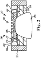
- Figure 2 is a section view illustrating an example of a printbar module 236 according to the present disclosure.
- a printbar 236 can be used in printer 134 shown in Figure 1 , according to an example implementation.
- the printbar illustrated in Figure 2 and Figure 8 is single printbar module, for example, formed after completion of as the process described with respect to Figure 11 .
- the elements described with respect to Figure 2 are analogous to those described with respect to Figure 3-8 .
- a portion of the dam 221 surrounding the recess 221 which would otherwise obscure the elements located behind the dam in the from the vantage of a section view has been purposefully omitted in an effort to clearly indicate the elements included in the Figures.
- the printbar 236 includes a PCB 214.
- the PCB 214 refers to a cured epoxy composition having conductive elements 213 (e.g., conductive signal traces and/or bond pads) included therein that can include particulate matter and/or structures (e.g., fiberglass structures, etc.) embedded in the epoxy, such as FR4 board.
- the PCB 214 is a continuous solid, as opposed to carrier boards that include prefabricated openings.
- the PCB 214 includes a recess 217.
- the recess 217 extends partially into the PCB 214, for example, as illustrated in Figure 3 .
- the recess 217 is included in a plurality of recesses that each extends partially into the PCB 214.
- the recess 217 (or the plurality of recesses), alone or in combination with other geometric feature(s) in the PCB 214 does not extend through the PCB 214 (e.g., does not extend completely through a total depth of).
- Formation of a recess 217 can include removal of a portion of the PCB 214 designated to become the recess and/or addition of material to the PCB 214 surrounding an area of the PCB designated to become the recess, among other methods of forming the recess.
- a recess such as recess 217
- the PCB 214 includes a dam 221 surrounding a perimeter of the recess 217.
- the dam is located as around (e.g., forming a perimeter) of an area of the PCB 214 designated to be the recess 217.
- Such added material can be the same or dissimilar to a material(s) include in the PCB 214 prior to adding the additional material.
- the additional material can, in some examples, include an additional epoxy layer of the same or dissimilar epoxy included in PCB 214 on which the additional material is placed.
- the recess 217 includes an adhesive material, such as adhesive material 215, on (e.g., disposed on) a bottom surface 219 of the recess 217.
- the adhesive material, such as adhesive material 215, refers to an epoxy, among other adhesive materials suitable to form the printbar modules, as described herein.
- the adhesive material can include a continuous adhesive material disposed on the bottom surface 219 of the recess 217. Such a continuous application may not be possible in PCB 14 having a prefabricated opening(s) as the adhesive material would undesirably migrate into the prefabricated opening(s). However, continuous application of the adhesive material in accordance with some examples of the present disclosure promotes die adhesion and/or provides mechanical stability of a resultant printbar module employing the same, among other advantages.
- Figure 2 illustrates the adhesive material 215 on the bottom surface 219 of the recess 217
- the adhesive material 215 can, advantageously be located on the bottom surface 219 of the recess 217 and at least a portion of a side surface (e.g., side surface 523 as illustrated in Figure 5 ) the printhead die sliver 212, among other locations to promote formation of the printbar modules 236.
- the adhesive material 215 can include adhesive material disposed on a surface (e.g., side surface 927 as illustrated in Figure 9 ) of the dam 221 surrounding the recess 217.
- Such application can promote at least a portion of a side surface of the printhead die sliver 212 having adhesive material 215 disposed therein, but is not vital to effectuate the same.
- the adhesive material 215 disposed on the surface of the dam 221 surrounding the recess 217 can be the same type of adhesive material 215 and/or can applied utilizing the same types of methods associated with applying adhesive material 215 to the bottom surface 219 of the PCB 214, as described herein.
- the conductive elements 213 of the PCB 214 can be coupled, for example by wire bonds 222, to electrical circuits included in a printhead die structure (not shown), as described herein.
- Conductive elements 213 are analogous to conductive elements 313, 413, 513, 613, 713, and 813 as illustrated in Figure 3, Figure 4, Figure 5 , Figure 6, Figure 7, and Figure 8 , respectively, similar to the other elements of Figure 2 and their respective analogous elements in Figures 3-8 .
- a molding 224 can encapsulate the wire bonds 222, the PCB 214, and/or the printhead die sliver 212.
- the molding 224 refers to a material that can protect the wire bonds 222, the PCB 214, and/or the printhead die sliver 212, such as an epoxy. Accordingly, such a molding can be applied and cured to protect the desired components.
- the molding can be a monolithic molding compound, for instance, enabling multiple rows of printhead die slivers to be molded in a single, monolithic body on the PCB 214.
- the PCB 214 includes a slot 216 form therein that extends through the PCB and an adhesive material 215 to the printhead die sliver 212.
- the slot 216 is not prefabricated and again advantageously promotes printhead die sliver 212 positioning and/or printhead die sliver adhesion, among other advantages. Formation of the slot is described in greater detail herein with respect to Figure 8 and with respect to Figure 11 .
- Figures 3 is a section view illustrating an example of a stage in a process of forming a printbar according to the present disclosure, for example, after providing a PCB as described with respect to Figure 11 .
- the PCB 314 can include a plurality of recesses, such as recess 317, extending partially through the PCB and/or a plurality of dams, such as dam 321, surrounding the plurality of recesses (e.g., as illustrated in Figure 9 ).
- the recess 317 can includes a bottom surface 319.
- Figure 4 is a section view illustrating an example of a stage subsequent to the stage illustrated in Figure 3 in a process of forming the printbar according to the present disclosure, for example, after applying an adhesive material to the PCB as described with respect to Figure 11 .
- applying adhesive material 415 to the PCB 414 can include applying adhesive material 415 only to each of the plurality of recesses of the PCB.
- adhesive material 415 can be applied only to a bottom surface 419 and/or side surfaces (e.g., side surface 27 as illustrated in Figure 9 ) of a dam 21 that form edges of the recess 17.
- Figure 5 is a section view illustrating an example of a stage subsequent to the stage illustrated in Figure 4 in a process of forming the printbar according to the present disclosure, for example, after positioning a die sliver in the recess as described with respect to Figure 11 .
- printhead die sliver 512 is positioned in an adhesive material 515 located on a bottom surface 519 of the recess having a dam 521 surrounding some/all of the recess.
- the adhesive material can be applied to a side surface 523 of the printhead die sliver 512, as described herein.
- Figure 6 is a section view illustrating an example of a stage subsequent to the stage illustrated in Figure 5 in a process of forming the printbar according to the present disclosure, for example, after bonding a die sliver with a PCB as described with respect to Figure 11 .
- Bonding as described herein, can include forming wire bonds 622 coupling conductive elements of the PCB 614 to conductive elements (not shown) of the printhead die sliver 612.
- Figure 7 is a section view illustrating an example of a stage subsequent to the stage illustrated in Figure 6 in a process of forming the printbar according to the present disclosure, after encapsulating a die sliver and/or a PCB with a molding as described with respect to Figure 11 . That is, molding 712 can, for example, encapsulate a printhead die sliver 712, wire bonds 722, and/or a PCB 714.
- Figure 8 is a section view illustrating an example of a stage subsequent to the stage illustrated in Figure 7 in a process of forming the printbar according to the present disclosure, after forming a slot extending through a PCB and an adhesive material (e.g., a portion of the adhesive material) to a printhead die sliver as described with respect to Figure 11 .
- an adhesive material e.g., a portion of the adhesive material
- a slot 816 is formed through the PCB 814 and the adhesive material 815 such that the slot 816 is in fluidic communication with an ink feed hole 825 included in the printhead die sliver 812.
- the slot can be formed using various techniques, such as laser etching, plunge-cut saw, and the like
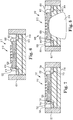
- FIG. 9 is a plan view illustrating a printbar according to the present disclosure.
- PCB 914 includes a plurality of recesses including recess 917.
- the recesses can be arranged in an end in a staggered configuration, among other possible configurations.
- the recess can include side surfaces, such as side surface 927. That is, each of the recesses includes side surfaces, such as side surface 927.
- an amount of adhesive material can be applied to a side surface 927 of dam 921.
- Side surface 927 can be flat, concave, or convex, among other possible shapes.
- An amount of adhesive material (not shown) sufficient to attach a side surface (e.g., side surface 523) of the printhead die to a side surface 927 of the dam 921 can, in some examples, be applied to the side surface 927.
- a resultant amount of adhesive material can be located between a side surface of the printhead die sliver and the side surface 927 of the dam 921 to promote printhead die sliver adhesion to a PCB 914 including the dam 921.
- Figure 10 is a plan view illustrating an example of a printbar according to the present disclosure.
- Printheads 1037 in PCB 1014, as illustrated in Figure 10 can be arranged in an end to end in rows 1048 in a staggered configuration in which the printheads in each row overlap another printhead in that row, among other possible configurations.
- each printhead 1037 includes a pair of printhead dies slivers 1012 each with two rows of ejection chambers (not shown) and corresponding orifices (not shown) through which printing fluid is ejected from the ejection chambers.
- Each slot form in the PCB 1014, as described herein, supplies printing fluid to one printhead die sliver 1012.
- printhead dies 1012 may be used with more or fewer ejection chambers and/or slots.
- Printing fluid flows into each ejection chamber from a manifold extending lengthwise along each printhead die, for example, between the two rows of ejection chambers.
- Printing fluid feeds into manifold through multiple ports that are connected to a slot at printhead die surface.
- Slot is substantially wider (at least twice as wide as) than printing fluid ports that carry printing fluid from larger, loosely spaced passages in and/or to the flow regulators or other parts that carry printing fluid into printbar to the smaller, tightly spaced printing fluid ports in printhead die.
- slot can help reduce or even eliminate a discrete "fan-out" and other fluid routing structures. That is, a separate fluidic fan-out structure is not included between the manifold and the printhead die slivers.
- exposing a substantial area of printhead die sliver surface e.g., an ink feed hole
- An actual printhead die sliver is typically a complex integrated circuit (IC) structure formed on a silicon substrate (not shown) with layers and elements not shown in Figs. 1-11 .
- IC integrated circuit
- a thermal ejector element or a piezoelectric ejector element (not shown) formed on the substrate at each ejection chamber (not shown) included in the printhead die sliver 12 is actuated to eject drops or streams of ink or other printing fluid from orifices (not shown).
- Figures 9 and 10 illustrate three staggered recesses, other suitable configurations are possible. For example, more or fewer printhead recesses may be used and/or the layout of the recesses may be altered. Similarly the shape, while illustrated as rectangular in nature, may be altered, for instance, depending upon the shape/size of a printhead die sliver and /or desired printbar module.
- Figure 10 shows a plan view of a printbar 1036 having staggered groups of printheads 1037 in the recesses of the PCB 14.
- Each of the groups includes four printheads 1037 by way of example, although a group can have more or less printheads.
- Figure 11 is a flow diagram of a process of forming a printbar according to the present disclosure.
- the method includes providing a PCB including a plurality of recesses extending partially through the PCB and a plurality of dams surrounding the plurality of recesses.
- Providing includes forming the plurality of recesses and/or the plurality of dams in the PCB.
- the PCB can include prefabricated recesses and/or dams.
- a PCB including prefabricated recesses extending partially through the PCB and/or dams surrounding at least a portion of the recesses can be provided.
- Such a PCB, recesses, and/or dams can be analogous to the PCB as described with respect to Figures 1-10 .
- Adhesive material can be applied to the PCB.
- the method includes applying an adhesive material to each of the plurality of recesses, as shown at 1191.
- the adhesive material include a flowable thermoset epoxy, among other adhesive materials suitable for application and printhead modules, as described herein.
- the adhesive material is applied to provide permanent adhesion of the die slivers to the PCB, as opposed to temporary adhesive material(s)/temporary adhesive products, for instance, temporary adhesion associated with thermal release tape and/or ultraviolet release tape, among other temporary adhesives materials and/or products utilizing temporary adhesive materials.
- the adhesive material is applied on both a bottom surface of the recess and/or side surfaces of a dam (e.g., surfaces of the adhesive material in contact with a side surface of the dam), such that, the adhesive material can attach a printhead die sliver to the PCB.
- the adhesive material can be applied (e.g., continuously applied) to a bottom surface of each of the plurality of recesses and/or applied to a side surface (e.g., side surface as illustrated in Figure 9 ) of the dam adjacent the plurality of recesses.
- an amount of adhesive material sufficient to enable the adhesive material to attach to a side surface of the printhead die and/or a side surface of the dam can be applied.
- the adhesive material can be applied to the plurality of recesses and/or applied to a side surfaces of the dam using various techniques such as adhesive material stamping, stencil printing, and/or pin transfer, among other suitable techniques to apply the adhesive material as described herein.
- applying adhesive material to the PCB includes applying adhesive material only to each of the plurality of recesses of the PCB. Such limited application can promote die positioning and/or provide a comparative reduction in cost associated with adhesive application (e.g., compared to coating the entire PCB), among other advantages.
- the adhesive material can be applied in a thickness and/or pattern suitable to promote positioning of the printhead die slivers.
- the method includes positioning a plurality of printhead die slivers in the plurality of recesses, as illustrated at 1192. Positioning can, in some examples, positioning the plurality of printhead die slivers within an adhesive material, such as adhesive material applied at 1191.
- the plurality of die slivers can be positioned with an orifice side facing down (towards a bottom surface of a recess) in the plurality of recesses.
- One of more of the plurality of die slivers can be positioned with each of the plurality of recesses.
- a single die sliver of the plurality of die slivers is positioned within a single recess of the plurality of recesses.
- a total number of the die slivers positioned in the recesses can equal a total number of the plurality of recesses.
- other positioning arrangements and/or total number of the plurality of printhead die slivers relative to a total number of the plurality of recesses are possible depending upon a desired type/performance of a resultant printbar module.
- the method includes bonding the plurality of printhead die slivers with the PCB.
- the plurality of printhead die slivers positioned in the plurality of recesses, as illustrated at 1192, are bonded to the PCB.
- Bonding can, in some examples, include wire bonds coupling conductive elements, such as conductive elements, of the PCB to conductive elements of the printhead die slivers.
- Wire bonds can include gold and/or copper bonds, among other suitable materials for forming wire bonds, for example, ball bond or wedge bonds coupling conductive elements of the PCB to conductive elements of the printhead die slivers.
- the method includes encapsulating the plurality of printhead die slivers and/or the PCB with a molding, as illustrated at 1194.
- the mold can partially and/or completely encapsulate the plurality of printhead die slivers.
- the plurality of printhead die slivers and/or the PCB can be encapsulated with a molding in response to bonding the plurality of printhead die slivers with the PCB.
- Encapsulating can include dispensing a liquid encapsulate material (e.g., an epoxy and/or an epoxy-based encapsulate material) over the printhead die slivers and/or and the wire bonds.
- a liquid encapsulate material e.g., an epoxy and/or an epoxy-based encapsulate material
- encapsulating can planarize the printhead die sliver, for instance, making a top surface of the printhead die sliver (e.g., a top surface of the molding located above a top surface of the printhead die sliver) co-planar with a top surface of a dam.
- a top surface of the printhead die sliver e.g., a top surface of the molding located above a top surface of the printhead die sliver
- the method includes forming a plurality of slots, extending through the PCB and the adhesive material, as illustrated at 1195. That is, the plurality of slots is formed after completion of encapsulating, as described herein.
- the plurality of slots are in fluidic communication with fluid (e.g., ink) feed holes of the plurality of printhead die slivers to provide direct fluidic communication without fan-out, as described herein.
- the adhesive material can remain on the bottom surface of the recess and a bottom surface of each of the plurality of printhead die slivers and/or between a side surface of the plurality of die slivers and a side surface(s) of a dam(s), such as dam.
- forming can include forming the plurality of slots such that a portion of the adhesive material remains between the bottom surface 19 of the recess and a bottom surface of each of the plurality of printhead die slivers.
- forming includes forming the plurality of slots using a plunge-cut saw.
- forming the plurality of slots can employ suitable chemical (e.g., chemical etching, etc.) and/or mechanical (e.g., drill, sandblasting, laser, etc.) methods to form the plurality of slots.
- the plurality of die slivers including printhead die sliver are not part of a single semiconductor substrate, but rather are formed from separate semiconductor substrates (note that the plurality of slivers can be formed on a single PCB and then singulated during manufacture to be assembled as part of printer).
- the separate printhead die slivers can be positioned to provide an appropriate ink slot pitch that cooperates with a manifold (not shown) to receive the ink.
- a width of each die sliver can be substantially narrower than a spacing between die slivers.
- the thickness of each die sliver can be substantially thinner than a thickness of the PCB and/or a molding.
- each die sliver is less than or equal to 300 micrometers. It is to be understood that the die slivers can have other thickness more than 300 micrometers.
- a "micro device” means a device having at least one exterior dimensions less than or equal to 30mm; "thin” means a thickness less than or equal to 650 ⁇ m; a “sliver” means a thin micro device having a ratio of length to width (L/W) of at least three; a "printhead” and a “printhead die” mean that part of an inkjet printer or other inkjet type dispenser that dispenses fluid from at least one openings.
- a printhead includes at least one printhead dies.
- “Printhead” and “printhead die sliver” are not limited to printing with ink and other printing fluids but also include inkjet type dispensing of other fluids and/or for uses other than printing.
- printbar and "printbar module” as used herein is meant to encompass various print structures, such as page-wide modules, integrated printhead/containers, individual ink cartridges, and the like. While the present disclosures describes “ink” by way of example, it is to be understood that “fluid” can be used in place of “ink” wherever “ink” is specifically recited.
Landscapes
- Engineering & Computer Science (AREA)
- Manufacturing & Machinery (AREA)
- Particle Formation And Scattering Control In Inkjet Printers (AREA)
Claims (14)
- Module de barre d'impression comprenant :une carte de circuits imprimés (PCB) (214) comportant une pluralité d'évidements (217) qui s'étendent partiellement dans la PCB, dans lequel chaque évidement (217) comporte un matériau adhésif (215) sur une surface inférieure (219) de l'évidement (217) ;un ruban de matrice de tête d'impression (212) positionné dans chaque évidement (217), dans lequel chaque ruban de matrice de tête d'impression comporte une pluralité de rangées de chambres d'éjection et d'orifices correspondants à travers lesquels le fluide d'impression est éjecté des chambres d'éjection et une pluralité de trous d'alimentation en fluide ; et une pluralité de rainures (216) s'étendant à travers la PCB (214) et le matériau adhésif (215) jusqu'aux rubans de matrice de tête d'impression (212), dans lequel chaque rainure est en communication fluidique avec les trous d'alimentation en fluide de l'un des rubans de matrice de tête d'impression dans lequel la rainure est formée à travers la PCB et le matériau adhésif après que le ruban de matrice de tête d'impression est positionné dans l'évidement.
- Module de barre d'impression selon la revendication 1, dans lequel la PCB ne comporte pas d'ouverture préfabriquée s'étendant à travers la PCB.
- Module de barre d'impression selon la revendication 1, dans lequel chaque évidement est formé par une digue ajoutée à la PCB, la digue (221) entourant un périmètre de chaque évidement.
- Module de barre d'impression selon la revendication 1, dans lequel chaque évidement est formé par enlèvement d'une partie du matériau de la PCB.
- Module de barre d'impression selon la revendication 3, dans lequel une surface supérieure de chaque ruban de matrice de tête d'impression (212) est coplanaire avec une surface supérieure de la digue (221).
- Module de barre d'impression selon la revendication 1, dans lequel chacun des évidements ne s'étend pas à travers la PCB.
- Module de barre d'impression selon la revendication 1, dans lequel chaque ruban de matrice de tête d'impression (212) est positionné de sorte que le matériau adhésif (215) recouvre une surface inférieure et au moins une partie d'une surface latérale du ruban de matrice de tête d'impression (212).
- Module de barre d'impression selon la revendication 1, dans lequel le matériau adhésif (215) comporte un matériau adhésif continu disposé sur la surface inférieure (219) de chaque évidement (217).
- Module de barre d'impression selon la revendication 3, dans lequel le matériau adhésif (215) comporte un matériau adhésif disposé sur une surface de la digue (221) entourant chaque évidement (217).
- Procédé de formation d'un module de barre d'impression, comprenant :la fourniture d'une carte de circuits imprimés (PCB) (214) comportant une pluralité d'évidements (217) s'étendant partiellement à travers la PCB (214) et une pluralité de digues (221) entourant la pluralité d'évidements (217) ;l'application d'un matériau adhésif (215) à chacun de la pluralité d'évidements (217) ;le positionnement d'une pluralité de rubans de matrice de tête d'impression (212) dans la pluralité d'évidements (217), chacun de la pluralité de rubans de matrice de tête d'impression comportant une pluralité de rangées de chambres d'éjection et d'orifices correspondants à travers lesquels le fluide d'impression est éjecté des chambres d'éjection et une pluralité de trous d'alimentation en fluide ;la collage de la pluralité de rubans de matrice de tête d'impression avec la PCB ;l'encapsulation de la pluralité de rubans de matrice de tête d'impression (212) et la PCB (214) avec un moulage ; etaprès l'encapsulation, la formation d'une pluralité de rainures, s'étendant à travers la PCB (214) et le matériau adhésif (215), dans lequel chaque rainure est en communication fluidique avec des trous d'alimentation en fluide de l'un des rubans de matrice de tête d'impression (212) pour fournir une communication fluidique directe sans sortance.
- Procédé selon la revendication 10, dans lequel la formation comprend la formation de la pluralité de rainures (216) à l'aide d'une scie plongeante.
- Procédé selon la revendication 10, dans lequel la liaison comporte des plots de fils (222) couplant les éléments conducteurs de la PCB (214) aux éléments conducteurs des rubans de matrice de tête d'impression (212).
- Procédé selon la revendication 10, dans lequel l'application du matériau adhésif (215) sur la PCB (214) comporte l'application du matériau adhésif (215) uniquement à chacun de la pluralité d'évidements (217) de la PCB.
- Procédé selon la revendication 10, dans lequel la formation comporte la formation de la pluralité de rainures (216) de sorte qu'une partie du matériau adhésif (215) reste entre la surface inférieure (219) de l'évidement (217) et une surface inférieure de chacun de la pluralité de rubans de matrice de tête d'impression (212).
Applications Claiming Priority (1)
| Application Number | Priority Date | Filing Date | Title |
|---|---|---|---|
| PCT/US2014/013317 WO2015116027A1 (fr) | 2014-01-28 | 2014-01-28 | Barres d'impression et procédés de formation de barres d'impression |
Publications (3)
| Publication Number | Publication Date |
|---|---|
| EP3099493A1 EP3099493A1 (fr) | 2016-12-07 |
| EP3099493A4 EP3099493A4 (fr) | 2017-09-27 |
| EP3099493B1 true EP3099493B1 (fr) | 2020-05-06 |
Family
ID=53757442
Family Applications (1)
| Application Number | Title | Priority Date | Filing Date |
|---|---|---|---|
| EP14881051.8A Not-in-force EP3099493B1 (fr) | 2014-01-28 | 2014-01-28 | Barres d'impression et procédés de formation de barres d'impression |
Country Status (4)
| Country | Link |
|---|---|
| US (3) | US10421274B2 (fr) |
| EP (1) | EP3099493B1 (fr) |
| CN (1) | CN105939855B (fr) |
| WO (1) | WO2015116027A1 (fr) |
Families Citing this family (11)
| Publication number | Priority date | Publication date | Assignee | Title |
|---|---|---|---|---|
| BR112015020862B1 (pt) | 2013-02-28 | 2021-05-25 | Hewlett-Packard Development Company, L.P. | barra de impressão moldada |
| US9656469B2 (en) | 2013-02-28 | 2017-05-23 | Hewlett-Packard Development Company, L.P. | Molded fluid flow structure with saw cut channel |
| US10821729B2 (en) | 2013-02-28 | 2020-11-03 | Hewlett-Packard Development Company, L.P. | Transfer molded fluid flow structure |
| EP2961612B1 (fr) | 2013-02-28 | 2019-08-07 | Hewlett-Packard Development Company, L.P. | Moulage d'une structure d'écoulement de fluide |
| US9724920B2 (en) * | 2013-03-20 | 2017-08-08 | Hewlett-Packard Development Company, L.P. | Molded die slivers with exposed front and back surfaces |
| US10421274B2 (en) * | 2014-01-28 | 2019-09-24 | Hewlett-Packard Devleopment Company. L.P. | Printbars and methods of forming printbars |
| EP3362292B1 (fr) * | 2015-10-15 | 2022-03-09 | Hewlett-Packard Development Company, L.P. | Tête d'impression moulée comprenant un interposeur et procédé de fabrication d'une tête d'impression moulée comprenant un interposeur |
| CN110891793B (zh) | 2017-07-31 | 2021-04-09 | 惠普发展公司,有限责任合伙企业 | 具有封闭式横向通道的流体喷射管芯 |
| CN110891792B (zh) | 2017-07-31 | 2021-06-01 | 惠普发展公司,有限责任合伙企业 | 具有封闭式横向通道的流体喷射装置 |
| WO2021201822A1 (fr) * | 2020-03-30 | 2021-10-07 | Hewlett-Packard Development Company, L.P. | Ensembles d'éjection de fluide |
| CN116135539B (zh) * | 2021-11-18 | 2025-07-11 | 深圳弘锐精密数码喷印设备有限公司 | 一种白油块的喷印方法及数码喷印设备 |
Family Cites Families (28)
| Publication number | Priority date | Publication date | Assignee | Title |
|---|---|---|---|---|
| US4528577A (en) * | 1982-11-23 | 1985-07-09 | Hewlett-Packard Co. | Ink jet orifice plate having integral separators |
| US6106096A (en) | 1997-12-15 | 2000-08-22 | Lexmark International, Inc. | Printhead stress relief |
| US6273557B1 (en) * | 1998-03-02 | 2001-08-14 | Hewlett-Packard Company | Micromachined ink feed channels for an inkjet printhead |
| US6379988B1 (en) | 2000-05-16 | 2002-04-30 | Sandia Corporation | Pre-release plastic packaging of MEMS and IMEMS devices |
| US6481832B2 (en) * | 2001-01-29 | 2002-11-19 | Hewlett-Packard Company | Fluid-jet ejection device |
| US6548895B1 (en) * | 2001-02-21 | 2003-04-15 | Sandia Corporation | Packaging of electro-microfluidic devices |
| US6554399B2 (en) | 2001-02-27 | 2003-04-29 | Hewlett-Packard Development Company, L.P. | Interconnected printhead die and carrier substrate system |
| US7125731B2 (en) | 2001-10-31 | 2006-10-24 | Hewlett-Packard Development Company, L.P. | Drop generator for ultra-small droplets |
| US6631979B2 (en) | 2002-01-17 | 2003-10-14 | Eastman Kodak Company | Thermal actuator with optimized heater length |
| CN1490160A (zh) | 2002-10-16 | 2004-04-21 | 飞赫科技股份有限公司 | 压电喷墨头及其压力腔成型法 |
| JP4468751B2 (ja) * | 2004-06-30 | 2010-05-26 | 富士重工業株式会社 | 水平軸風車およびその待機方法 |
| US7475964B2 (en) * | 2004-08-06 | 2009-01-13 | Hewlett-Packard Development Company, L.P. | Electrical contact encapsulation |
| US7105456B2 (en) * | 2004-10-29 | 2006-09-12 | Hewlett-Packard Development Company, Lp. | Methods for controlling feature dimensions in crystalline substrates |
| US7828417B2 (en) * | 2007-04-23 | 2010-11-09 | Hewlett-Packard Development Company, L.P. | Microfluidic device and a fluid ejection device incorporating the same |
| JP5008451B2 (ja) * | 2007-05-08 | 2012-08-22 | キヤノン株式会社 | 液体吐出ヘッド及び液体吐出ヘッドの製造方法 |
| US7681991B2 (en) * | 2007-06-04 | 2010-03-23 | Lexmark International, Inc. | Composite ceramic substrate for micro-fluid ejection head |
| US8109607B2 (en) * | 2008-03-10 | 2012-02-07 | Hewlett-Packard Development Company, L.P. | Fluid ejector structure and fabrication method |
| US7862147B2 (en) | 2008-09-30 | 2011-01-04 | Eastman Kodak Company | Inclined feature to protect printhead face |
| US8496317B2 (en) * | 2009-08-11 | 2013-07-30 | Eastman Kodak Company | Metalized printhead substrate overmolded with plastic |
| US8622524B2 (en) | 2010-05-27 | 2014-01-07 | Funai Electric Co., Ltd. | Laminate constructs for micro-fluid ejection devices |
| US20110298868A1 (en) | 2010-06-07 | 2011-12-08 | Silverbrook Research Pty Ltd | Inkjet printhead having hydrophilic ink pathways |
| JP2013028110A (ja) * | 2011-07-29 | 2013-02-07 | Canon Inc | 液体吐出ヘッド用基板の製造方法 |
| US8887393B2 (en) * | 2012-01-27 | 2014-11-18 | Eastman Kodak Company | Fabrication of an inkjet printhead mounting substrate |
| US8690296B2 (en) | 2012-01-27 | 2014-04-08 | Eastman Kodak Company | Inkjet printhead with multi-layer mounting substrate |
| US9539814B2 (en) * | 2013-02-28 | 2017-01-10 | Hewlett-Packard Development Company, L.P. | Molded printhead |
| US9517626B2 (en) * | 2013-02-28 | 2016-12-13 | Hewlett-Packard Development Company, L.P. | Printed circuit board fluid ejection apparatus |
| CN105555539B (zh) | 2013-09-20 | 2017-08-15 | 惠普发展公司,有限责任合伙企业 | 打印杆以及形成打印杆的方法 |
| US10421274B2 (en) * | 2014-01-28 | 2019-09-24 | Hewlett-Packard Devleopment Company. L.P. | Printbars and methods of forming printbars |
-
2014
- 2014-01-28 US US15/113,533 patent/US10421274B2/en not_active Expired - Fee Related
- 2014-01-28 WO PCT/US2014/013317 patent/WO2015116027A1/fr not_active Ceased
- 2014-01-28 EP EP14881051.8A patent/EP3099493B1/fr not_active Not-in-force
- 2014-01-28 CN CN201480074324.8A patent/CN105939855B/zh not_active Expired - Fee Related
-
2018
- 2018-01-31 US US15/885,458 patent/US10226926B2/en not_active Expired - Fee Related
-
2019
- 2019-08-15 US US16/541,410 patent/US10780696B2/en not_active Expired - Fee Related
Non-Patent Citations (1)
| Title |
|---|
| None * |
Also Published As
| Publication number | Publication date |
|---|---|
| US20170008281A1 (en) | 2017-01-12 |
| US20180154633A1 (en) | 2018-06-07 |
| US20200023641A1 (en) | 2020-01-23 |
| EP3099493A4 (fr) | 2017-09-27 |
| US10421274B2 (en) | 2019-09-24 |
| EP3099493A1 (fr) | 2016-12-07 |
| WO2015116027A1 (fr) | 2015-08-06 |
| US10780696B2 (en) | 2020-09-22 |
| CN105939855A (zh) | 2016-09-14 |
| CN105939855B (zh) | 2017-09-05 |
| US10226926B2 (en) | 2019-03-12 |
Similar Documents
| Publication | Publication Date | Title |
|---|---|---|
| US10780696B2 (en) | Printbars and methods of forming printbars | |
| US11292257B2 (en) | Molded die slivers with exposed front and back surfaces | |
| EP3046768B1 (fr) | Barre d'impression et son procédé de formation | |
| US10300701B2 (en) | Printed circuit board fluid ejection apparatus | |
| CN107901609B (zh) | 流体流动结构和打印头 | |
| US10479086B2 (en) | Process for making a molded device assembly and printhead assembly | |
| US10232621B2 (en) | Process for making a molded device assembly and printhead assembly | |
| EP2976221B1 (fr) | Rubans de filière moulés ayant des surfaces avant et arrière exposées | |
| US10220620B2 (en) | Molded printhead structure | |
| US9517626B2 (en) | Printed circuit board fluid ejection apparatus | |
| TWI624380B (zh) | 包括具暴露前與後表面之模製晶粒條片的列印頭、列印條及列印卡匣 |
Legal Events
| Date | Code | Title | Description |
|---|---|---|---|
| PUAI | Public reference made under article 153(3) epc to a published international application that has entered the european phase |
Free format text: ORIGINAL CODE: 0009012 |
|
| STAA | Information on the status of an ep patent application or granted ep patent |
Free format text: STATUS: REQUEST FOR EXAMINATION WAS MADE |
|
| 17P | Request for examination filed |
Effective date: 20160708 |
|
| AK | Designated contracting states |
Kind code of ref document: A1 Designated state(s): AL AT BE BG CH CY CZ DE DK EE ES FI FR GB GR HR HU IE IS IT LI LT LU LV MC MK MT NL NO PL PT RO RS SE SI SK SM TR |
|
| AX | Request for extension of the european patent |
Extension state: BA ME |
|
| DAX | Request for extension of the european patent (deleted) | ||
| A4 | Supplementary search report drawn up and despatched |
Effective date: 20170830 |
|
| RIC1 | Information provided on ipc code assigned before grant |
Ipc: B41J 29/38 20060101ALI20170824BHEP Ipc: B41J 2/04 20060101AFI20170824BHEP |
|
| RAP1 | Party data changed (applicant data changed or rights of an application transferred) |
Owner name: HEWLETT-PACKARD DEVELOPMENT COMPANY, L.P. |
|
| REG | Reference to a national code |
Ref country code: DE Ref legal event code: R079 Ref document number: 602014065279 Country of ref document: DE Free format text: PREVIOUS MAIN CLASS: B41J0002040000 Ipc: B41J0002160000 |
|
| GRAP | Despatch of communication of intention to grant a patent |
Free format text: ORIGINAL CODE: EPIDOSNIGR1 |
|
| STAA | Information on the status of an ep patent application or granted ep patent |
Free format text: STATUS: GRANT OF PATENT IS INTENDED |
|
| RIC1 | Information provided on ipc code assigned before grant |
Ipc: B41J 2/16 20060101AFI20191212BHEP |
|
| INTG | Intention to grant announced |
Effective date: 20200110 |
|
| GRAS | Grant fee paid |
Free format text: ORIGINAL CODE: EPIDOSNIGR3 |
|
| GRAA | (expected) grant |
Free format text: ORIGINAL CODE: 0009210 |
|
| STAA | Information on the status of an ep patent application or granted ep patent |
Free format text: STATUS: THE PATENT HAS BEEN GRANTED |
|
| AK | Designated contracting states |
Kind code of ref document: B1 Designated state(s): AL AT BE BG CH CY CZ DE DK EE ES FI FR GB GR HR HU IE IS IT LI LT LU LV MC MK MT NL NO PL PT RO RS SE SI SK SM TR |
|
| REG | Reference to a national code |
Ref country code: GB Ref legal event code: FG4D |
|
| REG | Reference to a national code |
Ref country code: AT Ref legal event code: REF Ref document number: 1266145 Country of ref document: AT Kind code of ref document: T Effective date: 20200515 Ref country code: CH Ref legal event code: EP |
|
| REG | Reference to a national code |
Ref country code: IE Ref legal event code: FG4D |
|
| REG | Reference to a national code |
Ref country code: DE Ref legal event code: R096 Ref document number: 602014065279 Country of ref document: DE |
|
| REG | Reference to a national code |
Ref country code: LT Ref legal event code: MG4D |
|
| REG | Reference to a national code |
Ref country code: NL Ref legal event code: MP Effective date: 20200506 |
|
| PG25 | Lapsed in a contracting state [announced via postgrant information from national office to epo] |
Ref country code: GR Free format text: LAPSE BECAUSE OF FAILURE TO SUBMIT A TRANSLATION OF THE DESCRIPTION OR TO PAY THE FEE WITHIN THE PRESCRIBED TIME-LIMIT Effective date: 20200807 Ref country code: LT Free format text: LAPSE BECAUSE OF FAILURE TO SUBMIT A TRANSLATION OF THE DESCRIPTION OR TO PAY THE FEE WITHIN THE PRESCRIBED TIME-LIMIT Effective date: 20200506 Ref country code: IS Free format text: LAPSE BECAUSE OF FAILURE TO SUBMIT A TRANSLATION OF THE DESCRIPTION OR TO PAY THE FEE WITHIN THE PRESCRIBED TIME-LIMIT Effective date: 20200906 Ref country code: FI Free format text: LAPSE BECAUSE OF FAILURE TO SUBMIT A TRANSLATION OF THE DESCRIPTION OR TO PAY THE FEE WITHIN THE PRESCRIBED TIME-LIMIT Effective date: 20200506 Ref country code: NO Free format text: LAPSE BECAUSE OF FAILURE TO SUBMIT A TRANSLATION OF THE DESCRIPTION OR TO PAY THE FEE WITHIN THE PRESCRIBED TIME-LIMIT Effective date: 20200806 Ref country code: PT Free format text: LAPSE BECAUSE OF FAILURE TO SUBMIT A TRANSLATION OF THE DESCRIPTION OR TO PAY THE FEE WITHIN THE PRESCRIBED TIME-LIMIT Effective date: 20200907 Ref country code: SE Free format text: LAPSE BECAUSE OF FAILURE TO SUBMIT A TRANSLATION OF THE DESCRIPTION OR TO PAY THE FEE WITHIN THE PRESCRIBED TIME-LIMIT Effective date: 20200506 |
|
| PG25 | Lapsed in a contracting state [announced via postgrant information from national office to epo] |
Ref country code: HR Free format text: LAPSE BECAUSE OF FAILURE TO SUBMIT A TRANSLATION OF THE DESCRIPTION OR TO PAY THE FEE WITHIN THE PRESCRIBED TIME-LIMIT Effective date: 20200506 Ref country code: BG Free format text: LAPSE BECAUSE OF FAILURE TO SUBMIT A TRANSLATION OF THE DESCRIPTION OR TO PAY THE FEE WITHIN THE PRESCRIBED TIME-LIMIT Effective date: 20200806 Ref country code: RS Free format text: LAPSE BECAUSE OF FAILURE TO SUBMIT A TRANSLATION OF THE DESCRIPTION OR TO PAY THE FEE WITHIN THE PRESCRIBED TIME-LIMIT Effective date: 20200506 Ref country code: LV Free format text: LAPSE BECAUSE OF FAILURE TO SUBMIT A TRANSLATION OF THE DESCRIPTION OR TO PAY THE FEE WITHIN THE PRESCRIBED TIME-LIMIT Effective date: 20200506 |
|
| REG | Reference to a national code |
Ref country code: AT Ref legal event code: MK05 Ref document number: 1266145 Country of ref document: AT Kind code of ref document: T Effective date: 20200506 |
|
| PG25 | Lapsed in a contracting state [announced via postgrant information from national office to epo] |
Ref country code: AL Free format text: LAPSE BECAUSE OF FAILURE TO SUBMIT A TRANSLATION OF THE DESCRIPTION OR TO PAY THE FEE WITHIN THE PRESCRIBED TIME-LIMIT Effective date: 20200506 Ref country code: NL Free format text: LAPSE BECAUSE OF FAILURE TO SUBMIT A TRANSLATION OF THE DESCRIPTION OR TO PAY THE FEE WITHIN THE PRESCRIBED TIME-LIMIT Effective date: 20200506 |
|
| PG25 | Lapsed in a contracting state [announced via postgrant information from national office to epo] |
Ref country code: ES Free format text: LAPSE BECAUSE OF FAILURE TO SUBMIT A TRANSLATION OF THE DESCRIPTION OR TO PAY THE FEE WITHIN THE PRESCRIBED TIME-LIMIT Effective date: 20200506 Ref country code: DK Free format text: LAPSE BECAUSE OF FAILURE TO SUBMIT A TRANSLATION OF THE DESCRIPTION OR TO PAY THE FEE WITHIN THE PRESCRIBED TIME-LIMIT Effective date: 20200506 Ref country code: AT Free format text: LAPSE BECAUSE OF FAILURE TO SUBMIT A TRANSLATION OF THE DESCRIPTION OR TO PAY THE FEE WITHIN THE PRESCRIBED TIME-LIMIT Effective date: 20200506 Ref country code: EE Free format text: LAPSE BECAUSE OF FAILURE TO SUBMIT A TRANSLATION OF THE DESCRIPTION OR TO PAY THE FEE WITHIN THE PRESCRIBED TIME-LIMIT Effective date: 20200506 Ref country code: SM Free format text: LAPSE BECAUSE OF FAILURE TO SUBMIT A TRANSLATION OF THE DESCRIPTION OR TO PAY THE FEE WITHIN THE PRESCRIBED TIME-LIMIT Effective date: 20200506 Ref country code: CZ Free format text: LAPSE BECAUSE OF FAILURE TO SUBMIT A TRANSLATION OF THE DESCRIPTION OR TO PAY THE FEE WITHIN THE PRESCRIBED TIME-LIMIT Effective date: 20200506 Ref country code: RO Free format text: LAPSE BECAUSE OF FAILURE TO SUBMIT A TRANSLATION OF THE DESCRIPTION OR TO PAY THE FEE WITHIN THE PRESCRIBED TIME-LIMIT Effective date: 20200506 Ref country code: IT Free format text: LAPSE BECAUSE OF FAILURE TO SUBMIT A TRANSLATION OF THE DESCRIPTION OR TO PAY THE FEE WITHIN THE PRESCRIBED TIME-LIMIT Effective date: 20200506 |
|
| REG | Reference to a national code |
Ref country code: DE Ref legal event code: R097 Ref document number: 602014065279 Country of ref document: DE |
|
| PG25 | Lapsed in a contracting state [announced via postgrant information from national office to epo] |
Ref country code: SK Free format text: LAPSE BECAUSE OF FAILURE TO SUBMIT A TRANSLATION OF THE DESCRIPTION OR TO PAY THE FEE WITHIN THE PRESCRIBED TIME-LIMIT Effective date: 20200506 Ref country code: PL Free format text: LAPSE BECAUSE OF FAILURE TO SUBMIT A TRANSLATION OF THE DESCRIPTION OR TO PAY THE FEE WITHIN THE PRESCRIBED TIME-LIMIT Effective date: 20200506 |
|
| PLBE | No opposition filed within time limit |
Free format text: ORIGINAL CODE: 0009261 |
|
| STAA | Information on the status of an ep patent application or granted ep patent |
Free format text: STATUS: NO OPPOSITION FILED WITHIN TIME LIMIT |
|
| 26N | No opposition filed |
Effective date: 20210209 |
|
| PG25 | Lapsed in a contracting state [announced via postgrant information from national office to epo] |
Ref country code: SI Free format text: LAPSE BECAUSE OF FAILURE TO SUBMIT A TRANSLATION OF THE DESCRIPTION OR TO PAY THE FEE WITHIN THE PRESCRIBED TIME-LIMIT Effective date: 20200506 |
|
| PG25 | Lapsed in a contracting state [announced via postgrant information from national office to epo] |
Ref country code: MC Free format text: LAPSE BECAUSE OF FAILURE TO SUBMIT A TRANSLATION OF THE DESCRIPTION OR TO PAY THE FEE WITHIN THE PRESCRIBED TIME-LIMIT Effective date: 20200506 |
|
| REG | Reference to a national code |
Ref country code: CH Ref legal event code: PL |
|
| PG25 | Lapsed in a contracting state [announced via postgrant information from national office to epo] |
Ref country code: LU Free format text: LAPSE BECAUSE OF NON-PAYMENT OF DUE FEES Effective date: 20210128 |
|
| REG | Reference to a national code |
Ref country code: BE Ref legal event code: MM Effective date: 20210131 |
|
| PG25 | Lapsed in a contracting state [announced via postgrant information from national office to epo] |
Ref country code: CH Free format text: LAPSE BECAUSE OF NON-PAYMENT OF DUE FEES Effective date: 20210131 Ref country code: LI Free format text: LAPSE BECAUSE OF NON-PAYMENT OF DUE FEES Effective date: 20210131 |
|
| PG25 | Lapsed in a contracting state [announced via postgrant information from national office to epo] |
Ref country code: IE Free format text: LAPSE BECAUSE OF NON-PAYMENT OF DUE FEES Effective date: 20210128 |
|
| PGFP | Annual fee paid to national office [announced via postgrant information from national office to epo] |
Ref country code: GB Payment date: 20211216 Year of fee payment: 9 Ref country code: FR Payment date: 20211215 Year of fee payment: 9 |
|
| PGFP | Annual fee paid to national office [announced via postgrant information from national office to epo] |
Ref country code: DE Payment date: 20211215 Year of fee payment: 9 |
|
| PG25 | Lapsed in a contracting state [announced via postgrant information from national office to epo] |
Ref country code: BE Free format text: LAPSE BECAUSE OF NON-PAYMENT OF DUE FEES Effective date: 20210131 |
|
| PG25 | Lapsed in a contracting state [announced via postgrant information from national office to epo] |
Ref country code: HU Free format text: LAPSE BECAUSE OF FAILURE TO SUBMIT A TRANSLATION OF THE DESCRIPTION OR TO PAY THE FEE WITHIN THE PRESCRIBED TIME-LIMIT; INVALID AB INITIO Effective date: 20140128 |
|
| PG25 | Lapsed in a contracting state [announced via postgrant information from national office to epo] |
Ref country code: CY Free format text: LAPSE BECAUSE OF FAILURE TO SUBMIT A TRANSLATION OF THE DESCRIPTION OR TO PAY THE FEE WITHIN THE PRESCRIBED TIME-LIMIT Effective date: 20200506 |
|
| REG | Reference to a national code |
Ref country code: DE Ref legal event code: R119 Ref document number: 602014065279 Country of ref document: DE |
|
| GBPC | Gb: european patent ceased through non-payment of renewal fee |
Effective date: 20230128 |
|
| PG25 | Lapsed in a contracting state [announced via postgrant information from national office to epo] |
Ref country code: GB Free format text: LAPSE BECAUSE OF NON-PAYMENT OF DUE FEES Effective date: 20230128 Ref country code: DE Free format text: LAPSE BECAUSE OF NON-PAYMENT OF DUE FEES Effective date: 20230801 |
|
| PG25 | Lapsed in a contracting state [announced via postgrant information from national office to epo] |
Ref country code: FR Free format text: LAPSE BECAUSE OF NON-PAYMENT OF DUE FEES Effective date: 20230131 |
|
| PG25 | Lapsed in a contracting state [announced via postgrant information from national office to epo] |
Ref country code: MK Free format text: LAPSE BECAUSE OF FAILURE TO SUBMIT A TRANSLATION OF THE DESCRIPTION OR TO PAY THE FEE WITHIN THE PRESCRIBED TIME-LIMIT Effective date: 20200506 |
|
| PG25 | Lapsed in a contracting state [announced via postgrant information from national office to epo] |
Ref country code: TR Free format text: LAPSE BECAUSE OF FAILURE TO SUBMIT A TRANSLATION OF THE DESCRIPTION OR TO PAY THE FEE WITHIN THE PRESCRIBED TIME-LIMIT Effective date: 20200506 |
|
| PG25 | Lapsed in a contracting state [announced via postgrant information from national office to epo] |
Ref country code: MT Free format text: LAPSE BECAUSE OF FAILURE TO SUBMIT A TRANSLATION OF THE DESCRIPTION OR TO PAY THE FEE WITHIN THE PRESCRIBED TIME-LIMIT Effective date: 20200506 |