EP3100032B1 - Appareil et procédé pour l'inspection combinée en champ clair, en champ sombre et photothermique - Google Patents
Appareil et procédé pour l'inspection combinée en champ clair, en champ sombre et photothermique Download PDFInfo
- Publication number
- EP3100032B1 EP3100032B1 EP15749379.2A EP15749379A EP3100032B1 EP 3100032 B1 EP3100032 B1 EP 3100032B1 EP 15749379 A EP15749379 A EP 15749379A EP 3100032 B1 EP3100032 B1 EP 3100032B1
- Authority
- EP
- European Patent Office
- Prior art keywords
- sample
- probe
- pump
- module
- mor
- Prior art date
- Legal status (The legal status is an assumption and is not a legal conclusion. Google has not performed a legal analysis and makes no representation as to the accuracy of the status listed.)
- Active
Links
Images



Classifications
-
- G—PHYSICS
- G01—MEASURING; TESTING
- G01N—INVESTIGATING OR ANALYSING MATERIALS BY DETERMINING THEIR CHEMICAL OR PHYSICAL PROPERTIES
- G01N21/00—Investigating or analysing materials by the use of optical means, i.e. using sub-millimetre waves, infrared, visible or ultraviolet light
- G01N21/84—Systems specially adapted for particular applications
- G01N21/88—Investigating the presence of flaws or contamination
- G01N21/95—Investigating the presence of flaws or contamination characterised by the material or shape of the object to be examined
- G01N21/9501—Semiconductor wafers
- G01N21/9505—Wafer internal defects, e.g. microcracks
-
- G—PHYSICS
- G01—MEASURING; TESTING
- G01N—INVESTIGATING OR ANALYSING MATERIALS BY DETERMINING THEIR CHEMICAL OR PHYSICAL PROPERTIES
- G01N21/00—Investigating or analysing materials by the use of optical means, i.e. using sub-millimetre waves, infrared, visible or ultraviolet light
- G01N21/17—Systems in which incident light is modified in accordance with the properties of the material investigated
- G01N21/1717—Systems in which incident light is modified in accordance with the properties of the material investigated with a modulation of one or more physical properties of the sample during the optical investigation, e.g. electro-reflectance
-
- G—PHYSICS
- G01—MEASURING; TESTING
- G01N—INVESTIGATING OR ANALYSING MATERIALS BY DETERMINING THEIR CHEMICAL OR PHYSICAL PROPERTIES
- G01N21/00—Investigating or analysing materials by the use of optical means, i.e. using sub-millimetre waves, infrared, visible or ultraviolet light
- G01N21/84—Systems specially adapted for particular applications
- G01N21/88—Investigating the presence of flaws or contamination
- G01N21/95—Investigating the presence of flaws or contamination characterised by the material or shape of the object to be examined
- G01N21/9501—Semiconductor wafers
-
- G—PHYSICS
- G01—MEASURING; TESTING
- G01N—INVESTIGATING OR ANALYSING MATERIALS BY DETERMINING THEIR CHEMICAL OR PHYSICAL PROPERTIES
- G01N21/00—Investigating or analysing materials by the use of optical means, i.e. using sub-millimetre waves, infrared, visible or ultraviolet light
- G01N21/84—Systems specially adapted for particular applications
- G01N21/88—Investigating the presence of flaws or contamination
- G01N21/8806—Specially adapted optical and illumination features
- G01N2021/8822—Dark field detection
- G01N2021/8825—Separate detection of dark field and bright field
-
- G—PHYSICS
- G01—MEASURING; TESTING
- G01N—INVESTIGATING OR ANALYSING MATERIALS BY DETERMINING THEIR CHEMICAL OR PHYSICAL PROPERTIES
- G01N2201/00—Features of devices classified in G01N21/00
- G01N2201/06—Illumination; Optics
- G01N2201/061—Sources
- G01N2201/06113—Coherent sources; lasers
Definitions
- the invention generally relates to the field of wafer and reticle inspection systems. More particularly the present invention relates to inspection and review of surface and sub-surface structures or defects.
- the industry of semiconductor manufacturing involves highly complex techniques for fabricating integrating circuits using semiconductor materials which are layered and patterned onto a substrate, such as silicon. Due to the large scale of circuit integration and the decreasing size of semiconductor devices, the fabricated devices have become increasingly sensitive to defects. That is, defects which cause faults in the device are becoming increasingly smaller. The device is fault free prior to shipment to the end users or customers.
- Published US Patent Application no. 2008/231845 relates to a method for inspecting a region, including irradiating the region via an optical system with a pump beam at a pump wavelength.
- a probe beam at a probe wavelength irradiates the region so as to generate returning probe beam radiation from the region.
- the beams are scanned across the region at a scan rate.
- a detector receives the returning probe radiation, and forms an image of the region that corresponds to a resolution better than pump and probe Abbe limits of the optical system. Roles of the pump and probe beams may be alternated, and a modulation frequency of the pump beam may be changed, to produce more information.
- Information extracted from the probe signal can also differentiate between different materials on the region.
- the system may include a dual-channel microscope, two illuminators, each coupled for illuminating a different channel of the dual-channel microscope and two detectors, each coupled to a different channel of the dual-channel microscope for acquiring images of the specimen.
- Means are provided for separating the channels of the dual-channel microscope, so that the two detectors can acquire the images of the specimen at substantially the same time.
- a system for detecting defects or reviewing defects in a semiconductor sample are disclosed according to claim 1.
- the BF module and the MOR module share an objective.
- the system includes a darkfield (DF) module for directing a DF illumination beam on a DF spot on the sample and detecting an output beam scattered from the DF spot on the sample in response to the DF illumination beam being directed on the DF spot.
- the processor is configured to cause the BF and DF illumination beam to scan the sample prior to scanning the pump and probe beam and determine one or more target locations for scanning the pump and probe beam based on analyzing the BF and DF output beam after the entire sample or a portion of the sample is scanned by the BF and DF illumination beam.
- the BF and DF module share a light source for generating the BF and DF illumination beam.
- the BF module has a BF light source for generating the BF illumination beam and the DF module has a DF light source for generating the DF illumination beam.
- the MOR module comprises a pump laser source for generating the pump beam at a wavelength range between about 400 and 600 nm, a modulator for configuring the pump laser source to modulate the pump beam, a probe continuous wave (CW) laser source for generating the probe beam at a wavelength range between about 600 and 800 nm, illumination optics for directing the pump beam and probe beam towards the sample, a photothermal detector, and collection optics for directing the MOR output beam towards the photothermal detector for detecting the MOR output beam and generating an output signal that is filtered to isolate changes that are synchronous with modulation of the pump beam.
- CW continuous wave
- the BF module comprises a BF light source for generating the BF illumination beam, illumination optics for directing the BF illumination beam towards the sample, a BF detector, and collection optics for directing the BF output beam towards the BF detector for detecting the BF output beam.
- the illumination optics of the BF module share one or more components with the illumination optics of the MOR module and the collection optics of the BF module share one or more components with the collection optics of the MOR module.
- the defects that are below the surface include one or more voids and/or changes in density of a material and/or changes in a sidewall angle and/or are within one or more through-silicon via (TSV) structure.
- the system includes an autofocus module for directing an autofocus beam towards the sample and detecting a reflected beam from the sample in response to the autofocus beam, and adjusting a focus of the system.
- the BF module, the MOR module, and the autofocus module share an objective.
- the processor is configured to cause the BF illumination beam, pump, and probe beam to scan simultaneously.
- the BF module and MOR module share a same detector for detecting the BF output beam and the MOR output beam.
- the invention pertains to a method according to claim 8.
- the method includes (viii) detecting a darkfield (DF) output beam scattered from the sample portion as the BF beam scans over the sample portion or in response to scanning a darkfield beam over the sample portion, (ix) determining surface or near-surface characteristics of the sample portion based on the detected DF output beam, (x) finding a second plurality of candidate locations based on the surface or near-surface characteristics of the sample portion based on the detected DF output beam, (xi) detecting a modulated optical reflectivity signal from each second candidate location in response to each probe beam being directed to each second candidate location, and (xii) determining a feature characteristic that is below the surface at each second candidate location based on the modulated optical reflectivity signal detected from such second candidate location.
- DF darkfield
- the first and second candidate locations are found by correlating surface or near-surface characteristics with a presence of sub-surface defects.
- the first and second candidate locations are each associated with a sub-area of the sample portion that has one or more surface or near-surface characteristics that deviate by a predefined amount from an average of the sample portion.
- at least one of the first and second candidate locations has through-silicon vias (TSV's).
- the first and second candidate locations are selected to be distributed across its associated sub-area.
- the method includes determining whether the surface or near-surface characteristics indicate a presence of oxidation on the surface and removing the oxidation prior to directing the modulated pump beam and the probe beam at each candidate location.
- at least some of the candidate locations are each selected to be centered on a structure based on an image of such structure that is generated based on the BF output beam.
- at least some of the candidate locations are further selected to be distributed across a structure based on an image of such structure that is generated based on the BF output beam.
- the present invention pertains to a combination system having channels for brightfield (BF), darkfield (DF), and modulated optical reflectance (MOR).
- a combined apparatus is especially useful in detection and metrology of sub-surface defects, such as voids and other deformities in Cu-filled through Silicon via (TSV) structures or other 3D stacked semiconductor structures, as well as detection and metrology of surface characteristics and defects, in various structures on semiconductor samples, such as wafers.
- TSV Cu-filled through Silicon via
- FIG. 1A is a diagrammatic side view of a Cu-filled through Silicon via (TSV) structure 100. As shown, a Cu-filled TSV 108 is formed through Silicon bulk 106, as well as active circuitry area 104 so as to electrically couple a back metal portion 110 and one or more top metal layers 102.
- TSV Cu-filled through Silicon via
- BF- and DF-based technologies can detect surface and near-subsurface defects in various structures (e.g., in active circuitry area 104) in various stages of the semiconductor manufacturing.
- certain features in integrated circuit (IC) manufacturing such as Cu-filled TSVs, may be located much deeper in the semiconductor structure than the sensitivity depth of conventional optical-based macro inspection techniques.
- Figure 1B is a diagrammatic side view of a Cu-filled through Silicon via (TSV) having deep defects, such as void area 122 and particle defect 120.
- TSV Cu-filled through Silicon via
- MOR-based technology can be very sensitive to sub-surface features, such as defects located in TSV structures and defects located in the bulk of the material. Therefore, a combination of these optical and photothermal technologies into a single apparatus is expected to provide a tool capable of detecting defect signatures throughout the entire range of interest (e . g ., from ⁇ 1 ⁇ m to >50 ⁇ m below the surface). Another advantage of such a combined approach lies in its simplicity. Unlike X-rays or ultrasonic wavelengths, a photo-thermal system is straightforward to build, maintain, and use.
- FIG. 2 is a schematic representation of a combined apparatus 200 in accordance with one embodiment of the present invention.
- the different illumination and output beams of the system 200 are illustrated as having different optical paths so as to simplify the drawing and more clearly show all the beams.
- the system 200 includes a photothermal MOR-based module and BF and DF based modules.
- the MOR, BF, and/or DF modules may share any one or more components or be completely separate modules.
- the MOR and BF modules share some of the same illumination optics, such as objective 210.
- BF light source generates an illumination beam (black), which is directed towards the sample, e . g ., wafer 216, via mirror 222g, relay 204, mirror 222d, and objective 210.
- pump source 202c generates a pump beam of radiation (white), which is directed towards sample 216 via mirror 222e and focused onto the sample by the same objective 210.
- Probe source 202d also generates a probe beam, which is directed towards sample 216 via mirror 222c and focused onto the sample 216 by the same objective 210.
- Any of the illumination beams from any of the light sources described herein may also pass through a number of lenses which serve to relay (e.g., shape, focus or adjust focus offset, filter/select wavelengths, filter/select polarization states, resize, magnify, reduce distortion, etc.) the beam towards the sample 216.
- the sample 216 may also be placed on a stage (not labeled) of the inspection system 200, and the inspection system 200 may also include a positioning mechanism for moving the stage (and sample) relative to the incident beams.
- one or more motor mechanisms may each be formed from a screw drive and stepper motor, linear drive with feedback position, or band actuator and stepper motor.
- the sample 216 may be any suitable patterned or unpatterned substrate, such a patterned or unpatterned silicon wafer.
- each optical element of the inspection system or module may be optimized for the wavelength range of the light for detecting defects or characterizing features of the sample 216. Optimization may include minimizing wavelength-dependent aberrations, for example, by selection of glass type, arrangement, shapes, and coatings ( e . g ., anti-reflective coatings, highly reflective coatings) for minimizing aberrations for the corresponding wavelength range.
- the system optical elements may be arranged to minimize the effects caused by dispersion by wavelength ranges used by the BF and DF.
- BF source 202a Any suitable BF source 202a may be used.
- BF light sources include a coherent laser light source, laser-driven light source, ( e . g ., deep UV or gas laser generator), a high-power plasma light source, a transillumination light source ( e . g ., halogen lamp), a filtered lamp, LED light source, etc.
- the inspection system may include any suitable number and type of light sources.
- the BF source 202a may generate any suitable broadband radiation at any suitable incident angle, besides the illustrated normal angle.
- the BF illumination beam may be directed towards the sample 216 at an oblique angle.
- the location at which the BF source is directed to on the sample may be referred to as a BF spot.
- the BF spot may be between about 0.5 ⁇ m to about 5 ⁇ m. In one example, the BF spot is about 1 ⁇ m.
- the inspection system also includes any suitable lens arrangements for directing the output light towards one or more detectors.
- the corresponding BF output beam is collected from the sample in response to such BF illumination beam.
- the normal output beam black
- the BF detector 218a may be in the form of a CCD (charge coupled device) or TDI (time delay integration) detector, photomultiplier tube (PMT), and other sensor.
- the system 200 may also include a DF channel comprising a DF light source 202b for generating a DF illumination beam (gray) towards sample 216 at a particular angle, such as the illustrated oblique angle.
- the location at which the DF source is directed to on the sample may be referred to as a DF spot.
- the DF spot may be between about 0.5 ⁇ m to about 10 ⁇ m, or more specifically between 0.5 ⁇ m and 5 ⁇ m. In one example, the DF spot is about 1 ⁇ m.
- the DF spot may be coincident with the BF spot, and both the BF and DF spots may be generated simultaneously. Alternatively, the BF and DF beams may be simultaneously directed towards different spots on the sample.
- One example system that includes simultaneous BF and DF inspection is the Altair 8900 available from KLA-Tencor Corp. of Milpitas, CA.
- the DF collection channel may be configured to collect scattered output light (gray) from the sample 216 in response to the incident DF beam. As shown, scattered DF output light may be collected through objective 210, mirrors 222a, 222b, 222c, 22d, 222e, and reflected off optical element 222h and mirror 222f to be directed DF detector 218b.
- the system 200 may also include a controller and analyzer 290 for analyzing the output data from the BF and DF modules as described further below.
- the system 200 also includes a MOR-based module.
- the pump source 202c generates an intensity-modulated pump beam of radiation.
- the light source may include an intensity-modulated laser or incoherent light source.
- a gas, solid state, or semiconductor laser may be utilized, including a laser system coupled with an optical fiber.
- the pump source may generate a pump beam having any suitable wavelength range.
- the pump beam has a wavelength range that is low enough to have strong absorption by the sample (e.g., silicon) while keeping within the bandwidth requirements of the shared illumination optics of the BF channel.
- the pump beam has a stable wavelength range that is between about 400 to 600nm.
- a broadband tunable source may be used to achieve various wavelengths.
- a spectroscopic pump source may be used to achieve better reflectivity from the sample.
- the pump beam is intensity modulated.
- the pump beam may be configured to modulate the pump beam at a predefined frequency or to vary the modulation frequency to obtain additional data at a plurality of modulation frequencies.
- the pump source will typically include a modulator 203 that supplies a drive signal to the pump source for modulating the intensity of the pump beam.
- the modulation frequency can vary from a few Hertz (Hz) to tens of MHz. In one implementation, the modulation frequency has a range between about 10 Hz and 10 MHz, such as 1 MHz, which will create plasma waves in a typical semiconductor sample.
- the pump beam source 202c As the pump beam source 202c is switched on, the pump beam may be projected onto the surface of the sample causing localized heating of the sample 216. As the pump source is modulated, the localized heating (excitation) and subsequent cooling (relaxation) may create a train of thermal and plasma waves within the sample 216. The thermal and plasma waves may reflect and scatter off various features and interact with various regions within the sample 216 such that the flow of heat and/or plasma from the pump beam spot may be altered. In an alternative implementation, the entire wafer may be relaxed in a special chamber and/or in a special environment utilizing temperature treatment.
- Plasma waves are only generated in semiconductor materials and generally not in conductive materials, such as copper, while thermal waves are generated in both semiconductor and conductive materials.
- Plasma and thermal waves propagate from the area of creation ( e . g ., the pump spot on the surface) to away from the surface.
- Plasma and thermal waves tend to be generated where the material's absorption coefficient is high, such as a silicon material, and reflect off any imperfections of the crystalline structure or depend on particular structure characteristics. Imperfections or feature characteristics, which may affect plasma or thermal waves, may include voids, particles, missing or added material, changes in sidewall angle, a sidewall's deviation from vertical, density changes in material, etc.
- Thermal waves can penetrate quite deep, and the depth of penetration can be changed by altering the intensity modulation frequency of the pump laser.
- thermal and plasma waves and their interactions with the underlying structures or defects and their different absorption coefficients or thermal contrast will have a direct effect on the reflectivity at the surface. That is, features and regions below the sample surface that alter the passage of the thermal and plasma waves will alter the optical reflective patterns at the sample surface.
- Thermal contrast generally depends on differences in thermal conductivity multiplied by volume or differences in thermal diffusivity. If there is thermal contrast between defects and surrounding non-defective structures or field, significant changes of surface reflectivity can occur.
- the MOR-based module includes a mechanism for monitoring changes in reflectivity caused by the underlying structures and/or defects.
- the system 200 includes a probe beam source 202d that generates an unmodulated probe beam of radiation.
- the probe source 202d may be a CW (continuous wave) laser or a broadband or white light source.
- the probe source may generate a probe beam having any suitable wavelength range, depending on the reflectivity characteristics of the sample material. For instance, a probe beam that works well with copper has a wavelength range of about 600 to 800nm.
- the light source outputs illumination light at a range between about 700 nm and 950 nm (e . g ., visible, IR, and/or NIR wavelength range) so as to penetrate a 3D stack memory device.
- light sources include a laser-driven light source, a high-power plasma light source, a transillumination light source ( e . g ., halogen or Xe lamp), a filtered lamp, LED light sources, etc.
- Multiple LED or speckle buster laser diodes are also possible sources.
- the probe beam can be focused onto a probe spot that shares at least a portion of the same spot as the incident pump beam. That is, the probe beam impingement may be coincident with the pump spot.
- the system 200 may also include a scanning element, such as a deflector, to move the pump and probe beams together so as to scan a same area of the sample.
- At least one beam tracker e.g., 222c or 222a
- the tracker can be used to vary the lateral offset of the pump and probe beams for obtaining multiple MOR measurements.
- the probe beam may be directed normal to the sample surface (as shown) or at any suitable angle of incidence. In another embodiment, the probe beam may be adjusted to a high power for flash annealing the sample 216.
- the MOR channel may include a collection path for collecting output radiation reflected or scattered from the sample 216 in response to the pump and probe beams incident on the sample.
- the collection path may include any suitable lens or optics elements ( e . g ., 217) for relaying and/or magnifying the output beam and directing it to a photothermal (PT) detector 218d.
- PT photothermal
- the PT detector 218d is generally configured to monitor the changes in reflectivity of the probe beam reflected from the sample in response to the incident probe beam.
- the PT detector 218d senses the output radiation and generates an output signal that is proportional to the reflected power of the probe beam and is. therefore, indicative of the varying optical reflectivity of the sample surface.
- the PT detector 218d may be in any suitable form to detect MOR-based signals, such as integrated intensity signals.
- the PT detector 218d may include one or more photodetector elements, such as a simple silicon photodiode or an array of photodiodes.
- the PT detector 218d preferably has low noise, high stability, and low cost.
- the output signal from the PT detector 218d may be filtered to isolate the changes that are synchronous with the pump beam modulation frequency. For many implementations, filtering may be performed using a heterodyne or lock-in detection system.
- U.S. Patent 5,978,074 describes several example lock-in detection systems, which patent is incorporated herein by reference in its entirety.
- a lock-in detector may also be used to measure both the in-phase (I) and quadrature (Q) components of the detector output.
- MOR Modulated Optical Reflectance
- TW Thermal Wave
- Controller or analyzer 290 may also be configured for analyzing the output from the PT photodetector 218d.
- the phase and change of the reflectivity signal, as compared to the modulated pump signal, is monitored.
- Dynamics of the thermal- and carrier plasma-related components of the total MOR signal in a semiconductor is given by the following general equation: ⁇ R ⁇ T + ⁇ R ⁇ N ⁇ N o where ⁇ T 0 and ⁇ N 0 are the temperature and the carrier plasma density at the surface of a semiconductor, R is the optical reflectance, ⁇ R/ ⁇ T is the temperature reflectance coefficient and ⁇ R/ ⁇ N is the carrier reflectance coefficient.
- ⁇ R/ ⁇ T is positive in the visible and near-UV part of the spectrum while ⁇ R/ ⁇ N remains negative throughout the entire spectrum region of interest.
- the difference in sign results in destructive interference between the thermal and plasma waves and decreases the total MOR signal at certain conditions.
- the magnitude of this effect depends on the nature of a semiconductor sample and on the parameters of the photothermal system, especially on the pump and probe wavelengths.
- the analyzer and processor 290 may also be communicatively coupled with one or more of the system components for controlling or sensing operating parameters.
- the process 290 may be configured to adjust and control modulation of the pump beam via modulator 203.
- the system 200 may also include an autofocus module 206 for providing autofocus of the target sample.
- the autofocus generally generates an autofocus beam that is directed by mirror 222a through objective 210 towards the sample and then detects a response signal to determine and adjust focus.
- the autofocus shares the same objective as the BF and MOR-based modules.
- FIG 3 is a diagrammatic representation of an inspection system 300 in accordance with an alternative embodiment of the present invention.
- This system 300 may include one or more of the components described with respect to the system of Figure 2 .
- the system may include a BF light source 302a for generating an incident beam, such as a broadband light source.
- light sources include a coherent laser light source, laser-driven light source, ( e . g ., deep UV or gas laser generator), a high-power plasma light source, a transillumination light source ( e . g ., halogen lamp), a filtered lamp, LED light source, etc.
- the inspection system may include any suitable number and type of light sources.
- the incident beam from the BF light source 302a then passes through a number of lenses which serve to relay (e . g ., shape, focus, resize, magnify, reduce distortion, etc.) the beam towards a sample 316.
- the incident beam passes through lens 304, which collimates the incident beam, and then through lens 306, which converges the incident beam.
- the incident beam is then received by beam splitter 312 that then reflects the incident beam through objective lens 314, which focuses the incident beam onto sample 316 at one or more incident angles.
- the inspection system 300 may also include an illumination selector 305 positioned at a pupil plane of the illumination beam from light source 302a.
- the illumination selector 305 is in the form of a configurable pupil aperture that is adjustable to produce a plurality of different illumination beam profiles at the pupil plane.
- the inspection system 300 may also include one or more positioning mechanisms for selectively moving the different aperture configurations of the illumination selector into the path of the incident beam from light source 302a.
- the inspection system also includes any suitable lens arrangements for directing the output light towards one or more detectors.
- the output light passes through beam splitter 312, Fourier plane relay lens 320, imaging aperture 322, and zoom lens 324.
- the Fourier plane relay lens generally relays the Fourier plane of the sample to the imaging aperture 322.
- the imaging aperture 322 may be configured to block portions of the output beams.
- the aperture 322 is configured to pass all of the output light within the objective numerical aperture in a bright field inspection mode, and configured to pass only the scattered light from the sample during a dark field inspection mode.
- a filter may also be placed at the imaging aperture 322 to block higher orders of the output beams so as to filter periodic structures from the detected signal.
- the output beam may then pass through any number of optical elements, such as beam splitters 332a, 332b, and 332c, and then through zoom lens 324, which serves to magnify the image of the sample 316.
- the output beam then impinges upon detector 326a.
- the detector may be in the form of a CCD (charge coupled device) or TDI (time delay integration) detector, photomultiplier tube (PMT), and other sensor.
- the system 300 may also include a pump source 302b for generating a pump beam that is directed by one or more lens and optical elements (e.g., 334a, 332a ⁇ c, 320, 312, and 314) towards sample 316.
- probe source 302c generates a probe beam that is directed towards the sample by one or more lens and optical elements (e.g., 334b, 332b, 332c, 320, 312, and 314) towards sample 316.
- An output beam from sample 316 is also directed towards PT detector 326b by one or more lens (e.g., 314, 312, 320, 332, and 336).
- the signals captured by the sensors of the above described systems can be processed by a controller or analyzer system (290 or 310), which may include a signal processing device having an analog-to-digital converter configured to convert analog signals from the sensor into digital signals for processing.
- the controller may be configured to analyze intensity, phase, and/or other characteristics of the sensed light beam.
- the controller may be configured (e.g., with programming instructions) to provide a user interface (e.g., on a computer screen) for displaying resultant test images and other inspection characteristics as described further herein.
- the controller may also include one or more input devices (e.g., a keyboard, mouse, joystick) for providing user input, such as changing aperture configuration, viewing detection results data or images, setting up a inspection tool recipe.
- the controller is configured to carry out aperture selection or inspection techniques detailed below. Techniques of the present invention may be implemented in any suitable combination of hardware and/or software.
- the controller typically has one or more processors coupled to input/output ports, and one or more memories via appropriate buses or other communication mechanisms.
- the controller may be any suitable combination of software and hardware and is generally configured to control various components of the inspection system. For instance, the controller may control selective activation of the illumination sources, modulation of the pump source, illumination selector/aperture settings, the imaging aperture settings, etc.
- the controller may also be configured to receive the image or signal generated by each detector and analyze the resulting image or signal to determine whether defects are present on the sample, characterize defects present on the sample, or otherwise characterize the sample.
- the controller may include a processor, memory, and other computer peripherals that are programmed to implement instructions of the method embodiments of the present invention.
- Such information and program instructions may be implemented on a specially configured computer system, such a system includes program instructions / computer code for performing various operations described herein that can be stored on a computer readable media.
- machine-readable media include, but are not limited to, magnetic media such as hard disks, floppy disks, and magnetic tape; optical media such as CD-ROM disks; magneto-optical media such as optical disks; and hardware devices that are specially configured to store and perform program instructions, such as read-only memory devices (ROM) and random access memory (RAM).
- Examples of program instructions include both machine code, such as produced by a compiler, and files containing higher level code that may be executed by the computer using an interpreter.
- the inspection or measurement tool may have any suitable features from any number of known imaging or metrology tools arranged for detecting defects and/or resolving the critical aspects of features of a reticle or wafer.
- an inspection or measurement tool may be adapted for bright field imaging microscopy, darkfield imaging microscopy, full sky imaging microscopy, phase contrast microscopy, polarization contrast microscopy, and coherence probe microscopy. It is also contemplated that single and multiple image methods may be used in order to capture images of the target.
- Non-imaging optical methods such as scatterometry, may also be contemplated as forming part of the inspection or metrology apparatus.
- a brightfield (BF) and darkfield (DF) module can detect defects that are either on the surface or covered by a very thin film. These modules can typically detect undersurface defects only when they are closer to the surface or they generate bumps in the stack that can propagate to the surface and, therefore, create a detectable surface defect.
- the MOR-based module can detect defects that are located deeper within sample, such as at the bottom or on a sidewall of a TSV structure.
- BF/DF and MOR-based modules can be used simultaneously to detect defects or analyze characteristics on both the surface and deeper within the sample. Even for defects close to or on the surface, the BF/DF and MOR-based modules may be used together to enhance characterization of such defect.
- the BF/DF and MOR-based inspections may result in different defects or characteristics for a same location. Analysis techniques for finding defects and obtaining feature characteristics are further described below. In general, the BF/DF and MOR-based modules may be used to find defects that have different thermal and optical signatures.
- the BF/DF module and MOR-based modules can be used sequentially to enhance the inspection process.
- the BF or DF modules may share a detector with the MOR-based modules since such modules are not used at the same time.
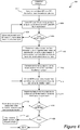
- FIG. 4 is a flowchart illustrating an inspection procedure 400 in accordance with one embodiment of the present invention.
- a BF is initially generated and directed towards a sample spot in operation 402.
- a DF illumination beam may also be directed towards such initial sample spot.
- a BF (and DF) output beam may then be detected from the sample spot in response to the BF (and DF) illumination beam in operation 404.
- BF and DF output data such as detected signals or images, may be simultaneously collected.
- the BF (and DF) beam may be scanned across individual swaths of the sample. For instance, the BF and DF beams are scanned across a first swath in a first scan direction. These BF and DF beams may then be scanned across another a second swath in a scan direction that is opposite to the first swath's scan direction so that a serpentine scan pattern is implemented. Alternatively, the BF and DF beams may be scanned across the sample with any suitable scan pattern, such as a circular or spiral scan pattern.
- the sensors may have to be arranged differently ( e . g ., in a circular pattern) and/or the sample may be moved differently ( e . g ., rotated) during scanning in order to scan a circular or spiral shape from the sample.
- surface or near-surface characteristics of the inspected area may then be determined based on the detected BF (and DF) output beam to find candidate locations that are likely to have additional defects below the surface in operation 410. That is, candidate locations that may contain defects that are not on the surface or near the surface may be located by analysis of the BF (and DF) output data.
- die-to-die, cell-to-cell, or die-to-database comparisons are performed to locate differences that are above a particular threshold, and these differences may then be classified as specific defect types. Some of these defect types may be determined to correlate with deeper defects.
- BF output data can generally be used to detect defects in the form of planar deformity of surface structures. For instance, some structures may appear larger or smaller than they are designed to be.
- the BF output data can also indicate changes in film thickness, for example, in the form of color changes. Color changes in the BF response can also be impacted by changes in the material itself ( e . g ., density changes). Additionally, groups of structures that have become defective (even if only individual structures within the group are defective) may affect the surrounding structures.
- DF output data can detect particle defects and roughness on the surface, local gradients in structure height for a particular structure, etc.
- Certain defect or sample characteristics types that are obtained from BF or DF output data may be used to find candidate locations for further MOR-based review. For instance, particular Cu-filled through Silicon via (TSV) or groups of TSV structures may have a difference in a particular defect type (e . g ., deformation) or characteristic (e.g., color), as compared to other TSV structures. These TSV's may be selected as candidate for further review by the MOR-based module.
- TSV Cu-filled through Silicon via
- the process is monitored using an averaging BF/DF technique to area anomalies. Averages in defect size, count, or other characteristics obtained from the BF/DF channels may be monitored per areas of the sample. For instance, a particular area may have bigger planar structures than other areas with the same type of structures, such as TSV's. Areas that deviate by a predetermined threshold from the average or mean of the other sample area may be selected as candidates for deeper MOR-based review. Alternatively, a sampling of locations within a deviating area may be selected for further MOR-based review. For instance, a particular large area having a plurality of TSV structures may be determined to have bigger structures, which may or not include TSV structures. A sampling of the TSV structures or all of the TSV structures within this particular large area may then be selected for MOR-based review. In one embodiment, candidate TSV locations are selected to be distributed across the particular area.
- a pump and probe beam (e.g., from the MOR-based module) may be generated and directed towards a first candidate location on the sample in operation 412.
- a MOR-based output beam from the candidate location may then be detected in response to the pump and probe illumination beam in operation 414.
- a modulated pump beam is directed to a pump spot at the first candidate location on the sample, and a probe beam is directed to at least a portion of such pump spot.
- the reflected signal from the probe beam is detected, for example, by a PT-detector as described above.
- a feature characteristic below the surface at the candidate location may be determined based on the MOR-based output beam in operation 415.
- the reflectivity data obtained from the MOR-based module can be used to find defects or further characterize features that are located deep in the sample at the candidate locations. Deeper defects and feature characteristics that can be monitored, measured, or found using a MOR-based review may include voids, particles, missing or added material, changes in sidewall angle, a sidewall's deviation from vertical, density changes in a material, etc.
- Training sets of known deep (or non-surface) characteristics and defects may be analyzed to determine their MOR-based output signal. Models may also be generated and trained to calculate particular characteristic values or defect types based on MOR-based reflectivity output data.
- the sample can be moved relative to the pump and probe illumination beam to scan a next candidate location in operation 418.
- the MOR-based channel is used to collect MOR-based output data for each candidate location until the last candidate is reviewed.
- the sample passes in operation 420 it may then be determined whether the sample passes in operation 420. For instance, it is determined whether the defects are yield-limiting defects or merely nuisance type defects.
- the BF, DF, and MOR-based defects and feature characteristics may all be analyzed to determine whether the sample passes. It may also be determined whether particular feature characteristics are out of specification. If the sample does not pass, the process may be altered; the sample may be repaired, or the sample may be discarded in operation 422. In one implementation, the sample is discarded and the process is altered. If the sample passes, the procedure 400 may end, and the sample may be used as a product or be further processed. After further processing, the sample may be again inspected.
- BF/DF channels in a first inspection pass can result in a more efficient inspection process.
- the BF/DF scans are significantly faster than a MOR-based scan. That is, the sample can be quickly scanned using a BF and/or DF inspection process. Suspect candidate locations can then be reviewed again by a MOR-based channel.
- the data that is obtained from the MOR-based review can be added to the data from the BF and/or DF inspection so as to provide a richer analysis for monitoring feature characteristics or finding defects on the sample.
- the MOR-based output data can be used to improve the sensitivity of the BF and DF output data.
- the thermal diffusion length in Copper can be varied significantly by adjusting the pump beam modulation frequency.
- the thermal diffusion length and the sensitivity region of the system can be as large as 50 - 100 um allowing characterization of deep voids in Cu TSV structures (40 - 60 um deep and 3-8 um wide).
- the BF modules can also be used to determine whether the TSVs have oxidized prior to inspection with a MOR-based module. For instance, a sampling of TSV images may be reviewed to determine whether there is oxide present. The presence of oxide during a MOR-based probe of TSV structures may cause the oxide to be burned off by the pump laser and cause unreliable results. It may be beneficial to remove the oxide from such TSV structures or the like. If there is oxide present, the sample may be polished (or some other technique implemented) so as to remove oxide. The MOR-based inspection can then proceed.
- the BF module may also be used to align the pump and probe beams with respect to a target structure.
- BF output data can be used to align the pump and probe beam so as to accurately probe one or more specific target locations of the target structure.
- the target structure is a TSV structure.
- Figure 5 is a flowchart illustrated a procedure 500 for aligning MOR-based illumination beams in accordance with a specific implementation of the present invention. Initially, a BF illumination beam may be generated and scanned over a target structure in operation 502. A BF output beam may then be detected from the target structure in response to the BF illumination beam in operation 504. In one example, an image of the target structure may be generated based on the BF output beam.
- the BF output beam may then be analyzed to determine one or more target locations on the scanned target structure in operation 506.
- the edges of the target may be determined, and the center of the target may then be determined for MOR-based probing.
- a line of pixels may be obtained across the width (or radius) of the target structure, and such line can be used to find the center of the target structure.
- two orthogonal directions of pixels may be obtained across the target structure to then locate a center of target structure.
- a number of target locations may be selected to be distributed across the target structure so as to substantially cover the area of the target structure.
- a particular pattern of target locations may be chosen for systematically probing the target structure.
- a spiral pattern of locations that spiral out from the center of the structure is selected.
- a grid of locations that can be scanned in a serpentine pattern across the target is selected.
- the TSV is probed so as to cover the entire TSV structure.
- a pump and probe beam may then be generated and directed towards a first target location on the sample in operation 508.
- a MOR-based output beam is then detected from the target location in response to the pump and probe illumination beam in operation 510. It may then be determined whether the last target location has been reached in operation 512. That is, it is determined whether the probe pattern is complete. If the last target location has not been reached, the sample may then be moved relative to the pump and probe illumination beam to scan the next target location in operation 514.
- a feature characteristic of the target structure that is below the surface may then be determined based on the MOR-based output beam in operation 516, as further described above.
- the alignment procedure 500 may be repeated on any number of target structures.
- inspection systems and techniques for characterizing deep defects or features are described herein as being applied to certain types of TSV structures, it is understood that embodiments of the present invention may be applied to any suitable 3D or vertical semiconductor structures, such as NAND or NOR memory devices formed using terabit cell array transistors (TCAT), vertical-stacked array transistors (VSAT), bit cost scalable technology (BiCST), piped shaped BiCS technology (P-BiCS), etc.
- TCAT terabit cell array transistors
- VSAT vertical-stacked array transistors
- BiCST bit cost scalable technology
- P-BiCS piped shaped BiCS technology
- the vertical direction is generally a direction that is perpendicular to the substrate surface.
- inspection embodiments may be applied at any point in the fabrication flow that results in multiple layers being formed on a substrate, and such layers may include any number and type of materials.
- the optical layout of the inspection/review tools can vary from that described above.
- the objective lens can be one of many possible layouts, as long as the transmission coatings are optimized for the particular selected wavelength band or sub-band and the aberration over each waveband is minimized.
- Any suitable lens arrangement may be used to direct each illumination beam towards the sample and direct the output beam emanating from the sample towards each detector.
- the illumination and collection optical elements of the system may be reflective or transmissive.
- the output beam may be reflected or scattered from the sample or transmitted through the sample.
Landscapes
- General Health & Medical Sciences (AREA)
- Health & Medical Sciences (AREA)
- Life Sciences & Earth Sciences (AREA)
- Chemical & Material Sciences (AREA)
- Analytical Chemistry (AREA)
- Biochemistry (AREA)
- Physics & Mathematics (AREA)
- General Physics & Mathematics (AREA)
- Immunology (AREA)
- Pathology (AREA)
- Investigating Materials By The Use Of Optical Means Adapted For Particular Applications (AREA)
- Testing Or Measuring Of Semiconductors Or The Like (AREA)
- Investigating Or Analyzing Materials Using Thermal Means (AREA)
Claims (11)
- Système de détection de défauts ou de vérification des défauts dans un échantillon de semi-conducteur (216), le système comprenant :un module de champ clair (BF) pour diriger un faisceau d'éclairage BF sur un spot BF sur un échantillon et détecter un faisceau de sortie réfléchie à partir du spot BF sur l'échantillon en réponse au faisceau d'éclairage BF dirigé sur le spot BF ;un module de réflexion optique modulée (MOR) pour diriger un faisceau de pompage sur un spot de pompage sur l'échantillon, diriger un faisceau de sonde vers un spot de sonde sur l'échantillon, et détecter un faisceau de sortie MOR à partir du spot de sonde en réponse au faisceau de pompage et au faisceau de sonde, dans lequel le spot de sonde coïncide avec le spot de pompage ;dans lequel le module MOR comprend :une source de laser à pompe (202c) pour générer le faisceau de pompage dans une plage de longueurs d'onde située entre environ 400 et 600 nm ;un modulateur (203) pour configurer la source de laser à pompe (202c) afin de moduler le faisceau de pompage ;une source de laser à onde continue (CW) de sonde (202d) pour générer le faisceau de sonde dans une plage de longueurs d'onde située entre environ 600 et 800 nm ;des optiques d'éclairage (210) pour diriger le faisceau de pompage et le faisceau de sonde vers l'échantillon ;des optiques de collecte pour diriger le faisceau de sortie MOR vers un détecteur photothermique (218d) ; etle détecteur photothermique (218d) pour détecter le faisceau de sortie MOR et générer un signal de sortie qui est filtré pour isoler les changements qui sont synchrones avec la modulation du faisceau de pompage ;un module de champ sombre (DF) pour diriger un faisceau d'éclairage DF sur un spot DF sur l'échantillon et détecter un faisceau de sortie diffusé à partir du spot DF sur l'échantillon en réponse au faisceau d'éclairage DF dirigé sur le spot DF ; dans lequel le module BF comporte une source de lumière BF (202a) pour générer le faisceau d'éclairage BF etle module DF comporte une source de lumière DF (202b) pour générer le faisceau d'éclairage DF ;
etun processeur (290) servant à exécuter ou à amener les opérations suivantes :le fait d'amener le module BF à balayer le faisceau d'éclairage BF sur une pluralité de spots BF sur l'échantillon et à détecter un faisceau de sortie à partir de la pluralité de spots BF ;le fait d'amener le module MOR à balayer le faisceau de pompage et de sonde sur une pluralité de spots de pompage et de sonde, respectivement, et à détecter un faisceau de sortie MOR à partir de la pluralité de spots de sonde ;l'analyse du faisceau de sortie BF provenant de la pluralité de spots BF pour détecter un ou plusieurs défauts sur une surface ou proches de la surface de l'échantillon ; etl'analyse du faisceau de sortie MOR provenant de la pluralité de spots de sonde pour détecter un ou plusieurs défauts se trouvant en dessous de la surface de l'échantillon. - Système selon la revendication 1, dans lequel le module BF et le module MOR partagent un objectif (210) ; ou
un même détecteur pour détecter le faisceau de sortie BF et le faisceau de sortie MOR. - Système selon la revendication 1, dans lequel le processeur (290) est configuré pour amener le faisceau d'éclairage BF et DF à balayer l'échantillon avant le balayage du faisceau de pompage et de sonde, dans lequel le processeur est configuré en outre pour déterminer un ou plusieurs emplacements cibles pour balayer le faisceau de pompage et de sonde sur la base de l'analyse du faisceau de sortie BF et DF après le balayage de la totalité de l'échantillon ou d'une partie de l'échantillon par le faisceau d'éclairage BF et DF ; ou
le module BF et DF partagent une source de lumière pour générer le faisceau d'éclairage BF et DF. - Système selon la revendication 1, dans lequel le module BF comprend :des optiques d'éclairage (210) pour diriger le faisceau d'éclairage BF vers l'échantillon ;des optiques de collecte pour diriger le faisceau de sortie BF vers un détecteur BF (218a) ;le détecteur BF (218a) pour détecter le faisceau de sortie BF ; et facultativement, les optiques d'éclairage du module BF partagent un ou plusieurs composants avec les optiques d'éclairage du module MOR, dans lequel les optiques de collecte du module BF partagent un ou plusieurs composants avec les optiques de collecte du module MOR.
- Système selon la revendication 1, dans lequel les un ou plusieurs défauts qui se trouvent en dessous de la surface comprennent un ou plusieurs vides ; ou
comprennent des changements de densité d'un matériau ou des changements d'angle de paroi latérale ; ou
sont présents à l'intérieur d'une ou de plusieurs structures d'interconnexion verticale (TSV). - Système selon la revendication 1, comprenant en outre un module de focalisation automatique (206) pour diriger un faisceau à focalisation automatique vers l'échantillon et détecter un faisceau réfléchi à partir de l'échantillon en réponse au faisceau à focalisation automatique, et ajuster un foyer du système, dans lequel le module BF, le module MOR, et le module de focalisation automatique partagent un objectif (210) .
- Système selon la revendication 1, dans lequel le processeur (290) est configuré pour amener le faisceau d'éclairage BF, la pompe, et le faisceau de sonde à balayer simultanément.
- Procédé de détection de défauts ou de vérification des défauts dans un échantillon de semi-conducteur, le procédé comprenant :le balayage d'une partie de l'échantillon avec un faisceau d'éclairage en champ clair (BF) ;la détection d'un faisceau de sortie BF réfléchi à partir de la partie d'échantillon quand le faisceau BF balaie la partie d'échantillon ;la détermination de caractéristiques de surface ou proches de la surface de la partie d'échantillon sur la base du faisceau de sortie BF détecté ;le fait de trouver des emplacements candidats à l'intérieur de la partie d'échantillon qui sont susceptibles de présenter des défauts supplémentaires en dessous d'une surface de l'échantillon sur la base des caractéristiques de surface ouproches de la surface déterminées de la partie d'échantillon qui ont été déterminées sur la base du faisceau de sortie BF détecté ;l'orientation d'un faisceau de pompage modulé et d'un faisceau de sonde sur chaque emplacement candidat ;la détection d'un signal de réflexion optique modulé à partir de chaque emplacement candidat en réponse à chaque faisceau de sonde dirigé vers chaque emplacement candidat ; etla détermination d'une caractéristique d'élément qui se trouve en dessous de la surface au niveau de chaque emplacement candidat sur la base du signal de réflexion optique modulé détecté à partir d'un tel emplacement candidat ;la détection d'un faisceau de sortie en champ sombre (DF) diffusé à partir de la partie d'échantillon quand le faisceau BF balaie la partie d'échantillon ou en réponse au balayage d'un faisceau en champ sombre sur la partie d'échantillon ;la détermination de caractéristiques de surface ou proches de la surface de la partie d'échantillon sur la base du faisceau de sortie DF détecté ; etle fait de trouver une seconde pluralité d'emplacements candidats sur la base des caractéristiques de surface ouproches de la surface de la partie d'échantillon sur la base du faisceau de sortie DF détecté ;la détection d'un signal de réflexion optique modulé à partir de chaque second emplacement candidat en réponse à chaque faisceau de sonde dirigé vers chaque second emplacement candidat ; etla détermination d'une caractéristique d'élément qui se trouve en dessous de la surface au niveau de chaque second emplacement candidat sur la base du signal de réflexion optique modulé détecté à partir d'un tel second emplacement candidat.
- Procédé selon la revendication 8, dans lequel les premiers et seconds emplacements candidats sont trouvés
par la mise en corrélation de caractéristiques de surface ou proches de la surface avec une présence de défauts de sub-surface ; ou
par la mise en corrélation de caractéristiques de surface ou proches de la surface avec une présence de défauts de sub-surface ; dans lequel les premiers et seconds emplacements candidats sont associés chacun à
une sous-zone de la partie d'échantillon qui présente une ou plusieurs caractéristiques de surface ou proches de la surface qui dévient d'une quantité prédéfinie par rapport à une moyenne de la partie d'échantillon ; ou une sous-zone de la partie d'échantillon qui présente une ou plusieurs caractéristiques de surface ou proches de la surface qui dévient d'une quantité prédéfinie par rapport à une moyenne de la partie d'échantillon ; dans lequel au moins un des premiers et seconds emplacements candidats comporte des interconnexions verticales (TSV) ; ou les premiers et seconds emplacements candidats sont sélectionnés de manière à être répartis à travers leur sous-zone associée. - Procédé selon la revendication 8, comprenant en outre :le fait de déterminer si les caractéristiques de surface ou proches de la surface indiquent une présence d'oxydation sur le substrat ; etl'élimination de l'oxydation avant de diriger le faisceau de pompage modulé et le faisceau de sonde au niveau de chaque emplacement candidat.
- Procédé selon la revendication 8, dans lequel au moins certains des emplacements candidats sont
sélectionnés chacun de manière à être centrés sur une structure sur la base d'une image d'une telle structure qui est générée sur la base du faisceau de sortie BF ; ou sélectionnés en outre de manière à être répartis à travers une structure sur la base d'une image d'une telle structure qui est générée sur la base du faisceau de sortie BF.
Applications Claiming Priority (3)
| Application Number | Priority Date | Filing Date | Title |
|---|---|---|---|
| US201461939135P | 2014-02-12 | 2014-02-12 | |
| US14/618,586 US9772297B2 (en) | 2014-02-12 | 2015-02-10 | Apparatus and methods for combined brightfield, darkfield, and photothermal inspection |
| PCT/US2015/015471 WO2015123337A1 (fr) | 2014-02-12 | 2015-02-11 | Appareil et procédés pour l'inspection combinée de fond clair, de fond noir et photothermique |
Publications (3)
| Publication Number | Publication Date |
|---|---|
| EP3100032A1 EP3100032A1 (fr) | 2016-12-07 |
| EP3100032A4 EP3100032A4 (fr) | 2017-08-30 |
| EP3100032B1 true EP3100032B1 (fr) | 2018-10-03 |
Family
ID=53774707
Family Applications (1)
| Application Number | Title | Priority Date | Filing Date |
|---|---|---|---|
| EP15749379.2A Active EP3100032B1 (fr) | 2014-02-12 | 2015-02-11 | Appareil et procédé pour l'inspection combinée en champ clair, en champ sombre et photothermique |
Country Status (7)
| Country | Link |
|---|---|
| US (2) | US9772297B2 (fr) |
| EP (1) | EP3100032B1 (fr) |
| JP (3) | JP6552513B2 (fr) |
| KR (1) | KR102155927B1 (fr) |
| CN (1) | CN106030292B (fr) |
| TW (1) | TWI657239B (fr) |
| WO (1) | WO2015123337A1 (fr) |
Families Citing this family (37)
| Publication number | Priority date | Publication date | Assignee | Title |
|---|---|---|---|---|
| US9772297B2 (en) | 2014-02-12 | 2017-09-26 | Kla-Tencor Corporation | Apparatus and methods for combined brightfield, darkfield, and photothermal inspection |
| DE102015202172B4 (de) * | 2015-02-06 | 2017-01-19 | Carl Zeiss Microscopy Gmbh | Teilchenstrahlsystem und Verfahren zur teilchenoptischen Untersuchung eines Objekts |
| US9772540B2 (en) * | 2015-07-09 | 2017-09-26 | Bio-Tek Instruments, Inc. | Autofocus for imaging system |
| JP6723633B2 (ja) * | 2015-12-10 | 2020-07-15 | 株式会社ディスコ | 検査装置 |
| CN109073565B (zh) * | 2016-02-03 | 2022-03-15 | 科磊股份有限公司 | 晶片缺陷检查及审查系统 |
| US10204416B2 (en) * | 2016-02-04 | 2019-02-12 | Kla-Tencor Corporation | Automatic deskew using design files or inspection images |
| CN109196336B (zh) * | 2016-06-02 | 2021-10-15 | 东京毅力科创株式会社 | 利用奇异光束的暗场晶片纳米缺陷检查系统 |
| WO2017222670A1 (fr) * | 2016-06-22 | 2017-12-28 | University Of Virginia Patent Foundation | Système de mesure de propriété de matériau à base de fibre optique et procédés associés |
| US11047806B2 (en) * | 2016-11-30 | 2021-06-29 | Kla-Tencor Corporation | Defect discovery and recipe optimization for inspection of three-dimensional semiconductor structures |
| US11397158B2 (en) | 2017-03-29 | 2022-07-26 | Agency For Science, Technology And Research | Reconfigurable laser stimulated lock-in thermography for micro-crack detection |
| CN107611046A (zh) * | 2017-07-28 | 2018-01-19 | 华灿光电(浙江)有限公司 | 一种内层缺陷的检测装置及检测方法 |
| CN109387518B (zh) | 2017-08-02 | 2022-06-17 | 上海微电子装备(集团)股份有限公司 | 自动光学检测方法 |
| CN108398404A (zh) * | 2018-02-05 | 2018-08-14 | 南京理工大学 | 基于激光散斑的闪点强弱检测装置及方法 |
| US10928311B2 (en) * | 2018-04-17 | 2021-02-23 | The Government Of The United States Of America, As Represented By The Secretary Of The Navy | Rapid multiplexed infrared 3D nano-tomography |
| US10295476B1 (en) * | 2018-08-14 | 2019-05-21 | Applied Materials Israel Ltd. | System and method for multiple mode inspection of a sample |
| JP7121606B2 (ja) * | 2018-09-11 | 2022-08-18 | 浜松ホトニクス株式会社 | 光計測装置 |
| US11320387B2 (en) | 2018-11-28 | 2022-05-03 | International Business Machines Corporation | Structure facilitating optically checking via formation |
| CN109444166B (zh) * | 2018-12-04 | 2021-07-23 | 电子科技大学 | 一种大口径光学元件表面吸收型缺陷分布快速成像的方法 |
| KR102597603B1 (ko) * | 2018-12-10 | 2023-11-02 | 삼성전자주식회사 | 검사 장치 및 이를 포함하는 반도체 구조 제조 장치 |
| CN111380874B (zh) * | 2018-12-28 | 2021-04-30 | 上海微电子装备(集团)股份有限公司 | 缺陷检测装置、键合设备以及键合方法 |
| US11137350B2 (en) * | 2019-01-28 | 2021-10-05 | Kla Corporation | Mid-infrared spectroscopy for measurement of high aspect ratio structures |
| WO2020237198A1 (fr) * | 2019-05-23 | 2020-11-26 | Onto Innovation Inc. | Systèmes et procédés de métrologie de fabrication et de controle non destructifs |
| CN110346381B (zh) * | 2019-08-12 | 2022-03-08 | 衡阳师范学院 | 一种光学元件损伤测试方法及装置 |
| KR102229881B1 (ko) * | 2019-09-27 | 2021-03-19 | 한국기초과학지원연구원 | 광열반사 스펙트럼 측정장치 및 이의 동작 방법 |
| FR3102849B1 (fr) | 2019-11-04 | 2022-02-11 | Office National Detudes Rech Aerospatiales | Analyse photothermique d’une piece de materiau solide |
| JP7483893B2 (ja) * | 2019-12-31 | 2024-05-15 | エーエスエムエル ホールディング エヌ.ブイ. | 汚染検出計測システム、リソグラフィ装置、それらの方法 |
| JP7428616B2 (ja) * | 2020-08-27 | 2024-02-06 | 株式会社日立パワーソリューションズ | 超音波検査装置及び超音波検査方法 |
| CN114486901A (zh) * | 2020-11-13 | 2022-05-13 | 深圳中科飞测科技股份有限公司 | 承载组件及检测设备 |
| CN113049599B (zh) * | 2021-03-25 | 2024-10-25 | 深圳中科飞测科技股份有限公司 | 调节方法及装置、检测设备、可读存储介质及检测系统 |
| CN114881990B (zh) * | 2022-05-23 | 2025-10-31 | 北京御微半导体技术有限公司 | 掩模版缺陷检测方法、装置、电子设备及存储介质 |
| WO2024003850A1 (fr) * | 2022-06-30 | 2024-01-04 | Nova Ltd. | Évaluation des anomalies d'un échantillon |
| EP4573356A1 (fr) * | 2022-08-15 | 2025-06-25 | Trustees of Boston University | Système de microscopie photothermique à infrarouge moyen à débit vidéo utilisant un balayage laser synchronisé |
| US12405215B2 (en) * | 2023-04-14 | 2025-09-02 | Photothermal Spectroscopy Corp. | Asymmetric quadrature interferometry for thin film interference suppression in optical photothermal infrared spectroscopy |
| KR102830664B1 (ko) * | 2023-11-08 | 2025-07-07 | (주)뮤텍코리아 | 반도체 웨이퍼의 나노급 파티클 검사를 위한 광학 시스템 |
| CN119915819B (zh) * | 2024-12-12 | 2025-12-26 | 上海中科飞测半导体科技有限公司 | 一种光学检测设备及其控制方法 |
| CN120314303B (zh) * | 2025-03-13 | 2025-12-23 | 飞测思凯浦(上海)半导体科技有限公司 | 一种成像调节装置和光学检测设备 |
| CN119985535A (zh) * | 2025-04-14 | 2025-05-13 | 清软微视(杭州)科技有限公司 | 一种多通道同时扫描的晶圆检测系统 |
Family Cites Families (65)
| Publication number | Priority date | Publication date | Assignee | Title |
|---|---|---|---|---|
| DE3037983C2 (de) | 1980-10-08 | 1983-03-31 | Fa. Carl Zeiss, 7920 Heidenheim | Verfahren und Vorrichtung zur lichtinduzierten rastermikroskopischen Darstellung von Probenparametern in ihrer räumlichen Verteilung |
| US4750822A (en) | 1986-03-28 | 1988-06-14 | Therma-Wave, Inc. | Method and apparatus for optically detecting surface states in materials |
| US4795260A (en) * | 1987-05-15 | 1989-01-03 | Therma-Wave, Inc. | Apparatus for locating and testing areas of interest on a workpiece |
| US5058982A (en) | 1989-06-21 | 1991-10-22 | Orbot Systems Ltd. | Illumination system and inspection apparatus including same |
| JPH0349296A (ja) * | 1989-07-18 | 1991-03-04 | Fujitsu Ltd | バイアホール検査装置 |
| JPH03179243A (ja) * | 1989-12-07 | 1991-08-05 | Fujitsu Ltd | スルーホール充填状態検査装置 |
| US5074669A (en) | 1989-12-12 | 1991-12-24 | Therma-Wave, Inc. | Method and apparatus for evaluating ion implant dosage levels in semiconductors |
| US5781294A (en) | 1991-12-24 | 1998-07-14 | Hitachi, Ltd. | Method and apparatus for detecting photoacoustic signal to detect surface and subsurface information of the specimen |
| US5248876A (en) | 1992-04-21 | 1993-09-28 | International Business Machines Corporation | Tandem linear scanning confocal imaging system with focal volumes at different heights |
| JPH07231023A (ja) * | 1994-02-17 | 1995-08-29 | Fujitsu Ltd | 薄膜の形状計測方法 |
| JP2682461B2 (ja) * | 1994-08-29 | 1997-11-26 | 日本電気株式会社 | 構造欠陥検査装置 |
| US20020054291A1 (en) | 1997-06-27 | 2002-05-09 | Tsai Bin-Ming Benjamin | Inspection system simultaneously utilizing monochromatic darkfield and broadband brightfield illumination sources |
| US6288780B1 (en) | 1995-06-06 | 2001-09-11 | Kla-Tencor Technologies Corp. | High throughput brightfield/darkfield wafer inspection system using advanced optical techniques |
| DE19713362A1 (de) | 1997-03-29 | 1998-10-01 | Zeiss Carl Jena Gmbh | Konfokale mikroskopische Anordnung |
| DE19714221A1 (de) | 1997-04-07 | 1998-10-08 | Zeiss Carl Fa | Konfokales Mikroskop mit einem motorischen Scanningtisch |
| JPH1114575A (ja) * | 1997-06-24 | 1999-01-22 | Osaka Sangyo Univ | 光熱反射型試料分析装置 |
| EP0930498A3 (fr) * | 1997-12-26 | 1999-11-17 | Nidek Co., Ltd. | Dispositif de contrÔle et procédé de détection de défauts |
| US6552803B1 (en) | 1998-02-24 | 2003-04-22 | Kla-Tencor Corporation | Detection of film thickness through induced acoustic pulse-echos |
| JPH11304740A (ja) * | 1998-04-20 | 1999-11-05 | Matsushita Electric Ind Co Ltd | 導電性ペースト充填状態検査方法 |
| US6248988B1 (en) | 1998-05-05 | 2001-06-19 | Kla-Tencor Corporation | Conventional and confocal multi-spot scanning optical microscope |
| US6054868A (en) * | 1998-06-10 | 2000-04-25 | Boxer Cross Incorporated | Apparatus and method for measuring a property of a layer in a multilayered structure |
| US6867406B1 (en) | 1999-03-23 | 2005-03-15 | Kla-Tencor Corporation | Confocal wafer inspection method and apparatus using fly lens arrangement |
| US6268916B1 (en) * | 1999-05-11 | 2001-07-31 | Kla-Tencor Corporation | System for non-destructive measurement of samples |
| US6535285B1 (en) | 2000-02-08 | 2003-03-18 | Therma-Wave, Inc. | Combination thermal wave and optical spectroscopy measurement system |
| JP3671822B2 (ja) * | 2000-07-26 | 2005-07-13 | 株式会社日立製作所 | 欠陥検査方法および欠陥検査システム |
| US6891627B1 (en) | 2000-09-20 | 2005-05-10 | Kla-Tencor Technologies Corp. | Methods and systems for determining a critical dimension and overlay of a specimen |
| IL146174A (en) | 2001-10-25 | 2007-08-19 | Camtek Ltd | Confocal system for testing woofers |
| US6654109B2 (en) | 2002-02-05 | 2003-11-25 | Taiwan Semiconductor Manufacturing Co. Ltd | System for detecting surface defects in semiconductor wafers |
| US7027142B2 (en) * | 2002-05-06 | 2006-04-11 | Applied Materials, Israel, Ltd. | Optical technique for detecting buried defects in opaque films |
| US20040075879A1 (en) | 2002-05-29 | 2004-04-22 | Accretech (Israel) Ltd. | Multiple scanning system and method |
| US7106446B2 (en) | 2002-06-21 | 2006-09-12 | Therma-Wave, Inc. | Modulated reflectance measurement system with multiple wavelengths |
| US7079249B2 (en) * | 2002-06-21 | 2006-07-18 | Therma-Wave, Inc. | Modulated reflectance measurement system with fiber laser technology |
| US20040051976A1 (en) | 2002-08-29 | 2004-03-18 | Accretech (Israel) Ltd | Confocal microscope with diffractively formed virtual pinhole array |
| US6963393B2 (en) * | 2002-09-23 | 2005-11-08 | Applied Materials, Inc. | Measurement of lateral diffusion of diffused layers |
| US20040140417A1 (en) | 2002-12-27 | 2004-07-22 | Accretech (Israel) Ltd. | Image sensor for confocal microscopy |
| US7075058B2 (en) | 2003-03-28 | 2006-07-11 | The United States Of America As Represented By The United States Department Of Energy | Photothermal imaging scanning microscopy |
| US7212288B2 (en) | 2003-08-14 | 2007-05-01 | Therma-Wave, Inc. | Position modulated optical reflectance measurement system for semiconductor metrology |
| US7288366B2 (en) | 2003-10-24 | 2007-10-30 | Chartered Semiconductor Manufacturing Ltd. | Method for dual damascene patterning with single exposure using tri-tone phase shift mask |
| US20050111082A1 (en) | 2003-11-20 | 2005-05-26 | Accretech (Israel) Ltd. | Confocal microscopy arrangement without beam splitter |
| DE102004004761A1 (de) | 2004-01-30 | 2005-09-08 | Leica Microsystems Semiconductor Gmbh | Vorrichtung und Verfahren zur Inspektion eines Wafers |
| US7026175B2 (en) | 2004-03-29 | 2006-04-11 | Applied Materials, Inc. | High throughput measurement of via defects in interconnects |
| US7259869B2 (en) | 2004-06-29 | 2007-08-21 | Kla-Tencor Technologies Corporation | System and method for performing bright field and dark field optical inspection |
| WO2006006148A2 (fr) | 2004-07-12 | 2006-01-19 | Negevtech Ltd. | Procede et appareil d'inspection multimode |
| JP2006308513A (ja) * | 2005-05-02 | 2006-11-09 | Nec Electronics Corp | 検査装置及び方法 |
| JP4713217B2 (ja) * | 2005-05-13 | 2011-06-29 | ルネサスエレクトロニクス株式会社 | 検査装置及び方法 |
| TWM279563U (en) * | 2005-05-20 | 2005-11-01 | Huang-Guo Liau | Caster structure for infant stroller |
| JP2007071803A (ja) * | 2005-09-09 | 2007-03-22 | Hitachi High-Technologies Corp | 欠陥観察方法及びその装置 |
| JP4723362B2 (ja) | 2005-11-29 | 2011-07-13 | 株式会社日立ハイテクノロジーズ | 光学式検査装置及びその方法 |
| US7724362B1 (en) | 2006-03-14 | 2010-05-25 | Kla-Tencor Corporation | Oblique incidence macro wafer inspection |
| JP2007294604A (ja) * | 2006-04-24 | 2007-11-08 | Tokyo Seimitsu Co Ltd | 外観検査装置及び外観検査方法 |
| US7502104B2 (en) | 2006-08-10 | 2009-03-10 | Kla-Tencor Corporation | Probe beam profile modulated optical reflectance system and methods |
| US7714999B2 (en) * | 2006-12-06 | 2010-05-11 | Applied Materials Israel, Ltd. | High resolution wafer inspection system |
| US7705977B2 (en) | 2006-12-21 | 2010-04-27 | Kla-Tencor Corporation | Methods for depth profiling in semiconductors using modulated optical reflectance technology |
| JP5055385B2 (ja) | 2007-02-28 | 2012-10-24 | ルドルフテクノロジーズ インコーポレイテッド | エロージョンにさらされる可能性のある試料の金属部分のピコ秒超音波を用いた特性化 |
| US7782452B2 (en) | 2007-08-31 | 2010-08-24 | Kla-Tencor Technologies Corp. | Systems and method for simultaneously inspecting a specimen with two distinct channels |
| US7755752B1 (en) * | 2008-04-07 | 2010-07-13 | Kla-Tencor Corporation | Combined modulated optical reflectance and photoreflectance system |
| US8203120B2 (en) | 2008-10-09 | 2012-06-19 | California Institute Of Technology | 4D imaging in an ultrafast electron microscope |
| SG164293A1 (en) | 2009-01-13 | 2010-09-29 | Semiconductor Technologies & Instruments Pte | System and method for inspecting a wafer |
| DE102009044151B4 (de) | 2009-05-19 | 2012-03-29 | Kla-Tencor Mie Gmbh | Vorrichtung zur optischen Waferinspektion |
| US8111399B2 (en) | 2009-06-30 | 2012-02-07 | Kla-Tencor Corporation | System and method for performing photothermal measurements and relaxation compensation |
| SG177786A1 (en) | 2010-07-13 | 2012-02-28 | Semiconductor Tech & Instr Inc | System and method for capturing illumination reflected in multiple directions |
| TWI503520B (zh) | 2011-01-19 | 2015-10-11 | 諾發測量儀器股份有限公司 | 光學系統及在三維構造中之量測方法 |
| IL213025A0 (en) | 2011-05-19 | 2011-07-31 | May High Tech Solution Ltd | Method and apparatus for optical inspection, detection and analysis of double sided and wafer edge macro defects |
| JP5889699B2 (ja) * | 2012-03-30 | 2016-03-22 | 株式会社日立ハイテクノロジーズ | 磁気メディアの光学式検査方法及びその装置 |
| US9772297B2 (en) | 2014-02-12 | 2017-09-26 | Kla-Tencor Corporation | Apparatus and methods for combined brightfield, darkfield, and photothermal inspection |
-
2015
- 2015-02-10 US US14/618,586 patent/US9772297B2/en active Active
- 2015-02-11 WO PCT/US2015/015471 patent/WO2015123337A1/fr not_active Ceased
- 2015-02-11 EP EP15749379.2A patent/EP3100032B1/fr active Active
- 2015-02-11 JP JP2016551771A patent/JP6552513B2/ja active Active
- 2015-02-11 KR KR1020167024932A patent/KR102155927B1/ko active Active
- 2015-02-11 CN CN201580008360.9A patent/CN106030292B/zh active Active
- 2015-02-12 TW TW104104820A patent/TWI657239B/zh active
-
2017
- 2017-08-31 US US15/692,863 patent/US10533954B2/en active Active
-
2019
- 2019-07-03 JP JP2019124766A patent/JP2019200212A/ja active Pending
-
2022
- 2022-05-26 JP JP2022085749A patent/JP7561793B2/ja active Active
Non-Patent Citations (1)
| Title |
|---|
| None * |
Also Published As
| Publication number | Publication date |
|---|---|
| US10533954B2 (en) | 2020-01-14 |
| TW201534902A (zh) | 2015-09-16 |
| JP2022119894A (ja) | 2022-08-17 |
| CN106030292A (zh) | 2016-10-12 |
| JP7561793B2 (ja) | 2024-10-04 |
| US9772297B2 (en) | 2017-09-26 |
| US20180003648A1 (en) | 2018-01-04 |
| EP3100032A4 (fr) | 2017-08-30 |
| US20150226676A1 (en) | 2015-08-13 |
| WO2015123337A1 (fr) | 2015-08-20 |
| TWI657239B (zh) | 2019-04-21 |
| KR20160123337A (ko) | 2016-10-25 |
| JP2019200212A (ja) | 2019-11-21 |
| JP6552513B2 (ja) | 2019-07-31 |
| JP2017511880A (ja) | 2017-04-27 |
| EP3100032A1 (fr) | 2016-12-07 |
| CN106030292B (zh) | 2020-03-27 |
| KR102155927B1 (ko) | 2020-09-14 |
Similar Documents
| Publication | Publication Date | Title |
|---|---|---|
| JP7561793B2 (ja) | 半導体試料内の瑕疵を検出又は精査するシステム | |
| JP5032114B2 (ja) | パターン化ウェハまたは非パターン化ウェハおよびその他の検体の検査システム | |
| KR102235580B1 (ko) | 반도체 웨이퍼 검사를 위한 결함 마킹 | |
| CN107003250B (zh) | 检验系统及具有增强检测的技术 | |
| US6842259B2 (en) | Analysis of isolated and aperiodic structures with simultaneous multiple angle of incidence measurements | |
| US8885037B2 (en) | Defect inspection method and apparatus therefor | |
| JP5221858B2 (ja) | 欠陥検査装置、及び欠陥検査方法 | |
| US9019492B2 (en) | Defect inspection device and defect inspection method | |
| JP5712079B2 (ja) | 欠陥検査装置および欠陥検査方法 | |
| KR20190082911A (ko) | 3차원 반도체 구조체들의 검사를 위한 결함 발견 및 레시피 최적화 | |
| WO2010024324A1 (fr) | Dispositif d'inspection de semi-conducteurs et procédé d'inspection | |
| JP2021527813A (ja) | 多重散乱信号に基づく埋設粒子深度値域分類 |
Legal Events
| Date | Code | Title | Description |
|---|---|---|---|
| PUAI | Public reference made under article 153(3) epc to a published international application that has entered the european phase |
Free format text: ORIGINAL CODE: 0009012 |
|
| STAA | Information on the status of an ep patent application or granted ep patent |
Free format text: STATUS: REQUEST FOR EXAMINATION WAS MADE |
|
| 17P | Request for examination filed |
Effective date: 20160720 |
|
| AK | Designated contracting states |
Kind code of ref document: A1 Designated state(s): AL AT BE BG CH CY CZ DE DK EE ES FI FR GB GR HR HU IE IS IT LI LT LU LV MC MK MT NL NO PL PT RO RS SE SI SK SM TR |
|
| AX | Request for extension of the european patent |
Extension state: BA ME |
|
| DAX | Request for extension of the european patent (deleted) | ||
| A4 | Supplementary search report drawn up and despatched |
Effective date: 20170801 |
|
| RIC1 | Information provided on ipc code assigned before grant |
Ipc: G01N 21/39 20060101ALI20170726BHEP Ipc: H01L 21/66 20060101ALI20170726BHEP Ipc: G01N 21/88 20060101ALI20170726BHEP Ipc: G01N 21/95 20060101AFI20170726BHEP Ipc: G01N 21/17 20060101ALI20170726BHEP |
|
| GRAP | Despatch of communication of intention to grant a patent |
Free format text: ORIGINAL CODE: EPIDOSNIGR1 |
|
| STAA | Information on the status of an ep patent application or granted ep patent |
Free format text: STATUS: GRANT OF PATENT IS INTENDED |
|
| INTG | Intention to grant announced |
Effective date: 20180420 |
|
| GRAS | Grant fee paid |
Free format text: ORIGINAL CODE: EPIDOSNIGR3 |
|
| GRAA | (expected) grant |
Free format text: ORIGINAL CODE: 0009210 |
|
| STAA | Information on the status of an ep patent application or granted ep patent |
Free format text: STATUS: THE PATENT HAS BEEN GRANTED |
|
| AK | Designated contracting states |
Kind code of ref document: B1 Designated state(s): AL AT BE BG CH CY CZ DE DK EE ES FI FR GB GR HR HU IE IS IT LI LT LU LV MC MK MT NL NO PL PT RO RS SE SI SK SM TR |
|
| REG | Reference to a national code |
Ref country code: GB Ref legal event code: FG4D |
|
| REG | Reference to a national code |
Ref country code: CH Ref legal event code: EP Ref country code: AT Ref legal event code: REF Ref document number: 1049135 Country of ref document: AT Kind code of ref document: T Effective date: 20181015 |
|
| REG | Reference to a national code |
Ref country code: NL Ref legal event code: FP |
|
| REG | Reference to a national code |
Ref country code: IE Ref legal event code: FG4D Ref country code: DE Ref legal event code: R096 Ref document number: 602015017524 Country of ref document: DE |
|
| REG | Reference to a national code |
Ref country code: LT Ref legal event code: MG4D |
|
| REG | Reference to a national code |
Ref country code: AT Ref legal event code: MK05 Ref document number: 1049135 Country of ref document: AT Kind code of ref document: T Effective date: 20181003 |
|
| PG25 | Lapsed in a contracting state [announced via postgrant information from national office to epo] |
Ref country code: LV Free format text: LAPSE BECAUSE OF FAILURE TO SUBMIT A TRANSLATION OF THE DESCRIPTION OR TO PAY THE FEE WITHIN THE PRESCRIBED TIME-LIMIT Effective date: 20181003 Ref country code: AT Free format text: LAPSE BECAUSE OF FAILURE TO SUBMIT A TRANSLATION OF THE DESCRIPTION OR TO PAY THE FEE WITHIN THE PRESCRIBED TIME-LIMIT Effective date: 20181003 Ref country code: NO Free format text: LAPSE BECAUSE OF FAILURE TO SUBMIT A TRANSLATION OF THE DESCRIPTION OR TO PAY THE FEE WITHIN THE PRESCRIBED TIME-LIMIT Effective date: 20190103 Ref country code: LT Free format text: LAPSE BECAUSE OF FAILURE TO SUBMIT A TRANSLATION OF THE DESCRIPTION OR TO PAY THE FEE WITHIN THE PRESCRIBED TIME-LIMIT Effective date: 20181003 Ref country code: ES Free format text: LAPSE BECAUSE OF FAILURE TO SUBMIT A TRANSLATION OF THE DESCRIPTION OR TO PAY THE FEE WITHIN THE PRESCRIBED TIME-LIMIT Effective date: 20181003 Ref country code: HR Free format text: LAPSE BECAUSE OF FAILURE TO SUBMIT A TRANSLATION OF THE DESCRIPTION OR TO PAY THE FEE WITHIN THE PRESCRIBED TIME-LIMIT Effective date: 20181003 Ref country code: PL Free format text: LAPSE BECAUSE OF FAILURE TO SUBMIT A TRANSLATION OF THE DESCRIPTION OR TO PAY THE FEE WITHIN THE PRESCRIBED TIME-LIMIT Effective date: 20181003 Ref country code: BG Free format text: LAPSE BECAUSE OF FAILURE TO SUBMIT A TRANSLATION OF THE DESCRIPTION OR TO PAY THE FEE WITHIN THE PRESCRIBED TIME-LIMIT Effective date: 20190103 Ref country code: FI Free format text: LAPSE BECAUSE OF FAILURE TO SUBMIT A TRANSLATION OF THE DESCRIPTION OR TO PAY THE FEE WITHIN THE PRESCRIBED TIME-LIMIT Effective date: 20181003 Ref country code: CZ Free format text: LAPSE BECAUSE OF FAILURE TO SUBMIT A TRANSLATION OF THE DESCRIPTION OR TO PAY THE FEE WITHIN THE PRESCRIBED TIME-LIMIT Effective date: 20181003 Ref country code: IS Free format text: LAPSE BECAUSE OF FAILURE TO SUBMIT A TRANSLATION OF THE DESCRIPTION OR TO PAY THE FEE WITHIN THE PRESCRIBED TIME-LIMIT Effective date: 20190203 |
|
| PG25 | Lapsed in a contracting state [announced via postgrant information from national office to epo] |
Ref country code: GR Free format text: LAPSE BECAUSE OF FAILURE TO SUBMIT A TRANSLATION OF THE DESCRIPTION OR TO PAY THE FEE WITHIN THE PRESCRIBED TIME-LIMIT Effective date: 20190104 Ref country code: SE Free format text: LAPSE BECAUSE OF FAILURE TO SUBMIT A TRANSLATION OF THE DESCRIPTION OR TO PAY THE FEE WITHIN THE PRESCRIBED TIME-LIMIT Effective date: 20181003 Ref country code: RS Free format text: LAPSE BECAUSE OF FAILURE TO SUBMIT A TRANSLATION OF THE DESCRIPTION OR TO PAY THE FEE WITHIN THE PRESCRIBED TIME-LIMIT Effective date: 20181003 Ref country code: PT Free format text: LAPSE BECAUSE OF FAILURE TO SUBMIT A TRANSLATION OF THE DESCRIPTION OR TO PAY THE FEE WITHIN THE PRESCRIBED TIME-LIMIT Effective date: 20190203 Ref country code: AL Free format text: LAPSE BECAUSE OF FAILURE TO SUBMIT A TRANSLATION OF THE DESCRIPTION OR TO PAY THE FEE WITHIN THE PRESCRIBED TIME-LIMIT Effective date: 20181003 |
|
| REG | Reference to a national code |
Ref country code: DE Ref legal event code: R097 Ref document number: 602015017524 Country of ref document: DE |
|
| PG25 | Lapsed in a contracting state [announced via postgrant information from national office to epo] |
Ref country code: DK Free format text: LAPSE BECAUSE OF FAILURE TO SUBMIT A TRANSLATION OF THE DESCRIPTION OR TO PAY THE FEE WITHIN THE PRESCRIBED TIME-LIMIT Effective date: 20181003 Ref country code: IT Free format text: LAPSE BECAUSE OF FAILURE TO SUBMIT A TRANSLATION OF THE DESCRIPTION OR TO PAY THE FEE WITHIN THE PRESCRIBED TIME-LIMIT Effective date: 20181003 |
|
| PLBE | No opposition filed within time limit |
Free format text: ORIGINAL CODE: 0009261 |
|
| STAA | Information on the status of an ep patent application or granted ep patent |
Free format text: STATUS: NO OPPOSITION FILED WITHIN TIME LIMIT |
|
| PG25 | Lapsed in a contracting state [announced via postgrant information from national office to epo] |
Ref country code: RO Free format text: LAPSE BECAUSE OF FAILURE TO SUBMIT A TRANSLATION OF THE DESCRIPTION OR TO PAY THE FEE WITHIN THE PRESCRIBED TIME-LIMIT Effective date: 20181003 Ref country code: SK Free format text: LAPSE BECAUSE OF FAILURE TO SUBMIT A TRANSLATION OF THE DESCRIPTION OR TO PAY THE FEE WITHIN THE PRESCRIBED TIME-LIMIT Effective date: 20181003 Ref country code: SM Free format text: LAPSE BECAUSE OF FAILURE TO SUBMIT A TRANSLATION OF THE DESCRIPTION OR TO PAY THE FEE WITHIN THE PRESCRIBED TIME-LIMIT Effective date: 20181003 Ref country code: EE Free format text: LAPSE BECAUSE OF FAILURE TO SUBMIT A TRANSLATION OF THE DESCRIPTION OR TO PAY THE FEE WITHIN THE PRESCRIBED TIME-LIMIT Effective date: 20181003 |
|
| REG | Reference to a national code |
Ref country code: DE Ref legal event code: R119 Ref document number: 602015017524 Country of ref document: DE |
|
| 26N | No opposition filed |
Effective date: 20190704 |
|
| REG | Reference to a national code |
Ref country code: CH Ref legal event code: PL |
|
| GBPC | Gb: european patent ceased through non-payment of renewal fee |
Effective date: 20190211 |
|
| PG25 | Lapsed in a contracting state [announced via postgrant information from national office to epo] |
Ref country code: SI Free format text: LAPSE BECAUSE OF FAILURE TO SUBMIT A TRANSLATION OF THE DESCRIPTION OR TO PAY THE FEE WITHIN THE PRESCRIBED TIME-LIMIT Effective date: 20181003 Ref country code: LU Free format text: LAPSE BECAUSE OF NON-PAYMENT OF DUE FEES Effective date: 20190211 Ref country code: MC Free format text: LAPSE BECAUSE OF FAILURE TO SUBMIT A TRANSLATION OF THE DESCRIPTION OR TO PAY THE FEE WITHIN THE PRESCRIBED TIME-LIMIT Effective date: 20181003 |
|
| REG | Reference to a national code |
Ref country code: IE Ref legal event code: MM4A |
|
| PG25 | Lapsed in a contracting state [announced via postgrant information from national office to epo] |
Ref country code: LI Free format text: LAPSE BECAUSE OF NON-PAYMENT OF DUE FEES Effective date: 20190228 Ref country code: CH Free format text: LAPSE BECAUSE OF NON-PAYMENT OF DUE FEES Effective date: 20190228 |
|
| PG25 | Lapsed in a contracting state [announced via postgrant information from national office to epo] |
Ref country code: GB Free format text: LAPSE BECAUSE OF NON-PAYMENT OF DUE FEES Effective date: 20190211 Ref country code: DE Free format text: LAPSE BECAUSE OF NON-PAYMENT OF DUE FEES Effective date: 20190903 Ref country code: IE Free format text: LAPSE BECAUSE OF NON-PAYMENT OF DUE FEES Effective date: 20190211 |
|
| PG25 | Lapsed in a contracting state [announced via postgrant information from national office to epo] |
Ref country code: TR Free format text: LAPSE BECAUSE OF FAILURE TO SUBMIT A TRANSLATION OF THE DESCRIPTION OR TO PAY THE FEE WITHIN THE PRESCRIBED TIME-LIMIT Effective date: 20181003 |
|
| PG25 | Lapsed in a contracting state [announced via postgrant information from national office to epo] |
Ref country code: MT Free format text: LAPSE BECAUSE OF NON-PAYMENT OF DUE FEES Effective date: 20190211 |
|
| PG25 | Lapsed in a contracting state [announced via postgrant information from national office to epo] |
Ref country code: CY Free format text: LAPSE BECAUSE OF FAILURE TO SUBMIT A TRANSLATION OF THE DESCRIPTION OR TO PAY THE FEE WITHIN THE PRESCRIBED TIME-LIMIT Effective date: 20181003 |
|
| PG25 | Lapsed in a contracting state [announced via postgrant information from national office to epo] |
Ref country code: HU Free format text: LAPSE BECAUSE OF FAILURE TO SUBMIT A TRANSLATION OF THE DESCRIPTION OR TO PAY THE FEE WITHIN THE PRESCRIBED TIME-LIMIT; INVALID AB INITIO Effective date: 20150211 |
|
| PG25 | Lapsed in a contracting state [announced via postgrant information from national office to epo] |
Ref country code: MK Free format text: LAPSE BECAUSE OF FAILURE TO SUBMIT A TRANSLATION OF THE DESCRIPTION OR TO PAY THE FEE WITHIN THE PRESCRIBED TIME-LIMIT Effective date: 20181003 |
|
| P01 | Opt-out of the competence of the unified patent court (upc) registered |
Effective date: 20230525 |
|
| PGFP | Annual fee paid to national office [announced via postgrant information from national office to epo] |
Ref country code: NL Payment date: 20260226 Year of fee payment: 12 |
|
| PGFP | Annual fee paid to national office [announced via postgrant information from national office to epo] |
Ref country code: BE Payment date: 20260227 Year of fee payment: 12 |
|
| PGFP | Annual fee paid to national office [announced via postgrant information from national office to epo] |
Ref country code: FR Payment date: 20260225 Year of fee payment: 12 |