EP3100361B1 - Distribution d'horloge en mode courant - Google Patents
Distribution d'horloge en mode courant Download PDFInfo
- Publication number
- EP3100361B1 EP3100361B1 EP15743426.7A EP15743426A EP3100361B1 EP 3100361 B1 EP3100361 B1 EP 3100361B1 EP 15743426 A EP15743426 A EP 15743426A EP 3100361 B1 EP3100361 B1 EP 3100361B1
- Authority
- EP
- European Patent Office
- Prior art keywords
- current
- clock
- voltage
- integrated circuit
- large scale
- Prior art date
- Legal status (The legal status is an assumption and is not a legal conclusion. Google has not performed a legal analysis and makes no representation as to the accuracy of the status listed.)
- Active
Links
Images


Classifications
-
- H—ELECTRICITY
- H03—ELECTRONIC CIRCUITRY
- H03K—PULSE TECHNIQUE
- H03K3/00—Circuits for generating electric pulses; Monostable, bistable or multistable circuits
- H03K3/02—Generators characterised by the type of circuit or by the means used for producing pulses
- H03K3/353—Generators characterised by the type of circuit or by the means used for producing pulses by the use, as active elements, of field-effect transistors with internal or external positive feedback
- H03K3/356—Bistable circuits
- H03K3/356104—Bistable circuits using complementary field-effect transistors
-
- G—PHYSICS
- G06—COMPUTING OR CALCULATING; COUNTING
- G06F—ELECTRIC DIGITAL DATA PROCESSING
- G06F1/00—Details not covered by groups G06F3/00 - G06F13/00 and G06F21/00
- G06F1/04—Generating or distributing clock signals or signals derived directly therefrom
- G06F1/10—Distribution of clock signals, e.g. skew
-
- G—PHYSICS
- G05—CONTROLLING; REGULATING
- G05F—SYSTEMS FOR REGULATING ELECTRIC OR MAGNETIC VARIABLES
- G05F3/00—Non-retroactive systems for regulating electric variables by using an uncontrolled element, or an uncontrolled combination of elements, such element or such combination having self-regulating properties
- G05F3/02—Regulating voltage or current
- G05F3/08—Regulating voltage or current wherein the variable is DC
- G05F3/10—Regulating voltage or current wherein the variable is DC using uncontrolled devices with non-linear characteristics
- G05F3/16—Regulating voltage or current wherein the variable is DC using uncontrolled devices with non-linear characteristics being semiconductor devices
- G05F3/20—Regulating voltage or current wherein the variable is DC using uncontrolled devices with non-linear characteristics being semiconductor devices using diode- transistor combinations
- G05F3/26—Current mirrors
- G05F3/262—Current mirrors using field-effect transistors only
Definitions
- the present disclosed subject matter is directed towards clock distribution networks. More particularly the disclosed subject matter is directed to current-mode clock distribution networks and to their use in integrated circuits.
- CDN on-chip clock distribution networks
- VLSI circuits very large scale integrated circuit
- VLSI circuit CDNs are almost always voltage-mode operated. That is, a clock drove clocked devices using voltage levels.
- the applied logic levels are ideally zero and V dd (usually the applied power supply voltage) but in practice slightly different logic levels induce switching. This "voltage mode" switching is currently and for decades has been the de facto standard in logic families.
- CM current-mode
- CM logic sometimes referred to as source-coupled logic has been successfully used for interfacing with fiber optical systems and other high-speed data devices.
- CM logic circuits can be made very fast because they operate using a lower voltage swing than comparable voltage mode logic circuits. This makes CM logic switching interesting when confronted with the power and variability problems of voltage mode switching.
- FIG. 1 illustrates a prior art CM logic circuit 100.
- That CM logic circuit 100 incorporates a voltage mode input transmitter (Tx) 102 that transmits a current having a minimal voltage swing onto an interconnect 104 such as a transmission line.
- a transimpedance amp receiver (Rx) 106 converts the received current into a full-swing output voltage using a current-to-voltage converter.
- the CM logic circuit 100 reduces delays over voltage mode schemes at the cost of larger signal skews that result from small shifts in the receiver (Rx) 106 voltage swings relative to a common-mode reference voltage.
- Other researchers have implemented somewhat different CM logic schemes. However, all such schemes have problems such as rise and fall-time mismatches and large static and dynamic power consumptions.
- CM logic switching the required static power is often significantly less than the dynamic power required in voltage mode logic switching.
- device latency can be significantly improved using CM logic switching.
- CM logic switching may also improve reliability since they are less susceptible to single-event transient spikes and have reduced heat generation.
- US 6897699 B1 discloses the use of current-mode logic as an example of a "small swing differential signal" and is explicit in the use of a combination of clock buffers and skew registers to counteract the various effects of PVT (process, voltage, and temperature).
- US 8629715 B1 discusses current-mode mode clock distribution using twisted pair wires, in which buffers are used to help convert signals back to voltage mode.
- US 2010/182045 A1 discusses network clock signals in which a current-mode logic buffer may drive the entire or a portion of the clock distribution network. Repeaters or buffers would also be used to propagate the CM clock signal throughout.
- the present invention encompasses current-mode signalling for a one-to-many clock signal distribution providing significantly less dynamic power use and improved noise immunity compared to traditional VM signaling schemes.
- the present invention encompasses current-mode (CM) logic switched clock distribution networks (CDNs).
- CM current-mode
- CDNs implement CM clocking devices, specifically CM logic operated flip-flops.
- Such CM logic operated flip-flops can be incorporated into CDNs at the chip level.
- Such CDNs are particularly beneficial in VLSI devices that implement CM operated flip-flops for clock distribution in high fan out symmetric distribution trees.
- the present invention includes CM signalling for one-to-many clock signal distribution.
- One device that is in accord with the present invention is a current mode flip-flop having a first current mirror for receiving a voltage reference and for producing a first reference current in response to the voltage reference, a second current mirror for producing a second reference current, and a current input for modifying the second reference current.
- the current mode flip-flop also includes a current comparator for producing a difference current between the first reference current and the modified reference current, inverting amplifiers for converting the difference current into a logic level voltage, a pulse shaper receiving the logic level voltage and for applying a delayed version to the current comparator to thereby form a clock signal having a pulse duration, a register stage for receiving a data signal and the clock signal, and a storage cell for storing the data when the clock signal occurs.
- the voltage reference is set by a current reference which may be externally applied.
- the current mode flip-flop is beneficially fabricated using CMOS technology such as 45nm CMOS technology.
- the current mode flip-flop may be part of an H-tree clock distribution network, in particular a current balanced H-tree clock distribution network.
- Another device that is in accord with the present invention is a very large scale integrated circuit having a voltage mode clock to current mode clock converter that receives a voltage mode clock and outputs a current mode clock to an H-tree clock distribution network having at least a first current flip-flop and a second current mode flip-flop via an interconnect.
- the H-tree clock distribution network evenly distributes the current mode clock to the first current mode flip-flop and to the second current mode flip-flop.
- the converter may include a NAND gate having an input receiving the voltage mode clock, a NOR ate having an input receiving the voltage mode clock, and a delay element receiving the voltage mode clock and outputting a delayed voltage mode clock to the NAND gate and to the NOR gate.
- the very large scale integrated circuit can have a first transistor that receives the output of the NAND gate, with the first transistor being connected to V dd and to the interconnect. Then the very large scale integrated circuit may include a second transistor that receives the output of the NOR gate, the second transistor being connected to ground and to the interconnect.
- the very large scale integrated circuit first mode flip-flop preferably includes a first current mirror that receives a voltage reference and produces a first reference current in response to the voltage reference and a second current mirror for producing a second reference current.
- the first current mode flip-flop may include a current input for modifying the second reference current, a current comparator for producing a difference current between the first reference current and the modified second reference current, inverting amplifiers for converting the difference current into a logic level voltage, a pulse shaper receiving the logic level voltage and for applying a delayed version to the current comparator to thereby form a clock signal having a pulse duration.
- a register stage receives a data signal and the clock signal while a storage cell stores the data signal when the clock signal occurs.
- the voltage reference may be produced by a current reference or it may be externally applied.
- the first current mirror may be fabricated using CMOS technology such as 45nm CMOS technology.
- the first current mode flip-flop may be part of an H-tree clock distribution network such as a balanced H-tree clock distribution network.
- CM logic systems generate a CM clock signal, transmit that CM clock, perform a current-to-voltage conversion on the received CM clock, buffer the resulting voltage mode clock signal, and the distribute the voltage mode clock signal to various circuit devices.
- the result was a full voltage swing clocking network that used a significant chip area to implement the required buffer and a large dynamic power to drive clock line capacitances.
- the principles of the present invention enable CM flip-flops that directly receive a current mode clock signal. This reduces the overall power consumption and required chip area.
- the present invention can find use in synchronously clocked VLSI chips, preferably implemented on a silicon die.
- the present invention also can be used in other types of devices and systems.
- FIG. 2 illustrates a CM logic pulsed flip-flop 200 (hereinafter usually referred to as a "CMPFF 200" for convenience).
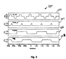
- Figure 3 present simulation results of the CMPFF 200.
- the CMPFF 200 includes a reference voltage generator 202, a reference mirror 203, an input current receiver 204, a current-comparator stage 206, a pulse forming stage (discussed in more detail subsequently) having a pair of inverter amplifiers 210 and 212, pulse formers 214 and 216, a register stage 220 and a static storage cell 222.
- the current-comparator stage 206 compares an input push-pull current I in on a clock (line 240) with a reference current I1 and conditionally amplifies the clock current I in to a full-swing voltage pulse that latches data into the register stage 220, with the data being stored in the static storage cell 222 and output on a line 242.
- the CMPFF 200 is in stark contrast to previous CM logic schemes which utilized large and expensive Rx circuits and buffers to drive storage flip flops.
- the CMPFF 200 By switching on input push-pull currents I in the CMPFF 200 enables use of a relatively simple transmitter Tx circuit (discussed in more detail subsequently) while maintaining a relatively constant bias voltage on interconnects.
- the CMPFF 200 is designed to be sensitive to the unidirectional push current to provide the positive edge trigger needed for operation. This approach lends itself to the use of a complementary current comparator Tx that uses a pull current to produce negative clock edges.
- the reference voltage stage 202 includes a pair of MOS transistors (M1- M2) that creates a first reference current (I ref 1).
- the first reference current (I ref 1) is mirrored by reference mirror 203 M5 to produce a current I1.
- the input current receiver 204 includes a reference voltage generator pair M3-M4 that creates a flip-flop reference current (I ref 2). That flip-flop reference current (I ref 2) is combined with input current I in .
- the resulting current combination is mirrored by M6 of the current-comparator stage 206 to generate a modified current 12.
- the difference between the first reference current I ref 1 and the modified current 12 is applied on line B.
- the reference mirror 203 M5 voltage may use a global reference in place of the reference voltage stage 202. That can increase overall system robustness by reducing transistor mismatches between flip-flops while also saving two transistors per CMPFF 200. Saving those two transistors reduces required static power with a negligible performance penalty.
- the reference mirror 203 M5 voltage would require global distribution and consume metal routing resources. Thus the preferred embodiment is shown in Figure 2 .
- the difference in the mirrored currents I1 and 12 is compared using an inverting amp 210 whose input is at a node B.
- the output of the inverting amp 210 is applies to a CMOS logic level by inverting amp 212.
- inverter pair 214 and 216 generates the required voltage pulse duration using feedback that is applied to M7 of the current-comparator stage 206.
- the feedback applied to M7 quickly pulls node B down. This facilitates generating small voltage pulses having less than 50% duty cycle and results in fewer transistors in the register stage (see below).
- the register stage 220 is similar to a single-phase register as used in J. J. Yuan and C. Svensson, "High-speed CMOS Circuit Technique," Solid-State Circuits, IEEE Journal of, 24(1):62-70 , but requires fewer transistors. It also has a reduced clock load.
- the current-generated voltage pulse (clk_p) triggers storing data in the static storage cell 222.
- the size of M7 of the current-comparator stage 206 is critical to the voltage pulse. Preferably it is a minimum sized NMOS transistor having a unity aspect ratio.
- the width of the generated voltage pulse (clk_p) is also sensitive to the width and amplitude of input current I in .
- the amplitude of I in strongly affects flip flop performance by changing the operating point of M6. This may add extra delays to the generated clk_p.
- the input current should have ⁇ 2.3 uA amplitude and be about 70ps wide.
- Figure 3 illustrates waveforms 300 of the CMPFF 200.
- the input current I in is shown on line 302.
- input current I in involves pulses centered about 0 amperes.
- the resulting clock V clk_p at the output of inverter 216 is shown on line 304.
- Data to be clocked in is shown on line 306.
- the output voltage V Q on line 242 is shown on line 308.
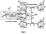
- FIG. 4 illustrates a VLSI device 400 having such transmitter Tx 402. Also shown is a symmetric H-tree network 404 having a balanced set of CMPFFs 200.
- the transmitter Tx 402 receives a traditional voltage CLK from a PLL/clock divider on line 410. The transmitter Tx 402 then supplies a pulsed current to the symmetric H-tree network 404 which has equal impedances in each branch. The symmetric H-tree network 404 distributes current evenly to each CMPFF 200 on each leaf node.
- the transmitter Tx 402 of Figure 4 is similar to previous Tx circuits used in A. Katoch, H. Veendrick, and E, Seevinck, "High speed current-mode signaling circuits for on-chip interconnects," in ISCAS, pages 4138 - 4141, May 2005 and in M. Dave, M. Jain, S. Baghini, and D. Sharma, "A variation tolerant current-mode signaling scheme for on-chip interconnects, IEEE TVLSl, PP(99):1 12, Jan 2012 .
- the transmitter Tx 402 uses a NAND-NOR design.
- the NAND gate 412 uses the CLK signal and a delayed inverted CLK signal, clkb, as inputs to generate a small negative pulse to briefly turn on M1.
- the PMOS transistor briefly sources charge from the supply while the NMOS is off.
- the NOR gate 414 utilizes the negative edge of the CLK and clkb signals to briefly turn on M2.
- the NMOS transistor briefly sinks current while the M1 is off.
- the non-overlapping input signals from the NAND-NOR gates 412, 414 beneficially prevent short circuit current from the transmitter Tx 402.
- the transmitter Tx 402 MI and M2 device sizes are preferably adjusted to supply/sink charge into the symmetric H-tree network 404 CDN.
- the root wires of the symmetric H-tree network 404 carry currents that are distributed to all branches.
- the sizing of the symmetric H-tree network 404 wires is critical for performance and reliability. If the resistance of the wires are too high, the current waveform magnitude and period will be distorted and negatively affect performance of the CMPFF 200.
- the wire width must also consider electromigration effects while carrying the total current to drive all the CMPFF 200 with the required current amplitude and duration.
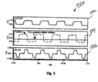
- Figure 5 provides simulated waveforms 500 of the VLSI device 400 that help illustrate how the internal current-to-voltage pulse generation (clk_p) triggers input data capture.
- the CLK input on line 410 is shown on line 502.
- the resulting voltage of the delayed clkb which is applied to NAND-NOR gates 412, 414 is shown on line 504.
- the resulting current clock applied to the CMPFF 200 is shown on line 506.
- the simulation of Figure 5 confirms that a voltage mode input is converted to a constant CDN voltage and a representative push-pull current results at each CMPFF 200. In practice the CMPFFs 200 consumes about 2.9% less silicon area than traditional voltage mode flip flops.
- VLSI device 400 would use 45nm CMOS technology with each CMPFF 200 being compatible with a standard cell library height of 12 horizontal M2 tracks.
- the symmetric H-tree network 404 CDN would span about 1.2mm x 1.2 mm.
- Typical clock frequencies would be between 1.5 and 5 GHz using a 1 V supply and have around 20 ps slew.
Landscapes
- Engineering & Computer Science (AREA)
- Physics & Mathematics (AREA)
- Microelectronics & Electronic Packaging (AREA)
- General Physics & Mathematics (AREA)
- Theoretical Computer Science (AREA)
- Nonlinear Science (AREA)
- General Engineering & Computer Science (AREA)
- Electromagnetism (AREA)
- Radar, Positioning & Navigation (AREA)
- Automation & Control Theory (AREA)
- Manipulation Of Pulses (AREA)
- Logic Circuits (AREA)
- Interface Circuits In Exchanges (AREA)
- Use Of Switch Circuits For Exchanges And Methods Of Control Of Multiplex Exchanges (AREA)
- Analogue/Digital Conversion (AREA)
Claims (11)
- Circuit intégré à très grande échelle (400), comprenant ;un convertisseur d'horloge en mode tension en mode courant (402) recevant une horloge en mode tension (410) et délivrant une horloge en mode courant ;un réseau de distribution d'horloges d'arbre en H (404) ayant au moins une première bascule en mode courant (200) et une seconde bascule en mode courant (200) ; etune interconnexion (A) connectant ladite horloge en mode courant audit réseau de distribution d'horloges d'arbre en H (404) ;dans lequel ledit réseau de distribution d'horloges d'arbre en H (404) distribue symétriquement ladite horloge en mode courant à ladite première bascule en mode courant (200) et à ladite seconde bascule en mode courant (200).
- Circuit intégré à très grande échelle (400) selon la revendication 1, dans lequel ledit convertisseur (402) comporte une porte NON-ET (412) ayant une entrée recevant ladite horloge en mode tension (410), une porte NON-OU (414) ayant une entrée recevant ladite horloge en mode tension (410), et un élément de retard recevant ladite horloge en mode tension (410) et délivrant une horloge en mode tension retardée à ladite porte NON-ET (412) et à ladite porte NON-OU (414).
- Circuit intégré à très grande échelle (400) selon la revendication 2, dans lequel un premier transistor (M1) reçoit la sortie de ladite porte NON-ET (412), ledit premier transistor (M1) étant connecté à (Vdd) et à ladite interconnexion (A).
- Circuit intégré à très grande échelle (400) selon la revendication 3, dans lequel un second transistor (M2) reçoit la sortie de ladite porte NON-OU (414), ledit second transistor (M2) étant connecté à la masse et à ladite interconnexion (A).
- Circuit intégré à très grande échelle (400) selon la revendication 4, dans lequel ladite première bascule en mode courant (200) comporte :un premier miroir de courant (203) pour recevoir une référence de tension et pour produire un premier courant de référence (Iref1) en réponse à ladite référence de tension ;un second miroir de courant pour produire un second courant de référence (Iref2) ;une entrée de courant (Iin) pour modifier ledit second courant de référence (Iref2) ;un comparateur de courant (206) pour produire un courant de différence entre ledit premier courant de référence (Iref1) et ledit second courant de référence modifié (12) ;un amplificateur inverseur (210) pour convertir ledit courant de différence en une tension de niveau logique ;formeur d'impulsions (214, 216) recevant ladite tension de niveau logique et pour appliquer une version retardée audit comparateur de courant (206) pour former ainsi un signal d'horloge ayant une durée d'impulsion ;un étage de registre (220) pour recevoir un signal de données et ledit signal d'horloge ; etune cellule de stockage (222) pour stocker des données lorsque ledit signal d'horloge se produit.
- Circuit intégré à très grande échelle (400) selon la revendication 5, dans lequel ladite référence de tension est produite par une référence de courant.
- Circuit intégré à très grande échelle (400) selon la revendication 5, dans lequel ladite référence de tension est appliquée de manière externe.
- Circuit intégré à très grande échelle (400) selon la revendication 5, dans lequel ledit premier miroir de courant (203) est fabriqué à l'aide de la technologie CMOS.
- Circuit intégré à très grande échelle (400) selon la revendication 5, dans lequel ladite technologie CMOS est une technologie CMOS de 45 mm.
- Circuit intégré à très grande échelle (400) selon la revendication 5, dans lequel ladite première bascule en mode courant (200) fait partie d'un réseau de distribution d'horloges à arbre en H (404).
- Circuit intégré à très grande échelle (400) selon la revendication 10, dans lequel ladite première bascule en mode courant (200) fait partie d'un réseau de distribution d'horloges à arbre en H équilibré (404).
Applications Claiming Priority (2)
| Application Number | Priority Date | Filing Date | Title |
|---|---|---|---|
| US201461933204P | 2014-01-29 | 2014-01-29 | |
| PCT/US2015/013572 WO2015116843A2 (fr) | 2014-01-29 | 2015-01-29 | Distribution d'horloge en mode courant |
Publications (3)
| Publication Number | Publication Date |
|---|---|
| EP3100361A2 EP3100361A2 (fr) | 2016-12-07 |
| EP3100361A4 EP3100361A4 (fr) | 2017-11-29 |
| EP3100361B1 true EP3100361B1 (fr) | 2022-03-09 |
Family
ID=53757915
Family Applications (1)
| Application Number | Title | Priority Date | Filing Date |
|---|---|---|---|
| EP15743426.7A Active EP3100361B1 (fr) | 2014-01-29 | 2015-01-29 | Distribution d'horloge en mode courant |
Country Status (5)
| Country | Link |
|---|---|
| US (2) | US9787293B2 (fr) |
| EP (1) | EP3100361B1 (fr) |
| CN (1) | CN106134084B (fr) |
| CA (1) | CA2939453A1 (fr) |
| WO (1) | WO2015116843A2 (fr) |
Families Citing this family (3)
| Publication number | Priority date | Publication date | Assignee | Title |
|---|---|---|---|---|
| WO2015116843A2 (fr) * | 2014-01-29 | 2015-08-06 | Matthew Guthaus | Distribution d'horloge en mode courant |
| US10712769B2 (en) | 2017-08-16 | 2020-07-14 | Oracle International Corporation | Method and apparatus for clock signal distribution |
| US10691162B2 (en) * | 2018-06-15 | 2020-06-23 | The Regents Of The University Of California | System and method for a hybrid current-mode and voltage-mode integrated circuit |
Family Cites Families (19)
| Publication number | Priority date | Publication date | Assignee | Title |
|---|---|---|---|---|
| US4719375A (en) * | 1986-05-09 | 1988-01-12 | The United States Of America As Represented By The United States Department Of Energy | High resolution digital delay timer |
| US5109168A (en) * | 1991-02-27 | 1992-04-28 | Sun Microsystems, Inc. | Method and apparatus for the design and optimization of a balanced tree for clock distribution in computer integrated circuits |
| US5557224A (en) * | 1994-04-15 | 1996-09-17 | International Business Machines Corporation | Apparatus and method for generating a phase-controlled clock signal |
| US5889431A (en) * | 1997-06-26 | 1999-03-30 | The Aerospace Corporation | Current mode transistor circuit method |
| US6897699B1 (en) * | 2002-07-19 | 2005-05-24 | Rambus Inc. | Clock distribution network with process, supply-voltage, and temperature compensation |
| US6768655B1 (en) * | 2003-02-03 | 2004-07-27 | System General Corp. | Discontinuous mode PFC controller having a power saving modulator and operation method thereof |
| US7187222B2 (en) * | 2004-12-17 | 2007-03-06 | Seiko Epson Corporation | CMOS master/slave flip-flop with integrated multiplexor |
| DE102005043376B4 (de) * | 2005-09-12 | 2013-08-01 | Austriamicrosystems Ag | Oszillatoranordnung und Verfahren zum Erzeugen eines periodischen Signals |
| TWI365282B (en) * | 2008-01-22 | 2012-06-01 | Feature Integration Technology Inc | Current control apparatus applied to transistor |
| JP5195182B2 (ja) * | 2008-09-04 | 2013-05-08 | 株式会社リコー | 電流モード制御型スイッチングレギュレータ |
| US7839161B2 (en) | 2009-01-22 | 2010-11-23 | Broadcom Corporation | Low-jitter high-frequency clock channel |
| US9152161B2 (en) * | 2011-12-20 | 2015-10-06 | Maxim Integrated Products, Inc. | Maintain power signature (MPS) powered device (PD) |
| TWI449342B (zh) * | 2012-01-20 | 2014-08-11 | Silicon Motion Inc | 串化器及資料串化方法 |
| US8836394B2 (en) * | 2012-03-26 | 2014-09-16 | Rambus Inc. | Method and apparatus for source-synchronous signaling |
| US8629715B1 (en) | 2012-08-28 | 2014-01-14 | Cambridge Silicon Radio Limited | Clock distribution scheme |
| KR101965632B1 (ko) * | 2012-09-07 | 2019-04-05 | 삼성전자 주식회사 | 아날로그-디지털 변환 회로, 이를 포함하는 이미지 센서, 및 그 동작 방법 |
| WO2015116843A2 (fr) * | 2014-01-29 | 2015-08-06 | Matthew Guthaus | Distribution d'horloge en mode courant |
| JP5909294B1 (ja) * | 2015-03-11 | 2016-04-26 | 力晶科技股▲ふん▼有限公司 | 不揮発性記憶装置のための書き込み回路及び方法、並びに不揮発性記憶装置 |
| US9484893B1 (en) * | 2015-04-20 | 2016-11-01 | Telefonaktiebolaget Lm Ericsson (Publ) | Clock generation circuit with fast-startup standby mode |
-
2015
- 2015-01-29 WO PCT/US2015/013572 patent/WO2015116843A2/fr not_active Ceased
- 2015-01-29 EP EP15743426.7A patent/EP3100361B1/fr active Active
- 2015-01-29 CA CA2939453A patent/CA2939453A1/fr not_active Abandoned
- 2015-01-29 US US15/115,382 patent/US9787293B2/en active Active
- 2015-01-29 CN CN201580011228.3A patent/CN106134084B/zh not_active Expired - Fee Related
-
2017
- 2017-09-11 US US15/701,133 patent/US10097168B2/en active Active
Also Published As
| Publication number | Publication date |
|---|---|
| CA2939453A1 (fr) | 2015-08-06 |
| US20180076799A1 (en) | 2018-03-15 |
| US10097168B2 (en) | 2018-10-09 |
| CN106134084A (zh) | 2016-11-16 |
| WO2015116843A2 (fr) | 2015-08-06 |
| EP3100361A4 (fr) | 2017-11-29 |
| US9787293B2 (en) | 2017-10-10 |
| US20170012614A1 (en) | 2017-01-12 |
| CN106134084B (zh) | 2019-11-29 |
| WO2015116843A3 (fr) | 2015-11-12 |
| EP3100361A2 (fr) | 2016-12-07 |
Similar Documents
| Publication | Publication Date | Title |
|---|---|---|
| US10840920B2 (en) | Method and apparatus for source-synchronous signaling | |
| TWI514767B (zh) | 用於差動發信的資料驅動充電泵傳送器 | |
| TWI516031B (zh) | 接地參考單端發信 | |
| US8415980B2 (en) | Serializing transmitter | |
| Islam et al. | Low-power clock distribution using a current-pulsed clocked flip-flop | |
| US10097168B2 (en) | Current-mode clock distribution | |
| CN104617922B (zh) | 高速低功耗多阈值异步置位复位d型触发器 | |
| Wei et al. | A 10-Gb/s/ch, 0.6-pj/bit/mm power scalable rapid-on/off transceiver for on-chip energy proportional interconnects | |
| CN104617923B (zh) | 高速低功耗多阈值d型触发器 | |
| Islam et al. | Differential current-mode clock distribution | |
| Dazzi et al. | Sub-mW multi-Gbps chip-to-chip communication Links for Ultra-Low Power IoT end-nodes | |
| Seo et al. | A 20-Gb/s/Pin Compact Single-Ended DCC-Less DECS Transceiver With CDR-Less RX Front-End for On-Chip Links | |
| Jaiswal et al. | Low-power high-speed on-chip asynchronous wave-pipelined CML SerDes | |
| Hien et al. | Design of a wave-pipelined serializer-deserializer with an asynchronous protocol for high speed interfaces | |
| Dave et al. | Energy efficient current-mode signaling scheme | |
| CN104639116B (zh) | 高速低功耗多阈值同步置位复位d型触发器 | |
| US20100040122A1 (en) | Simultaneous bi-directional data transfer | |
| Nieminen et al. | A 5.8-Gbps low-noise scalable low-voltage signaling serial link transmitter for MIPI M-PHY in 40-nm CMOS | |
| Anita et al. | Review of clock distribution networks | |
| Ho et al. | Low delay-variation sub-/near-threshold asynchronous-to-synchronous interface controller for GALS Network-on-Chips | |
| Song et al. | Low-Power 10-Gb/s Transmitter for High-Speed Graphic DRAMs Using 0.18-$\mu\hbox {m} $ CMOS Technology | |
| Duraivel et al. | Proficient technique for high performance very large-scale integration system to amend clock gated dual edge triggered sense amplifier flip-flop with less dissipation of power leakage | |
| Prabakaran et al. | A low power and high performance on-chip interconnect using current mode signalling scheme | |
| Hwang et al. | An add-on type real-time jitter tolerance enhancer for digital communication receivers | |
| Rajesh et al. | Design of voltage scaled level converters in low power clock distribution networks |
Legal Events
| Date | Code | Title | Description |
|---|---|---|---|
| PUAI | Public reference made under article 153(3) epc to a published international application that has entered the european phase |
Free format text: ORIGINAL CODE: 0009012 |
|
| STAA | Information on the status of an ep patent application or granted ep patent |
Free format text: STATUS: REQUEST FOR EXAMINATION WAS MADE |
|
| 17P | Request for examination filed |
Effective date: 20160818 |
|
| AK | Designated contracting states |
Kind code of ref document: A2 Designated state(s): AL AT BE BG CH CY CZ DE DK EE ES FI FR GB GR HR HU IE IS IT LI LT LU LV MC MK MT NL NO PL PT RO RS SE SI SK SM TR |
|
| AX | Request for extension of the european patent |
Extension state: BA ME |
|
| DAX | Request for extension of the european patent (deleted) | ||
| A4 | Supplementary search report drawn up and despatched |
Effective date: 20171027 |
|
| RIC1 | Information provided on ipc code assigned before grant |
Ipc: H03M 9/00 20060101AFI20171023BHEP Ipc: G06F 1/10 20060101ALI20171023BHEP |
|
| STAA | Information on the status of an ep patent application or granted ep patent |
Free format text: STATUS: EXAMINATION IS IN PROGRESS |
|
| 17Q | First examination report despatched |
Effective date: 20200218 |
|
| GRAP | Despatch of communication of intention to grant a patent |
Free format text: ORIGINAL CODE: EPIDOSNIGR1 |
|
| STAA | Information on the status of an ep patent application or granted ep patent |
Free format text: STATUS: GRANT OF PATENT IS INTENDED |
|
| INTG | Intention to grant announced |
Effective date: 20211202 |
|
| GRAS | Grant fee paid |
Free format text: ORIGINAL CODE: EPIDOSNIGR3 |
|
| GRAA | (expected) grant |
Free format text: ORIGINAL CODE: 0009210 |
|
| STAA | Information on the status of an ep patent application or granted ep patent |
Free format text: STATUS: THE PATENT HAS BEEN GRANTED |
|
| AK | Designated contracting states |
Kind code of ref document: B1 Designated state(s): AL AT BE BG CH CY CZ DE DK EE ES FI FR GB GR HR HU IE IS IT LI LT LU LV MC MK MT NL NO PL PT RO RS SE SI SK SM TR |
|
| REG | Reference to a national code |
Ref country code: GB Ref legal event code: FG4D |
|
| REG | Reference to a national code |
Ref country code: CH Ref legal event code: EP Ref country code: AT Ref legal event code: REF Ref document number: 1474983 Country of ref document: AT Kind code of ref document: T Effective date: 20220315 |
|
| REG | Reference to a national code |
Ref country code: IE Ref legal event code: FG4D |
|
| REG | Reference to a national code |
Ref country code: DE Ref legal event code: R096 Ref document number: 602015077404 Country of ref document: DE |
|
| REG | Reference to a national code |
Ref country code: LT Ref legal event code: MG9D |
|
| REG | Reference to a national code |
Ref country code: NL Ref legal event code: MP Effective date: 20220309 |
|
| PG25 | Lapsed in a contracting state [announced via postgrant information from national office to epo] |
Ref country code: SE Free format text: LAPSE BECAUSE OF FAILURE TO SUBMIT A TRANSLATION OF THE DESCRIPTION OR TO PAY THE FEE WITHIN THE PRESCRIBED TIME-LIMIT Effective date: 20220309 Ref country code: RS Free format text: LAPSE BECAUSE OF FAILURE TO SUBMIT A TRANSLATION OF THE DESCRIPTION OR TO PAY THE FEE WITHIN THE PRESCRIBED TIME-LIMIT Effective date: 20220309 Ref country code: NO Free format text: LAPSE BECAUSE OF FAILURE TO SUBMIT A TRANSLATION OF THE DESCRIPTION OR TO PAY THE FEE WITHIN THE PRESCRIBED TIME-LIMIT Effective date: 20220609 Ref country code: LT Free format text: LAPSE BECAUSE OF FAILURE TO SUBMIT A TRANSLATION OF THE DESCRIPTION OR TO PAY THE FEE WITHIN THE PRESCRIBED TIME-LIMIT Effective date: 20220309 Ref country code: HR Free format text: LAPSE BECAUSE OF FAILURE TO SUBMIT A TRANSLATION OF THE DESCRIPTION OR TO PAY THE FEE WITHIN THE PRESCRIBED TIME-LIMIT Effective date: 20220309 Ref country code: BG Free format text: LAPSE BECAUSE OF FAILURE TO SUBMIT A TRANSLATION OF THE DESCRIPTION OR TO PAY THE FEE WITHIN THE PRESCRIBED TIME-LIMIT Effective date: 20220609 |
|
| REG | Reference to a national code |
Ref country code: AT Ref legal event code: MK05 Ref document number: 1474983 Country of ref document: AT Kind code of ref document: T Effective date: 20220309 |
|
| PG25 | Lapsed in a contracting state [announced via postgrant information from national office to epo] |
Ref country code: LV Free format text: LAPSE BECAUSE OF FAILURE TO SUBMIT A TRANSLATION OF THE DESCRIPTION OR TO PAY THE FEE WITHIN THE PRESCRIBED TIME-LIMIT Effective date: 20220309 Ref country code: GR Free format text: LAPSE BECAUSE OF FAILURE TO SUBMIT A TRANSLATION OF THE DESCRIPTION OR TO PAY THE FEE WITHIN THE PRESCRIBED TIME-LIMIT Effective date: 20220610 Ref country code: FI Free format text: LAPSE BECAUSE OF FAILURE TO SUBMIT A TRANSLATION OF THE DESCRIPTION OR TO PAY THE FEE WITHIN THE PRESCRIBED TIME-LIMIT Effective date: 20220309 |
|
| PG25 | Lapsed in a contracting state [announced via postgrant information from national office to epo] |
Ref country code: NL Free format text: LAPSE BECAUSE OF FAILURE TO SUBMIT A TRANSLATION OF THE DESCRIPTION OR TO PAY THE FEE WITHIN THE PRESCRIBED TIME-LIMIT Effective date: 20220309 |
|
| PG25 | Lapsed in a contracting state [announced via postgrant information from national office to epo] |
Ref country code: SM Free format text: LAPSE BECAUSE OF FAILURE TO SUBMIT A TRANSLATION OF THE DESCRIPTION OR TO PAY THE FEE WITHIN THE PRESCRIBED TIME-LIMIT Effective date: 20220309 Ref country code: SK Free format text: LAPSE BECAUSE OF FAILURE TO SUBMIT A TRANSLATION OF THE DESCRIPTION OR TO PAY THE FEE WITHIN THE PRESCRIBED TIME-LIMIT Effective date: 20220309 Ref country code: RO Free format text: LAPSE BECAUSE OF FAILURE TO SUBMIT A TRANSLATION OF THE DESCRIPTION OR TO PAY THE FEE WITHIN THE PRESCRIBED TIME-LIMIT Effective date: 20220309 Ref country code: PT Free format text: LAPSE BECAUSE OF FAILURE TO SUBMIT A TRANSLATION OF THE DESCRIPTION OR TO PAY THE FEE WITHIN THE PRESCRIBED TIME-LIMIT Effective date: 20220711 Ref country code: ES Free format text: LAPSE BECAUSE OF FAILURE TO SUBMIT A TRANSLATION OF THE DESCRIPTION OR TO PAY THE FEE WITHIN THE PRESCRIBED TIME-LIMIT Effective date: 20220309 Ref country code: EE Free format text: LAPSE BECAUSE OF FAILURE TO SUBMIT A TRANSLATION OF THE DESCRIPTION OR TO PAY THE FEE WITHIN THE PRESCRIBED TIME-LIMIT Effective date: 20220309 Ref country code: CZ Free format text: LAPSE BECAUSE OF FAILURE TO SUBMIT A TRANSLATION OF THE DESCRIPTION OR TO PAY THE FEE WITHIN THE PRESCRIBED TIME-LIMIT Effective date: 20220309 Ref country code: AT Free format text: LAPSE BECAUSE OF FAILURE TO SUBMIT A TRANSLATION OF THE DESCRIPTION OR TO PAY THE FEE WITHIN THE PRESCRIBED TIME-LIMIT Effective date: 20220309 |
|
| PG25 | Lapsed in a contracting state [announced via postgrant information from national office to epo] |
Ref country code: PL Free format text: LAPSE BECAUSE OF FAILURE TO SUBMIT A TRANSLATION OF THE DESCRIPTION OR TO PAY THE FEE WITHIN THE PRESCRIBED TIME-LIMIT Effective date: 20220309 Ref country code: IS Free format text: LAPSE BECAUSE OF FAILURE TO SUBMIT A TRANSLATION OF THE DESCRIPTION OR TO PAY THE FEE WITHIN THE PRESCRIBED TIME-LIMIT Effective date: 20220709 Ref country code: AL Free format text: LAPSE BECAUSE OF FAILURE TO SUBMIT A TRANSLATION OF THE DESCRIPTION OR TO PAY THE FEE WITHIN THE PRESCRIBED TIME-LIMIT Effective date: 20220309 |
|
| REG | Reference to a national code |
Ref country code: DE Ref legal event code: R097 Ref document number: 602015077404 Country of ref document: DE |
|
| PLBE | No opposition filed within time limit |
Free format text: ORIGINAL CODE: 0009261 |
|
| STAA | Information on the status of an ep patent application or granted ep patent |
Free format text: STATUS: NO OPPOSITION FILED WITHIN TIME LIMIT |
|
| PG25 | Lapsed in a contracting state [announced via postgrant information from national office to epo] |
Ref country code: DK Free format text: LAPSE BECAUSE OF FAILURE TO SUBMIT A TRANSLATION OF THE DESCRIPTION OR TO PAY THE FEE WITHIN THE PRESCRIBED TIME-LIMIT Effective date: 20220309 |
|
| 26N | No opposition filed |
Effective date: 20221212 |
|
| PG25 | Lapsed in a contracting state [announced via postgrant information from national office to epo] |
Ref country code: SI Free format text: LAPSE BECAUSE OF FAILURE TO SUBMIT A TRANSLATION OF THE DESCRIPTION OR TO PAY THE FEE WITHIN THE PRESCRIBED TIME-LIMIT Effective date: 20220309 |
|
| P01 | Opt-out of the competence of the unified patent court (upc) registered |
Effective date: 20230530 |
|
| PG25 | Lapsed in a contracting state [announced via postgrant information from national office to epo] |
Ref country code: IT Free format text: LAPSE BECAUSE OF FAILURE TO SUBMIT A TRANSLATION OF THE DESCRIPTION OR TO PAY THE FEE WITHIN THE PRESCRIBED TIME-LIMIT Effective date: 20220309 |
|
| REG | Reference to a national code |
Ref country code: CH Ref legal event code: PL |
|
| PG25 | Lapsed in a contracting state [announced via postgrant information from national office to epo] |
Ref country code: LU Free format text: LAPSE BECAUSE OF NON-PAYMENT OF DUE FEES Effective date: 20230129 |
|
| REG | Reference to a national code |
Ref country code: BE Ref legal event code: MM Effective date: 20230131 |
|
| PG25 | Lapsed in a contracting state [announced via postgrant information from national office to epo] |
Ref country code: CH Free format text: LAPSE BECAUSE OF NON-PAYMENT OF DUE FEES Effective date: 20230131 Ref country code: LI Free format text: LAPSE BECAUSE OF NON-PAYMENT OF DUE FEES Effective date: 20230131 |
|
| PG25 | Lapsed in a contracting state [announced via postgrant information from national office to epo] |
Ref country code: BE Free format text: LAPSE BECAUSE OF NON-PAYMENT OF DUE FEES Effective date: 20230131 |
|
| PG25 | Lapsed in a contracting state [announced via postgrant information from national office to epo] |
Ref country code: IE Free format text: LAPSE BECAUSE OF NON-PAYMENT OF DUE FEES Effective date: 20230129 |
|
| PGFP | Annual fee paid to national office [announced via postgrant information from national office to epo] |
Ref country code: DE Payment date: 20240129 Year of fee payment: 10 Ref country code: GB Payment date: 20240129 Year of fee payment: 10 |
|
| PGFP | Annual fee paid to national office [announced via postgrant information from national office to epo] |
Ref country code: FR Payment date: 20240125 Year of fee payment: 10 |
|
| PG25 | Lapsed in a contracting state [announced via postgrant information from national office to epo] |
Ref country code: MC Free format text: LAPSE BECAUSE OF FAILURE TO SUBMIT A TRANSLATION OF THE DESCRIPTION OR TO PAY THE FEE WITHIN THE PRESCRIBED TIME-LIMIT Effective date: 20220309 |
|
| PG25 | Lapsed in a contracting state [announced via postgrant information from national office to epo] |
Ref country code: MC Free format text: LAPSE BECAUSE OF FAILURE TO SUBMIT A TRANSLATION OF THE DESCRIPTION OR TO PAY THE FEE WITHIN THE PRESCRIBED TIME-LIMIT Effective date: 20220309 |
|
| PG25 | Lapsed in a contracting state [announced via postgrant information from national office to epo] |
Ref country code: CY Free format text: LAPSE BECAUSE OF FAILURE TO SUBMIT A TRANSLATION OF THE DESCRIPTION OR TO PAY THE FEE WITHIN THE PRESCRIBED TIME-LIMIT; INVALID AB INITIO Effective date: 20150129 |
|
| REG | Reference to a national code |
Ref country code: DE Ref legal event code: R119 Ref document number: 602015077404 Country of ref document: DE |
|
| PG25 | Lapsed in a contracting state [announced via postgrant information from national office to epo] |
Ref country code: HU Free format text: LAPSE BECAUSE OF FAILURE TO SUBMIT A TRANSLATION OF THE DESCRIPTION OR TO PAY THE FEE WITHIN THE PRESCRIBED TIME-LIMIT; INVALID AB INITIO Effective date: 20150129 |
|
| GBPC | Gb: european patent ceased through non-payment of renewal fee |
Effective date: 20250129 |
|
| PG25 | Lapsed in a contracting state [announced via postgrant information from national office to epo] |
Ref country code: DE Free format text: LAPSE BECAUSE OF NON-PAYMENT OF DUE FEES Effective date: 20250801 |
|
| PG25 | Lapsed in a contracting state [announced via postgrant information from national office to epo] |
Ref country code: GB Free format text: LAPSE BECAUSE OF NON-PAYMENT OF DUE FEES Effective date: 20250129 |
|
| PG25 | Lapsed in a contracting state [announced via postgrant information from national office to epo] |
Ref country code: FR Free format text: LAPSE BECAUSE OF NON-PAYMENT OF DUE FEES Effective date: 20250131 |
|
| PG25 | Lapsed in a contracting state [announced via postgrant information from national office to epo] |
Ref country code: TR Free format text: LAPSE BECAUSE OF FAILURE TO SUBMIT A TRANSLATION OF THE DESCRIPTION OR TO PAY THE FEE WITHIN THE PRESCRIBED TIME-LIMIT Effective date: 20220309 |