EP3101681B1 - Pièce à usiner formant plaquette, matériau adhésif provisoire pour usinage de plaquette, et procédé de fabrication de plaquette mince - Google Patents
Pièce à usiner formant plaquette, matériau adhésif provisoire pour usinage de plaquette, et procédé de fabrication de plaquette mince Download PDFInfo
- Publication number
- EP3101681B1 EP3101681B1 EP15743005.9A EP15743005A EP3101681B1 EP 3101681 B1 EP3101681 B1 EP 3101681B1 EP 15743005 A EP15743005 A EP 15743005A EP 3101681 B1 EP3101681 B1 EP 3101681B1
- Authority
- EP
- European Patent Office
- Prior art keywords
- wafer
- polymer layer
- layer
- temporary adhesive
- siloxane
- Prior art date
- Legal status (The legal status is an assumption and is not a legal conclusion. Google has not performed a legal analysis and makes no representation as to the accuracy of the status listed.)
- Active
Links
- IOYLGBVUYSKPGB-XRVBUDJMSA-N C/C=[Cl]\C=C/C(OC[C@H]1OC1)=C Chemical compound C/C=[Cl]\C=C/C(OC[C@H]1OC1)=C IOYLGBVUYSKPGB-XRVBUDJMSA-N 0.000 description 1
Images

Classifications
-
- C—CHEMISTRY; METALLURGY
- C09—DYES; PAINTS; POLISHES; NATURAL RESINS; ADHESIVES; COMPOSITIONS NOT OTHERWISE PROVIDED FOR; APPLICATIONS OF MATERIALS NOT OTHERWISE PROVIDED FOR
- C09J—ADHESIVES; NON-MECHANICAL ASPECTS OF ADHESIVE PROCESSES IN GENERAL; ADHESIVE PROCESSES NOT PROVIDED FOR ELSEWHERE; USE OF MATERIALS AS ADHESIVES
- C09J183/00—Adhesives based on macromolecular compounds obtained by reactions forming in the main chain of the macromolecule a linkage containing silicon, with or without sulfur, nitrogen, oxygen, or carbon only; Adhesives based on derivatives of such polymers
- C09J183/04—Polysiloxanes
-
- C—CHEMISTRY; METALLURGY
- C09—DYES; PAINTS; POLISHES; NATURAL RESINS; ADHESIVES; COMPOSITIONS NOT OTHERWISE PROVIDED FOR; APPLICATIONS OF MATERIALS NOT OTHERWISE PROVIDED FOR
- C09J—ADHESIVES; NON-MECHANICAL ASPECTS OF ADHESIVE PROCESSES IN GENERAL; ADHESIVE PROCESSES NOT PROVIDED FOR ELSEWHERE; USE OF MATERIALS AS ADHESIVES
- C09J7/00—Adhesives in the form of films or foils
- C09J7/40—Adhesives in the form of films or foils characterised by release liners
-
- B—PERFORMING OPERATIONS; TRANSPORTING
- B32—LAYERED PRODUCTS
- B32B—LAYERED PRODUCTS, i.e. PRODUCTS BUILT-UP OF STRATA OF FLAT OR NON-FLAT, e.g. CELLULAR OR HONEYCOMB, FORM
- B32B27/00—Layered products comprising a layer of synthetic resin
- B32B27/28—Layered products comprising a layer of synthetic resin comprising synthetic resins not wholly covered by any one of the sub-groups B32B27/30 - B32B27/42
- B32B27/283—Layered products comprising a layer of synthetic resin comprising synthetic resins not wholly covered by any one of the sub-groups B32B27/30 - B32B27/42 comprising polysiloxanes
-
- C—CHEMISTRY; METALLURGY
- C08—ORGANIC MACROMOLECULAR COMPOUNDS; THEIR PREPARATION OR CHEMICAL WORKING-UP; COMPOSITIONS BASED THEREON
- C08L—COMPOSITIONS OF MACROMOLECULAR COMPOUNDS
- C08L83/00—Compositions of macromolecular compounds obtained by reactions forming in the main chain of the macromolecule a linkage containing silicon with or without sulfur, nitrogen, oxygen or carbon only; Compositions of derivatives of such polymers
- C08L83/04—Polysiloxanes
-
- C—CHEMISTRY; METALLURGY
- C09—DYES; PAINTS; POLISHES; NATURAL RESINS; ADHESIVES; COMPOSITIONS NOT OTHERWISE PROVIDED FOR; APPLICATIONS OF MATERIALS NOT OTHERWISE PROVIDED FOR
- C09J—ADHESIVES; NON-MECHANICAL ASPECTS OF ADHESIVE PROCESSES IN GENERAL; ADHESIVE PROCESSES NOT PROVIDED FOR ELSEWHERE; USE OF MATERIALS AS ADHESIVES
- C09J183/00—Adhesives based on macromolecular compounds obtained by reactions forming in the main chain of the macromolecule a linkage containing silicon, with or without sulfur, nitrogen, oxygen, or carbon only; Adhesives based on derivatives of such polymers
- C09J183/10—Block or graft copolymers containing polysiloxane sequences
-
- C—CHEMISTRY; METALLURGY
- C09—DYES; PAINTS; POLISHES; NATURAL RESINS; ADHESIVES; COMPOSITIONS NOT OTHERWISE PROVIDED FOR; APPLICATIONS OF MATERIALS NOT OTHERWISE PROVIDED FOR
- C09J—ADHESIVES; NON-MECHANICAL ASPECTS OF ADHESIVE PROCESSES IN GENERAL; ADHESIVE PROCESSES NOT PROVIDED FOR ELSEWHERE; USE OF MATERIALS AS ADHESIVES
- C09J183/00—Adhesives based on macromolecular compounds obtained by reactions forming in the main chain of the macromolecule a linkage containing silicon, with or without sulfur, nitrogen, oxygen, or carbon only; Adhesives based on derivatives of such polymers
- C09J183/14—Adhesives based on macromolecular compounds obtained by reactions forming in the main chain of the macromolecule a linkage containing silicon, with or without sulfur, nitrogen, oxygen, or carbon only; Adhesives based on derivatives of such polymers in which at least two but not all the silicon atoms are connected by linkages other than oxygen atoms
-
- H—ELECTRICITY
- H10—SEMICONDUCTOR DEVICES; ELECTRIC SOLID-STATE DEVICES NOT OTHERWISE PROVIDED FOR
- H10P—GENERIC PROCESSES OR APPARATUS FOR THE MANUFACTURE OR TREATMENT OF DEVICES COVERED BY CLASS H10
- H10P14/00—Formation of materials, e.g. in the shape of layers or pillars
- H10P14/60—Formation of materials, e.g. in the shape of layers or pillars of insulating materials
- H10P14/63—Formation of materials, e.g. in the shape of layers or pillars of insulating materials characterised by the formation processes
- H10P14/6302—Non-deposition formation processes
- H10P14/6322—Formation by thermal treatments
-
- H—ELECTRICITY
- H10—SEMICONDUCTOR DEVICES; ELECTRIC SOLID-STATE DEVICES NOT OTHERWISE PROVIDED FOR
- H10P—GENERIC PROCESSES OR APPARATUS FOR THE MANUFACTURE OR TREATMENT OF DEVICES COVERED BY CLASS H10
- H10P52/00—Grinding, lapping or polishing of wafers, substrates or parts of devices
-
- H—ELECTRICITY
- H10—SEMICONDUCTOR DEVICES; ELECTRIC SOLID-STATE DEVICES NOT OTHERWISE PROVIDED FOR
- H10P—GENERIC PROCESSES OR APPARATUS FOR THE MANUFACTURE OR TREATMENT OF DEVICES COVERED BY CLASS H10
- H10P72/00—Handling or holding of wafers, substrates or devices during manufacture or treatment thereof
- H10P72/70—Handling or holding of wafers, substrates or devices during manufacture or treatment thereof for supporting or gripping
- H10P72/74—Handling or holding of wafers, substrates or devices during manufacture or treatment thereof for supporting or gripping using temporarily an auxiliary support
-
- H—ELECTRICITY
- H10—SEMICONDUCTOR DEVICES; ELECTRIC SOLID-STATE DEVICES NOT OTHERWISE PROVIDED FOR
- H10P—GENERIC PROCESSES OR APPARATUS FOR THE MANUFACTURE OR TREATMENT OF DEVICES COVERED BY CLASS H10
- H10P72/00—Handling or holding of wafers, substrates or devices during manufacture or treatment thereof
- H10P72/70—Handling or holding of wafers, substrates or devices during manufacture or treatment thereof for supporting or gripping
- H10P72/74—Handling or holding of wafers, substrates or devices during manufacture or treatment thereof for supporting or gripping using temporarily an auxiliary support
- H10P72/7448—Handling or holding of wafers, substrates or devices during manufacture or treatment thereof for supporting or gripping using temporarily an auxiliary support the bond interface between the auxiliary support and the wafer comprising two or more, e.g. multilayer adhesive or adhesive and release layer
-
- H—ELECTRICITY
- H10—SEMICONDUCTOR DEVICES; ELECTRIC SOLID-STATE DEVICES NOT OTHERWISE PROVIDED FOR
- H10P—GENERIC PROCESSES OR APPARATUS FOR THE MANUFACTURE OR TREATMENT OF DEVICES COVERED BY CLASS H10
- H10P72/00—Handling or holding of wafers, substrates or devices during manufacture or treatment thereof
- H10P72/70—Handling or holding of wafers, substrates or devices during manufacture or treatment thereof for supporting or gripping
- H10P72/74—Handling or holding of wafers, substrates or devices during manufacture or treatment thereof for supporting or gripping using temporarily an auxiliary support
- H10P72/7448—Handling or holding of wafers, substrates or devices during manufacture or treatment thereof for supporting or gripping using temporarily an auxiliary support the bond interface between the auxiliary support and the wafer comprising two or more, e.g. multilayer adhesive or adhesive and release layer
- H10P72/745—Handling or holding of wafers, substrates or devices during manufacture or treatment thereof for supporting or gripping using temporarily an auxiliary support the bond interface between the auxiliary support and the wafer comprising two or more, e.g. multilayer adhesive or adhesive and release layer the bond interface between the auxiliary support and the wafer comprises three or more layers
-
- C—CHEMISTRY; METALLURGY
- C08—ORGANIC MACROMOLECULAR COMPOUNDS; THEIR PREPARATION OR CHEMICAL WORKING-UP; COMPOSITIONS BASED THEREON
- C08G—MACROMOLECULAR COMPOUNDS OBTAINED OTHERWISE THAN BY REACTIONS ONLY INVOLVING UNSATURATED CARBON-TO-CARBON BONDS
- C08G77/00—Macromolecular compounds obtained by reactions forming a linkage containing silicon with or without sulfur, nitrogen, oxygen or carbon in the main chain of the macromolecule
- C08G77/04—Polysiloxanes
-
- C—CHEMISTRY; METALLURGY
- C08—ORGANIC MACROMOLECULAR COMPOUNDS; THEIR PREPARATION OR CHEMICAL WORKING-UP; COMPOSITIONS BASED THEREON
- C08G—MACROMOLECULAR COMPOUNDS OBTAINED OTHERWISE THAN BY REACTIONS ONLY INVOLVING UNSATURATED CARBON-TO-CARBON BONDS
- C08G77/00—Macromolecular compounds obtained by reactions forming a linkage containing silicon with or without sulfur, nitrogen, oxygen or carbon in the main chain of the macromolecule
- C08G77/04—Polysiloxanes
- C08G77/12—Polysiloxanes containing silicon bound to hydrogen
-
- C—CHEMISTRY; METALLURGY
- C08—ORGANIC MACROMOLECULAR COMPOUNDS; THEIR PREPARATION OR CHEMICAL WORKING-UP; COMPOSITIONS BASED THEREON
- C08G—MACROMOLECULAR COMPOUNDS OBTAINED OTHERWISE THAN BY REACTIONS ONLY INVOLVING UNSATURATED CARBON-TO-CARBON BONDS
- C08G77/00—Macromolecular compounds obtained by reactions forming a linkage containing silicon with or without sulfur, nitrogen, oxygen or carbon in the main chain of the macromolecule
- C08G77/48—Macromolecular compounds obtained by reactions forming a linkage containing silicon with or without sulfur, nitrogen, oxygen or carbon in the main chain of the macromolecule in which at least two but not all the silicon atoms are connected by linkages other than oxygen atoms
- C08G77/50—Macromolecular compounds obtained by reactions forming a linkage containing silicon with or without sulfur, nitrogen, oxygen or carbon in the main chain of the macromolecule in which at least two but not all the silicon atoms are connected by linkages other than oxygen atoms by carbon linkages
-
- C—CHEMISTRY; METALLURGY
- C09—DYES; PAINTS; POLISHES; NATURAL RESINS; ADHESIVES; COMPOSITIONS NOT OTHERWISE PROVIDED FOR; APPLICATIONS OF MATERIALS NOT OTHERWISE PROVIDED FOR
- C09J—ADHESIVES; NON-MECHANICAL ASPECTS OF ADHESIVE PROCESSES IN GENERAL; ADHESIVE PROCESSES NOT PROVIDED FOR ELSEWHERE; USE OF MATERIALS AS ADHESIVES
- C09J2203/00—Applications of adhesives in processes or use of adhesives in the form of films or foils
- C09J2203/326—Applications of adhesives in processes or use of adhesives in the form of films or foils for bonding electronic components such as wafers, chips or semiconductors
-
- C—CHEMISTRY; METALLURGY
- C09—DYES; PAINTS; POLISHES; NATURAL RESINS; ADHESIVES; COMPOSITIONS NOT OTHERWISE PROVIDED FOR; APPLICATIONS OF MATERIALS NOT OTHERWISE PROVIDED FOR
- C09J—ADHESIVES; NON-MECHANICAL ASPECTS OF ADHESIVE PROCESSES IN GENERAL; ADHESIVE PROCESSES NOT PROVIDED FOR ELSEWHERE; USE OF MATERIALS AS ADHESIVES
- C09J2301/00—Additional features of adhesives in the form of films or foils
- C09J2301/20—Additional features of adhesives in the form of films or foils characterized by the structural features of the adhesive itself
- C09J2301/208—Additional features of adhesives in the form of films or foils characterized by the structural features of the adhesive itself the adhesive layer being constituted by at least two or more adjacent or superposed adhesive layers, e.g. multilayer adhesive
-
- H—ELECTRICITY
- H10—SEMICONDUCTOR DEVICES; ELECTRIC SOLID-STATE DEVICES NOT OTHERWISE PROVIDED FOR
- H10P—GENERIC PROCESSES OR APPARATUS FOR THE MANUFACTURE OR TREATMENT OF DEVICES COVERED BY CLASS H10
- H10P72/00—Handling or holding of wafers, substrates or devices during manufacture or treatment thereof
- H10P72/70—Handling or holding of wafers, substrates or devices during manufacture or treatment thereof for supporting or gripping
- H10P72/74—Handling or holding of wafers, substrates or devices during manufacture or treatment thereof for supporting or gripping using temporarily an auxiliary support
- H10P72/7412—Handling or holding of wafers, substrates or devices during manufacture or treatment thereof for supporting or gripping using temporarily an auxiliary support the auxiliary support including means facilitating the separation of a device or wafer from the auxiliary support
-
- H—ELECTRICITY
- H10—SEMICONDUCTOR DEVICES; ELECTRIC SOLID-STATE DEVICES NOT OTHERWISE PROVIDED FOR
- H10P—GENERIC PROCESSES OR APPARATUS FOR THE MANUFACTURE OR TREATMENT OF DEVICES COVERED BY CLASS H10
- H10P72/00—Handling or holding of wafers, substrates or devices during manufacture or treatment thereof
- H10P72/70—Handling or holding of wafers, substrates or devices during manufacture or treatment thereof for supporting or gripping
- H10P72/74—Handling or holding of wafers, substrates or devices during manufacture or treatment thereof for supporting or gripping using temporarily an auxiliary support
- H10P72/7416—Handling or holding of wafers, substrates or devices during manufacture or treatment thereof for supporting or gripping using temporarily an auxiliary support used during dicing or grinding
-
- H—ELECTRICITY
- H10—SEMICONDUCTOR DEVICES; ELECTRIC SOLID-STATE DEVICES NOT OTHERWISE PROVIDED FOR
- H10P—GENERIC PROCESSES OR APPARATUS FOR THE MANUFACTURE OR TREATMENT OF DEVICES COVERED BY CLASS H10
- H10P72/00—Handling or holding of wafers, substrates or devices during manufacture or treatment thereof
- H10P72/70—Handling or holding of wafers, substrates or devices during manufacture or treatment thereof for supporting or gripping
- H10P72/74—Handling or holding of wafers, substrates or devices during manufacture or treatment thereof for supporting or gripping using temporarily an auxiliary support
- H10P72/7422—Handling or holding of wafers, substrates or devices during manufacture or treatment thereof for supporting or gripping using temporarily an auxiliary support used to protect an active side of a device or wafer
-
- H—ELECTRICITY
- H10—SEMICONDUCTOR DEVICES; ELECTRIC SOLID-STATE DEVICES NOT OTHERWISE PROVIDED FOR
- H10P—GENERIC PROCESSES OR APPARATUS FOR THE MANUFACTURE OR TREATMENT OF DEVICES COVERED BY CLASS H10
- H10P72/00—Handling or holding of wafers, substrates or devices during manufacture or treatment thereof
- H10P72/70—Handling or holding of wafers, substrates or devices during manufacture or treatment thereof for supporting or gripping
- H10P72/74—Handling or holding of wafers, substrates or devices during manufacture or treatment thereof for supporting or gripping using temporarily an auxiliary support
- H10P72/744—Details of chemical or physical process used for separating the auxiliary support from a device or a wafer
- H10P72/7442—Separation by peeling
Definitions
- the present invention relates to a wafer processing laminate that enables a thin wafer to be obtained effectively, a temporary adhesive material for a wafer processing, and a method for manufacturing a thin wafer.
- the three-dimensional mounting technique is a semiconductor production technique for thinning a semiconductor chip and connecting the chip to another chip by a through silicon via (TSV) to form a multilayer.
- TSV through silicon via
- steps of grinding a non-circuit-forming surface (also referred to as "back surface") of a substrate on which a semiconductor circuit has been formed to thin the substrate, and then forming an electrode including a TSV on the back surface are required.
- a protective tape for the back surface is conventionally attached to a surface opposite to the surface to be ground to prevent the wafer from breaking during grinding.
- this tape uses an organic resin film as the base material, which has flexibility, but inadequate strength and heat resistance. Thus, this tape is not suited to the steps of forming a TSV and forming a wiring layer on the back surface.
- Patent Literature 3 a silicone adhesive for the temporary adhesive material layer.
- a substrate is bonded to a support with an addition-curable silicone adhesive, and on the removal, the assembly is immersed in a chemical solution capable of dissolving or decomposing the silicone resin to separate the substrate from the support.
- this method takes a very long time for separation and is difficultly applied to the actual manufacturing process.
- US 2013/108866 A1 discloses a wafer processing laminate comprising a three-layered temporary adhesive material comprising a first temporary adhesive layer composed of thermoplastic organopolysiloxane, a second temporary adhesive layer composed of thermosetting organopolysiloxane and a third temporary adhesive layer composed of thermoplastic organopolysiloxane.
- the present invention was accomplished in view of the above-described problems. It is an object of the present invention to provide a wafer processing laminate and a temporary adhesive material for a wafer processing which facilitate temporary adhesion, allow formation of the layer with uniform film thickness on a heavily stepped substrate, are highly compatible with the steps of forming a TSV and forming a wiring on the back surface of the wafer, have excellent resistance to a thermal process for wafer such as chemical vapor deposition (CVD), allow easy separation even when a thin wafer is cut before separation, and can increase productivity of thin wafers, and further provide a method for manufacturing a thin wafer using the same.
- CVD chemical vapor deposition
- the present invention provides a wafer processing laminate comprising a support, a temporary adhesive material layer formed on the support, and a wafer laminated on the temporary adhesive material layer, the wafer having a front surface on which a circuit is formed and a back surface to be processed, wherein the temporary adhesive material layer comprises a complex temporary adhesive material layer having a three-layered structure that includes a first temporary adhesive layer composed of a thermoplastic organopolysiloxane polymer layer (A) releasably adhering to the front surface of the wafer, a second temporary adhesive layer composed of a thermosetting siloxane-modified polymer layer (B) releasably laminated on the first temporary adhesive layer, and a third temporary adhesive layer composed of a thermosetting siloxane polymer layer (C) releasably laminated on the second temporary adhesive layer and releasably adhering to the support.
- A thermoplastic organopolysiloxane polymer layer
- B thermosetting siloxane-modified
- Such a wafer processing laminate allows formation of the layer with uniform film thickness on a heavily stepped substrate, is highly compatible with the steps of forming a TSV and forming a wiring on the back surface of the wafer, and has excellent resistance to a thermal process such as CVD, allows easy separation even when the thin wafer is cut before separation, and can increase productivity of the thin wafers.
- thermoplastic organopolysiloxane polymer layer (A) is preferably formed on a partial surface of the wafer and releasably adheres to the partial surface.
- the wafer processing laminate including such a polymer layer (A) allows the thermosetting siloxane-modified polymer layer (B) to be partially directly laminated on the circuit-formed wafer, and thus reduces the risk that separation occurs at the time of processing the circuit-formed wafer.
- the present invention provides a temporary adhesive material for a wafer processing, the temporary adhesive material being used for temporarily bonding a support and a wafer having a front surface on which a circuit is formed and a back surface to be processed, comprising a complex temporary adhesive material layer having a three-layered structure that includes a first temporary adhesive layer composed of a thermoplastic organopolysiloxane polymer layer (A) capable of releasably adhering to the front surface of the wafer, a second temporary adhesive layer composed of a thermosetting siloxane-modified polymer layer (B) releasably laminated on the first temporary adhesive layer, and a third temporary adhesive layer composed of a thermosetting siloxane polymer layer (C) releasably laminated on the second temporary adhesive layer and capable of releasably adhering to the support.
- a complex temporary adhesive material layer having a three-layered structure that includes a first temporary adhesive layer composed of a thermoplastic organopolysiloxane polymer
- Such a temporary adhesive material for a wafer processing facilitates temporary adhesion between the wafer and the support, allows formation of the layer with uniform film thickness on a heavily stepped substrate, is highly compatible with the steps of forming a TSV and forming a wiring on the back surface of the wafer, has excellent resistance to a thermal process such as CVD, allows easy separation even when the thin wafer is cut before separation, and can increase productivity of the thin wafers.
- thermoplastic organopolysiloxane polymer layer (A) is preferably partially removed.
- thermosetting siloxane-modified polymer layer (B) is directly laminated on the peripheral portion of the circuit-formed wafer. This reduces the risk that separation occurs at the time of processing the circuit-formed wafer.
- thermoplastic organopolysiloxane polymer layer (A) is preferably a layer of an unreactive organopolysiloxane containing 99.000 to 99.999 mol% of a siloxane unit (D unit) shown by R 11 R 12 SiO 2/2 , 1.000 to 0.001 mol% of a siloxane unit (M unit) shown by R 13 R 14 R 15 SiO 1/2 , and 0.000 to 0.500 mol% of a siloxane unit (T unit) shown by R 16 SiO 3/2 , where R 11 , R 12 , R 13 , R 14 , R 15 , and R 16 each represent an unsubstituted or substituted monovalent hydrocarbon group, the unreactive organopolysiloxane having a weight average molecular weight of 200,000 to 1,000,000 and containing 0.5 mass% or less of a low molecular weight component having a molecular weight of 740 or less.
- thermoplastic organopolysiloxane polymer layer (A) is excellent in adhesiveness and heat resistance, and thus preferable.
- thermosetting siloxane-modified polymer layer (B) is preferably a cured layer of a composition containing 100 parts by mass of a siloxane bond-containing polymer having a repeating unit shown by the following general formula (1) and a weight average molecular weight of 3,000 to 500,000, and 0.1 to 50 parts by mass of one or more crosslinkers selected from the group consisting of an amino condensate, a melamine resin, a urea resin each modified with formalin or formalin-alcohol, a phenol compound having on average two or more methylol or alkoxymethylol groups per molecule, and an epoxy compound having on average two or more epoxy groups per molecule, wherein R 1 to R 4 may be the same or different, and represent a monovalent hydrocarbon group having 1 to 8 carbon atoms; "m" is an integer of 1 to 100; B is a positive number; A is 0 or a positive number; and X is a divalent organic group shown by the following general formula (2), where
- thermosetting siloxane-modified polymer layer (B) is more excellent in heat resistance, and thus preferable.
- thermosetting siloxane-modified polymer layer (B) is preferably a cured layer of a composition containing 100 parts by mass of a siloxane bond-containing polymer having a repeating unit shown by the following general formula (3) and a weight average molecular weight of 3,000 to 500,000, and 0.1 to 50 parts by mass of one or more crosslinkers selected from the group consisting of a phenol compound having on average two or more phenol groups per molecule and an epoxy compound having on average two or more epoxy groups per molecule, wherein R 1 to R 4 may be the same or different, and represent a monovalent hydrocarbon group having 1 to 8 carbon atoms; "m" is an integer of 1 to 100; B is a positive number; A is 0 or a positive number; and Y is a divalent organic group shown by the following general formula (4), wherein V represents a divalent organic group selected from any of "p" represents 0 or 1; R 7 and R 8 each represent an alkyl or alkoxy group having 1 to 4
- thermosetting siloxane-modified polymer layer (B) is more excellent in heat resistance, and thus preferable.
- thermosetting siloxane polymer layer (C) is preferably a cured layer of a composition containing:
- thermosetting siloxane polymer layer (C) is more excellent in CVD resistance, and thus preferable.
- thermosetting siloxane polymer layer (C) preferably further contains (C-4) a reaction retarder in an amount of 0.1 to 10 parts by mass based on 100 parts by mass of a total of the component (C-1) and the component (C-2).
- thermosetting siloxane polymer layer (C) can prevent the solution to be treated (i.e. the composition) from thickening and gelling before heat curing.
- thermosetting siloxane-modified polymer layer (B) laminated on the thermosetting siloxane polymer layer (C) preferably exhibits a peeing force of 2 to 50 gf when the polymer layer (B) is interfacially peeled from the polymer layer (C) after heat curing, the peeling force being measured by 180° peeling using a test piece having a width of 25 mm.
- thermosetting siloxane-modified polymer layer (B) exhibiting such a peeling force prevents the wafer from slipping at the time of grinding the wafer, and the wafer can be easily separated. Thus, this range is preferable.
- the present invention provides a method for manufacturing a thin wafer comprising the steps of:
- Such a method for manufacturing a thin wafer uses the temporary adhesive material layer including three layers of the present invention to bond the wafer and the support.
- Use of this temporary adhesive material layer allows easy production of a thin wafer having a through electrode structure or a bump connection structure.
- the separating steps allow the support to be easily separated from the processed wafer even if the processed wafer has been diced before separation.
- bonding the support, on which the polymer layers (B) and (C) have been formed, to the circuit-formed wafer, on which the polymer layer (A) has been formed, under vacuum allows the polymer layer (B) to be formed by, for example, a spin coating method, thus enabling bonding regardless of the surface condition of the circuit-formed wafer.
- the present invention provides a method for manufacturing a thin wafer comprising the steps of:
- Such a method for manufacturing a thin wafer uses the temporary adhesive material layer including three layers of the present invention to bond the wafer and the support.
- Use of this temporary adhesive material layer allows easy production of a thin wafer having a through electrode structure or a bump connection structure.
- the separating steps allow the support to be easily separated from the processed wafer even if the processed wafer has been diced before separation.
- the polymer layer (B) Furthermore, bonding the circuit-formed wafer, on which the polymer layers (A) and (B) have been formed, to the support, on which the polymer layer (C) has been formed, under vacuum allows the polymer layer (B) to be formed by, for example, the spin coating method without causing a residue of the polymer layer (B) on the side surface of the support, thus preventing the residue from peeling off in a subsequent step.
- thermoplastic organopolysiloxane polymer layer (A) is preferably formed on the circuit-formed wafer except for a peripheral portion.
- thermosetting siloxane-modified polymer layer (B) causes the thermosetting siloxane-modified polymer layer (B) to be directly laminated on the peripheral portion of the circuit-formed wafer. This reduces the risk that separation occurs at the time of processing the circuit-formed wafer.
- the temporary adhesive material layer in the present invention has the three-layered structure, and particularly uses the thermosetting siloxane-modified resin (polymer layer (B)) as a supporting layer for bonding the substrate.
- This resin does not thermally decompose, does not flow at high temperature, and has excellent heat resistance.
- the temporary adhesive material layer is thus applicable to a wide range of the semiconductor film-forming process, and can form an adhesive material layer with high film-thickness uniformity even on a stepped wafer.
- This film-thickness uniformity enables a uniform thin wafer 50 ⁇ m or less thick to be easily manufactured.
- the support can be easily separated at room temperature.
- a thin wafer, which is easy to break can be readily manufactured.
- FIG. 1 is a cross-sectional view of an exemplary wafer processing laminate of the present invention.
- the present inventors earnestly studied to accomplish the above object and consequently found a method that can easily manufacture a thin wafer having a through electrode structure or a bump interconnect structure by using a temporary adhesive material layer that has a three-layer system including:
- FIG. 1 is a cross-sectional view of an exemplary wafer processing laminate of the present invention.
- the wafer processing laminate of the present invention has a wafer 1 having a front surface on which a circuit is formed and a back surface to be processed, a support 3 for supporting the wafer 1 during processing the wafer 1, and a temporary adhesive material layer 2 placed between the wafer 1 and the support 3.
- the temporary adhesive material layer 2 has a three-layered structure including a thermoplastic organopolysiloxane polymer layer (A) (first temporary adhesive layer), a thermosetting siloxane-modified polymer layer (B) (second temporary adhesive layer), and a thermosetting siloxane polymer layer (C) (third temporary adhesive layer).
- the first temporary adhesive layer releasably adheres to the front surface of the wafer 1, and the third temporary adhesive layer adheres to the support 3.
- the temporary adhesive material for a wafer processing of the present invention is composed of a laminated material of the polymer layers (A), (B), and (C), in which the layers are releasably laminated.
- the first temporary adhesive layer is composed of a thermoplastic organopolysiloxane polymer.
- the thermoplastic organopolysiloxane polymer may be, for example, an unreactive organopolysiloxane containing 99.000 to 99.999 mol%, preferably 99.500 to 99.999 mol% of a siloxane unit (D unit) shown by R 11 R 12 SiO 2/2 , 1.000 to 0.001 mol%, preferably 0.500 to 0.001 mol% of a siloxane unit (M unit) shown by R 13 R 14 R 15 SiO 1/2 , and 0.000 to 0.500 mol%, preferably 0.000 to 0.100 mol% of a siloxane unit (T unit) shown by R 16 SiO 3/2 , having a weight average molecular weight of 200,000 to 1,000,000, and containing 0.5 mass% or less of a low molecular weight component having a molecular weight of 740 or less.
- the organic substituents R 11 , R 12 , R 13 , R 14 , R 15 , and R 16 each represent an unsubstituted or substituted monovalent hydrocarbon group, preferably an unsubstituted or substituted monovalent hydrocarbon group having 1 to 10 carbon atoms.
- Illustrative examples thereof include hydrocarbon groups, e.g., alkyl groups such as a methyl group, an ethyl group, an n-propyl group, an isopropyl group, an n-butyl group, a tert-butyl group, an n-pentyl group, a cyclopentyl group, and an n-hexyl group, cycloalkyl groups such as a cyclohexyl group, aryl groups such as a phenyl group and a tolyl group; and groups in which a part or all of the hydrogen atoms of the above groups is/are substituted by a halogen atom(s).
- alkyl groups such as a methyl group, an ethyl group, an n-propyl group, an isopropyl group, an n-butyl group, a tert-butyl group, an n-pentyl group, a cycl
- the molecular weight of the organopolysiloxane is expressed by a weight average molecular weight obtained in accordance with a calibration curve prepared with a polystyrene standard substance by gel permeation chromatography (GPC) (Herein, "weight average molecular weight” means this value.).
- the weight average molecular weight is 200,000 or more, preferably 350,000 or more and 1,000,000 or less, more preferably 800,000 or less.
- the content of the low molecular weight component having a molecular weight of 740 or less is 0.5 mass% or less, more preferably 0.1 mass% or less.
- the organopolysiloxane having a weight average molecular weight of 200,000 or more can sufficiently withstand the grinding step for thinning the wafer, thus being preferable. Additionally, the organopolysiloxane having a weight average molecular weight of 1,000,000 or less can be cleaned in a cleaning step after completion of the process, thus being preferable.
- the content of the low molecular weight component having a molecular weight of 740 or less is 0.5 mass% or less, sufficient heat resistance can be obtained to withstand a heat treatment for forming a through electrode or a heat treatment for forming bump electrodes on the wafer back surface, thus it is preferable.
- D unit preferably constitutes 99.000 to 99.999 mol% of the resin.
- this content is 99.000 mol% or more, the resin can withstand the grinding step for thinning the wafer, thus it is preferable.
- the content is 99.999 mol% or less, the resin can be easily separated from the temporary adhesive layer (B) after completion of the step.
- M unit is added to cap the active group at the ends of the resin mainly consisting of D unit, and used for adjusting the molecular weight thereof.
- the thermoplastic organopolysiloxane polymer layer may be previously formed into a film and then bonded to the wafer with a roll laminator. Alternatively, the layer may be formed on the wafer by applying its solution by a method such as spin coating and roll coater. When the layer (A) is formed on the wafer by spin coating or the like, it is preferred to apply a solution of the resin. In this case, a hydrocarbon solvent, such as pentane, hexane, cyclohexane, decane, isododecane, and limonene, is preferably used.
- the layer (A) is preferably formed with a thickness of 0.1 to 10 ⁇ m, more preferably 0.5 to 5.0 ⁇ m and used.
- this layer can fully coat the subject without an uncoated region and can cover steps on the device wafer.
- the thickness is 10 ⁇ m or less, it can sufficiently withstand the grinding step for forming a thin wafer. Thus, this range is preferable.
- thermoplastic organopolysiloxane polymer layer (A) used as the first temporary adhesive layer of the wafer processing laminate is preferably formed on a partial surface of the wafer (a peripheral portion of the layer is preferably partially removed) and releasably adheres to the partial surface.
- the wafer processing laminate including such a polymer layer (A) allows the thermosetting siloxane-modified polymer layer (B) to be partially directly laminated on the circuit-formed wafer, and thus reduces the risk that separation occurs at the time of processing the circuit-formed wafer.
- thermosetting siloxane-modified polymer layer (B), which is a constitutional element of the wafer processing laminate and the temporary adhesive material for a wafer processing of the present invention, is not particularly limited so long as it is a thermosetting siloxane-modified polymer layer.
- the polymer layer (B) is preferably a cured layer of the thermosetting composition mainly consisting of the thermosetting siloxane-modified polymer shown by the following general formula (1) or (3).
- Polymer of formula (1) (phenolic siloxane polymer):
- a polymer of the general formula (1) is a siloxane bond-containing polymer (phenol group-containing organosiloxane bond-containing polymer compound).
- This polymer has a repeating unit shown by the general formula (1) and a weight average molecular weight of 3,000 to 500,000, preferably 10,000 to 100,000, wherein R 1 to R 4 may be the same or different, and represent a monovalent hydrocarbon group having 1 to 8 carbon atoms; "m" is an integer of 1 to 100; B is a positive number; A is 0 or a positive number; and X is a divalent organic group shown by the following general formula (2), wherein Z represents a divalent organic group selected from any of N represents 0 or 1; R 5 and R 6 each represent an alkyl or alkoxy group having 1 to 4 carbon atoms, and may be the same or different from each other; and "k" represents any of 0, 1, and 2.
- R 1 to R 4 include alkyl groups such as a methyl group and an ethyl group; and a phenyl group.
- "m" represents an integer of preferably 3 to 60, more preferably 8 to 40.
- B/A ranges from 0 to 20, particularly from 0.5 to 5.
- a polymer of the general formula (3) is a siloxane bond-containing polymer (epoxy group-containing silicone polymer compound).
- This polymer has a repeating unit shown by the general formula (3) and a weight average molecular weight of 3,000 to 500,000, wherein R 1 to R 4 may be the same or different, and represent a monovalent hydrocarbon group having 1 to 8 carbon atoms; "m" is an integer of 1 to 100; B is a positive number; A is 0 or a positive number; and Y is a divalent organic group shown by the following general formula (4), wherein V represents a divalent organic group selected from any of "p” represents 0 or 1; R 7 and R 8 each represent an alkyl or alkoxy group having 1 to 4 carbon atoms, and may be the same or different from each other; and “h” represents any of 0, 1, and 2.
- thermosetting composition mainly consisting of the thermosetting siloxane-modified polymer of the general formula (1) or (3) contains one or more crosslinkers for heat curing.
- the crosslinker is selected from an amino condensate, a melamine resin, a urea resin each modified with formalin or formalin-alcohol, a phenol compound having on average two or more methylol or alkoxymethylol groups per molecule, and an epoxy compound having on average two or more epoxy groups per molecule.
- the amino condensate, the melamine resin, the urea resin each modified with formalin or formalin-alcohol may be exemplified by the following.
- the melamine resin (condensate) modified with formalin or formalin-alcohol can be obtained by addition condensation polymerization of a modified melamine monomer (e.g. trimethoxymethyl monomethylol melamine), or a polymer thereof (e.g. oligomer such as dimer and trimer) with formaldehyde until a desired molecular weight is achieved, according to a known method.
- a modified melamine monomer e.g. trimethoxymethyl monomethylol melamine
- a polymer thereof e.g. oligomer such as dimer and trimer
- formaldehyde e.g. oligomer such as dimer and trimer
- the urea resin (condensate) modified with formalin or formalin-alcohol can be prepared by modifying a urea condensate having a desired molecular weight with formalin into a methylol form, and optionally, further modifying the resultant compound with an alcohol into an alkoxy form, according to a known method.
- Illustrative examples of the urea resin modified with formalin or formalin-alcohol include methoxymethylated urea condensate, ethoxymethylated urea condensate, and propoxymethylated urea condensate. These compounds may be used alone or in combination of two or more kinds.
- Illustrative examples of the phenol compound having on average two or more methylol or alkoxymethylol groups per molecule include (2-hydroxy-5-methyl)-1,3-benzenedimethanol and 2,2',6,6'-tetramethoxymethyl-bisphenol A. These phenol compounds may be used alone or in combination of two or more kinds.
- the composition contains one or more crosslinkers selected from an epoxy compound having on average two or more epoxy groups per molecule and a phenol compound having on average two or more phenol groups per molecule.
- the epoxy compound having a polyfunctional epoxy group used in the polymers of the general formulae (1) and (3) is not particularly limited.
- a bi-functional, a tri-functional, or a tetra-functional or more of the polyfunctional epoxy resins for example, EOCN-1020, EOCN-102S, XD-1000, NC-2000-L, EPPN-201, GAN, and NC6000 all available from Nippon Kayaku Co., Ltd., or a crosslinker shown by the following formula may be contained.
- thermosetting siloxane-modified polymer is the epoxy-modified siloxane polymer of the general formula (3)
- examples of its crosslinker include m- or p- cresol-novolac resins such as EP-6030G available from Asahi Organic Chemicals Industry Co., Ltd., tri-functional phenol compounds such as Tris-P-PA available from Honshu Chemical Industry Co., Ltd., and tetra-functional phenol compounds such as TEP-TPA available from Asahi Organic Chemicals Industry Co., Ltd.
- the formulation amount of the crosslinker is 0.1 to 50 parts by mass, preferably 0.1 to 30 parts by mass, more preferably 1 to 20 parts by mass based on 100 parts by mass of the thermosetting siloxane-modified polymer. Two, three or more crosslinkers may be blended in combination.
- a curing catalyst such as an acid anhydride may be added in an amount of 10 parts by mass or less based on 100 parts by mass of the thermosetting siloxane-modified polymer.
- thermosetting siloxane-modified polymer may be dissolved in a solvent and applied by a method such as spin coating, roll coater, and die coater, particularly by spin coating, to form a layer on the layer (A) or (C).
- illustrative examples of the solvent include ketones such as cyclohexanone, cyclopentanone, and methyl-2-n-amyl ketone; alcohols such as 3-methoxybutanol, 3-methyl-3-methoxybutanol, 1-methoxy-2-propanol, and 1-ethoxy-2-propanol; ethers such as propylene glycol monomethyl ether, ethylene glycol monomethyl ether, propylene glycol monoethyl ether, ethylene glycol monoethyl ether, propylene glycol dimethyl ether, and diethylene glycol dimethyl ether; esters such as propylene glycol monomethyl ether acetate, propylene glycol monoethyl ether acetate, ethyl lactate, ethyl pyruvate, butyl acetate, methyl 3-methoxypropionate, ethyl 3-ethoxy propionate, tert-butyl a
- a known antioxidant and a filler such as silica may be added in an amount of 50 parts by mass or less based on 100 parts by mass of the thermosetting siloxane-modified polymer to improve heat resistance.
- a surfactant may be added to improve coating uniformity.
- antioxidants that can be added into the polymer layer (B) include hindered phenol compounds such as tetrakis[methylene-(3,5-di-tert-butyl-4-hydroxyhydrocinnamate)]methane (product name: Adekastab AO-60).
- thermosetting siloxane-modified polymer layer (B) composed of the above-mentioned thermosetting siloxane-modified polymer is preferably formed with a film thickness of 15 to 150 ⁇ m, more preferably 20 to 120 ⁇ m, according to unevenness at the wafer side.
- the film thickness is 15 ⁇ m or more, it can sufficiently withstand the grinding step for thinning the wafer.
- the film thickness is 150 ⁇ m or less, the resin is prevented from deforming in the heat treatment process such as TSV formation process, and can be put to practical use. Thus, this range is preferable.
- thermosetting siloxane polymer layer (C) which is a constitutional element of the wafer processing laminate and the temporary adhesive material for a wafer processing of the present invention, is not particularly limited so long as it is composed of a thermosetting siloxane polymer.
- the polymer layer (C) is preferably a cured layer of a composition containing the following components (C-1) to (C-3) and optional component (C-4).
- thermosetting siloxane polymer layer (C) preferably further contains (C-4) a reaction retarder in an amount of 0.1 to 10 parts by mass based on 100 parts by mass of a total of the component (C-1) and the component (C-2).
- the component (C-1) is an organopolysiloxane having two or more alkenyl groups per molecule.
- the component (C-1) is preferably a linear or branched diorganopolysiloxane containing two or more alkenyl groups per molecule, particularly preferably a diorganopolysiloxane containing 0.6 to 9 mol% (mole of alkenyl group/mole of Si) of alkenyl groups per molecule.
- Illustrative examples of such diorganopolysiloxane include compounds shown by the following general formula (5) and/or (6), R 9 (3-a) X a SiO-(R 9 XSiO) m -(R 9 2 SiO) n -SiR 9 (3-a) X a (5) R 9 2 (HO)SiO-(R 9 XSiO) m+2 -(R 9 2 SiO) n -SiR 9 2 (OH) (6) wherein R 9 independently represents a monovalent hydrocarbon group having no aliphatic unsaturated bond; X independently represents a monovalent organic group containing an alkenyl group; and "a" is an integer of 0 to 3.
- 2a+m is such a number that the content of alkenyl group is 0.6 to 9 mol% per molecule.
- m+2 is such a number that the content of alkenyl group is 0.6 to 9 mol% per molecule.
- R 9 is preferably a monovalent hydrocarbon group having 1 to 10 carbon atoms.
- examples thereof include alkyl groups such as a methyl group, an ethyl group, a propyl group, and a butyl group; cycloalkyl groups such as a cyclohexyl group; and aryl groups such as a phenyl group and a tolyl group.
- alkyl groups such as a methyl group and a phenyl group are preferable.
- X a monovalent organic group having an alkenyl group
- X is preferably an organic group having 2 to 10 carbon atoms.
- alkenyl groups such as a vinyl group, an allyl group, a hexenyl group, and an octenyl group
- (meth)acryloylalkyl groups such as an acryloylpropyl group, acryloylmethyl group, and methacryloylpropyl group
- (meth)acryloxyalkyl groups such as an acryloxypropyl group, an acryloxymethyl group, a methacryloxypropyl group, and a methacryloxymethyl group
- alkenyl group-containing monovalent hydrocarbon groups such as a cyclohexenylethyl group and a vinyloxypropyl group.
- a vinyl group is industrially preferable.
- This alkenyl group-containing diorganopolysiloxane is preferably in an oil state or a crude rubber state.
- the alkenyl group-containing diorganopolysiloxane may be linear or branched.
- the component (C-2) is a crosslinker, an organohydrogenpolysiloxane having two or more silicon-bonded hydrogen atoms (Si-H groups) per molecule.
- the component (C-2) has at least two, preferably 3 or more silicon-bonded hydrogen atoms (SiH groups) per molecule, and may have a linear, branched, or cyclic structure.
- the viscosity at 25°C of the organohydrogenpolysiloxane, component (C-2), is preferably 1 to 5,000 mPa ⁇ s, more preferably 5 to 500 mPa ⁇ s.
- the organohydrogenpolysiloxane may be a mixture of two or more kinds.
- the component (C-2) is preferably blended such that a mole ratio of the Si-H group in the component (C-2) to the alkenyl group in the component (C-1) (SiH group/alkenyl group) ranges from 0.3 to 10, particularly 1.0 to 8.0.
- a mole ratio of the Si-H group in the component (C-2) to the alkenyl group in the component (C-1) SiH group/alkenyl group
- a mole ratio between the SiH group and the alkenyl group is 0.3 or more, crosslinking density is not decreased, and the problem of inability to cure the adhesive layer is not caused.
- the mole ratio is 10 or less, the crosslinking density is not excessively increased, and sufficient viscosity and tackiness can be achieved.
- the mole ratio of 10 or less makes the available time of the solution to be treated longer.
- the component (C-3) is a platinum-based catalyst (i.e. platinum group metal catalyst).
- platinum-based catalyst i.e. platinum group metal catalyst
- examples thereof include chloroplatinic acid, an alcohol solution of chloroplatinic acid, a reaction product of chloroplatinic acid with alcohol, a reaction product of chloroplatinic acid with an olefin compound, and a reaction product of chloroplatinic acid with a vinyl group-containing siloxane.
- the adding amount of the component (C-3) is an effective amount, generally 1 to 5,000 ppm, preferably 5 to 2,000 ppm, in terms of (the mass of) platinum with respect to the total of (C-1) and (C-2) (if a later-described component (C-4) is contained, the total of (C-1), (C-2), and (C-4)).
- amount is 1 ppm or more, curability of the composition is not decreased, and crosslinking density and holding force are also not decreased.
- the amount is 5,000 ppm or less, the available time of the solution to be treated can be prolonged.
- the component (C-4) is a reaction retarder, and is optionally added when the composition is prepared or applied to the base to prevent the solution to be treated from thickening and gelling before heat curing.
- Illustrative examples thereof include 3-methyl-1-butyn-3-ol, 3-methyl-1-pentyne-3-ol, 3,5-dimethyl-1-hexyne-3-ol, 1-ethynylcyclohexanol, 3-methyl-3-trimethylsiloxy-1-butyne, 3-methyl-3-trimethylsiloxy-1-pentyne, 3,5-dimethyl-3-trimethylsiloxy-1-hexyne, 1-ethynyl-1-trimethylsiloxycyclohexane, bis(2,2-dimethyl-3-butynoxy)dimethylsilane, 1,3,5,7-tetramethyl-1,3,5,7-tetravinylcyclotetrasiloxane, and 1,1,3,3-tetramethyl-1,3-divinyldisiloxane. Among them, 1-ethynylcyclohexanol and 3-methyl-1-butyn-3-ol are preferable.
- the formulation amount thereof is preferably 0.1 to 10 parts by mass, more preferably 0.1 to 8.0 parts by mass, much more preferably 0.1 to 2.0 parts by mass, based on 100 parts by mass of the total of the components (C-1) and (C-2).
- the amount is 10 parts by mass or less, curability of the composition is not decreased.
- the amount is 0.1 part by mass or more, the effect of reaction retarder can be sufficiently exhibited.
- thermosetting siloxane polymer layer (C) may be formed on the support by applying its solution by a method such as spin coating and roll coater.
- a method such as spin coating and roll coater.
- a hydrocarbon solvent such as pentane, hexane, cyclohexane, isooctane, nonane, decane, p-menthane, pinene, isododecane, and limonene is preferably used.
- a known antioxidant may be added to the solution of the thermosetting siloxane polymer to improve heat resistance.
- thermosetting siloxane polymer layer (C) is preferably formed with a film thickness of 0.1 to 30 ⁇ m, particularly 1.0 to 15 ⁇ m.
- the film thickness is 0.1 ⁇ m or more, the layer can fully coat the subject without an uncoated region.
- the thermosetting siloxane polymer layer (C) may further contain a filler such as silica in an amount of 50 parts by mass or less based on 100 parts by mass of the polymer layer (C) to improve heat resistance.
- thermosetting siloxane-modified polymer layer (B) laminated on the polymer layer (C) exhibits a peeing force of typically 2 to 50 gf, preferably 3 to 30 gf, more preferably 5 to 20 gf, as measured by 180° peeling using a test piece having a width of 25 mm, when the polymer layer (B) is interfacially peeled from the polymer layer (C) after heat curing.
- the peeling force is 2 gf or more, the wafer is prevented from slipping at the time of grinding the wafer.
- the peeling force is 50 gf or less, the wafer can be easily separated. Thus, this range is preferable.
- Optional components may be added to the temporary adhesive material for a wafer processing of the present invention.
- Usable example thereof include unreactive organopolysiloxanes such as polydimethyl siloxane and polydimethyldiphenyl siloxane; antioxidants of phenol type, quinone type, amine type, phosphorus type, phosphite type, sulfur type, thioether type, or other type; photo stabilizers of triazole type, benzophenone type, or other type; flame retardants of phosphoric acid ester type, halogen type, phosphorus type, antimony type, or other type; antistatic agents such as a cationic activator, an anionic activator, and a nonionic activator; and solvents for reducing the viscosity during coating, which include aromatic solvents such as toluene and xylene, aliphatic solvents such as hexane, octane, and isoparaffin,
- the method for manufacturing a thin wafer of the present invention is characterized by using the complex temporary adhesive material layer composed of three layers including the thermoplastic organopolysiloxane polymer layer (A), the thermosetting siloxane-modified polymer layer (B), and the thermosetting siloxane polymer layer (C) as the layer for bonding the support to the wafer having a semiconductor circuit or the like.
- the thickness of a thin wafer obtained by the manufacturing method of the present invention is typically 5 to 300 ⁇ m, more typically 10 to 100 ⁇ m.
- the method for manufacturing a thin wafer of the present invention has the steps (a) to (e), and optionally has the steps (f) to (j), if necessary.
- Step (a) is a step of bonding a support and a circuit-forming front surface of a wafer that has the circuit-forming front surface and a non-circuit-forming back surface through the complex temporary adhesive material layer, which includes the thermoplastic organopolysiloxane polymer layer (A), the thermosetting siloxane-modified polymer layer (B), and the thermosetting siloxane polymer layer (C), used for the inventive temporary adhesive material for a wafer processing.
- the complex temporary adhesive material layer which includes the thermoplastic organopolysiloxane polymer layer (A), the thermosetting siloxane-modified polymer layer (B), and the thermosetting siloxane polymer layer (C), used for the inventive temporary adhesive material for a wafer processing.
- the bonding may be performed, under vacuum, by forming the thermosetting siloxane polymer layer (C) on the support, forming the thermosetting siloxane-modified polymer layer (B) on the polymer layer (C), and then bonding the support, on which the polymer layers (B) and (C) have been formed, to the circuit-formed wafer on which the polymer layer (A) has been formed.
- the bonding may be performed, under vacuum, by forming the thermoplastic organopolysiloxane polymer layer (A) on the circuit-formed wafer, forming the thermosetting siloxane-modified polymer layer (B) on the polymer layer (A), and then bonding the circuit-formed wafer, on which the polymer layers (A) and (B) have been formed, to the support on which the polymer layer (C) has been formed.
- the wafer that has a circuit-forming front surface and a non-circuit-forming back surface is a wafer one of the surfaces of which is a circuit-forming surface, and the other surface of which is a non-circuit-forming surface.
- the wafer to which the present invention can be applied is typically a semiconductor wafer.
- the semiconductor wafer include not only a silicon wafer, but also a germanium wafer, a gallium-arsenic wafer, a gallium-phosphorus wafer, and a gallium-arsenic-aluminum wafer.
- the thickness of the wafer is typically, but not particularly limited to, 600 to 800 ⁇ m, more typically 625 to 775 ⁇ m.
- a substrate such as a silicon wafer, a glass plate, and a quartz wafer can be used without any limitation.
- the temporary adhesive layers (A), (B), and (C) may be each formed as a film on the wafer or the support.
- these layers may be formed by applying the respective solutions to the wafer or the support by spin coating or other method. In this case, after spin coating, the layers are prebaked at 80 to 200°C depending on the volatile conditions of the used solvent, and then used.
- the wafer and the support on which the temporary adhesive layers (A), (B), and (C) have been formed are formed into a substrate that is bonded via the layers (A), (B), and (C).
- this substrate is compressed by uniform compression under reduced pressure at a temperature in the range of preferably 40 to 200°C, more preferably 60 to 180°C to form a wafer processing laminate (laminated substrate) in which the wafer are bonded to the support.
- Examples of a wafer-bonding apparatus include a commercially available wafer-bonding apparatus such as EVG520IS and 850TB manufactured by EV Group, and XBC300 manufactured by SUSS MicroTec AG.
- the thermoplastic organopolysiloxane polymer layer (A) may be formed on the circuit-formed wafer except for a peripheral portion, as needed.
- the polymer layer (A) is preferably formed on the circuit-formed wafer except for a portion 0.1 mm to 10 mm, more preferably 0.5 mm to 5 mm, much more preferably 1 mm to 4 mm from the periphery of the wafer.
- the thermosetting siloxane-modified polymer layer (B) is directly laminated on the circuit-formed wafer. This reduces the risk that separation occurs at the time of processing the circuit-formed wafer.
- this portion When the width of this portion is 0.1 mm or more, the separation-preventing effect is sufficiently exhibited to fixedly bond the circuit-formed wafer and the polymer layer (B). When the width is 10 mm or less, the number of chips obtained from the processed circuit-formed wafer increases. Thus, this range is preferable.
- the portion, in which the polymer layer (A) is not formed, can be provided by the following method: for example, applying a solution of the thermoplastic organopolysiloxane polymer on the wafer surface by spin coating to form the polymer layer (A) and then performing an edge-cut treatment; or performing an edge-cut treatment at the time of spin coating.
- the edge-cut treatment can be performed by, for example, dissolving and removing the bonded portion with a solvent (such as isododecane); or mechanically removing it by force.
- Step (b) is a step of heat curing the polymer layers (B) and (C).
- the wafer processing laminate is heated at 120 to 220°C, preferably 150 to 200°C, for 10 minutes to 4 hours, preferably 30 minutes to 2 hours, to cure the polymer layers (B) and (C).
- Step (c) is a step of grinding or polishing the non-circuit-forming back surface of the wafer bonded to the support, i.e., a step of grinding the wafer processing laminate obtained by bonding in the step (a) from the wafer back surface side to reduce the thickness of the wafer.
- the technique for grinding the wafer back surface is not particularly limited, and known grinding techniques may be used. The grinding is preferably performed while water is fed to the wafer and a grinding wheel (e.g. diamond) for cooling. Examples of an apparatus for grinding the wafer back surface include DAG-810 (product name) manufactured by DISCO Co., Ltd. The wafer back surface side may be subjected to CMP polishing.
- Step (d) is a step of processing the non-circuit-forming back surface of the wafer processing laminate that has been ground, i.e., the non-circuit-forming surface of the wafer processing laminate that has been thinned by grinding the back surface.
- This step includes various processes applied in the wafer level. Examples thereof include electrode formation, metal wiring formation, and protective film formation.
- metal sputtering for forming electrodes or the like
- wet etching for etching a sputtered metal layer
- patterning process in which a resist is applied and subjected to exposure and development to form a pattern used as a mask for metal wiring formation resist removal, dry etching, plating with metal, silicon etching for forming a TSV, and formation of an oxide film on silicon surface.
- the wafer that has been thinned by grinding the back surface may be cut into chips by dicing or the like.
- Step (e) is a step of separating the support and the thermosetting siloxane polymer layer (C) laminated on the support together from the wafer processed in the step (d), i.e., a step of separating the support and the polymer layer (C) from the wafer processing laminate after the thinned wafer is subjected to various processes.
- This separating step is generally carried out under relatively low temperature conditions from room temperature to about 60°C.
- This step may be performed by a method in which either the wafer or the support of the wafer processing laminate is horizontally fixed, and the other is lifted at a certain angle with respect to the horizontal direction; or a method in which a protective film is bonded to the ground surface of the wafer, and then the wafer and the protective film are separated from the wafer processing laminate by peeling.
- Both the separating methods can be applied to the present invention, although it is not limited to these methods. These separating methods are usually carried out at room temperature.
- the step (e) of separating the support and the polymer layer (C) from the processed wafer preferably includes the steps of:
- Step (f) is a step of separating the thermosetting siloxane-modified polymer layer (B) from the processed wafer by, for example, tape peeling, after the support and the thermosetting siloxane polymer layer (C) are removed in the step (e).
- This separating step is usually carried out under relatively low temperature conditions from room temperature to about 60°C.
- the polymer layer (B) can be separated from the processed wafer, for example, by horizontally fixing the wafer processing laminate, bonding a tape for peeling to the uncovered thermosetting siloxane-modified polymer layer (B), and peeling the tape.
- the tape may be any tape capable of peeling.
- a tape using silicone adhesive material is preferable.
- polyester film adhesive tapes No. 646S and No. 648, made of Teraoka Seisakusho Co., Ltd., are preferably used.
- the temporary adhesive layer (A) has been formed on the wafer except for the peripheral portion in the step (a)
- the temporary adhesive layer (B) may remain on this portion.
- the reminder is ignorable because the peripheral portion of the wafer cannot yield good chips from the beginning.
- thermosetting siloxane-modified polymer layer (B) is separated from the processed wafer in the step (f), it is preferable to remove the temporary adhesive material layer remaining on the circuit-forming front surface of the separated wafer, as step (j).
- the temporary adhesive layer (A) may partially remain on the circuit-forming surface of the wafer that has been separated from the support by the step (f). In this case, the temporary adhesive layer (A) can be removed by, for example, cleaning the wafer.
- any cleaning solution can be used so long as the solution can dissolve the thermoplastic organopolysiloxane polymer layer constituting the layer (A) in the temporary adhesive material layer.
- Illustrative examples thereof include pentane, hexane, cyclohexane, decane, isononane, p-menthane, pinene, isododecane, and limonene.
- These solvents may be used alone, or a combination of two or more kinds thereof. If removal is difficult, a base or an acid may be added to the solvent.
- Examples of the usable base include amines such as ethanolamine, diethanolamine, triethanolamine, triethylamine, and ammonia; and ammonium salts such as tetramethylammonium hydroxide.
- Examples of the usable acid include organic acids such as acetic acid, oxalic acid, benzenesulfonic acid, and dodecylbenzenesulfonic acid. The amount thereof is 0.01 to 10 mass%, preferably 0.1 to 5 mass% in terms of concentration in the cleaning solution. To improve removal efficiency of the residual matters, an existing surfactant may be added thereto. Cleaning may be performed by paddling with the above-mentioned solution, spraying, or dipping in a cleaner tank.
- the temperature in this operation is preferably 10 to 80°C, more preferably 15 to 65°C. If necessary, after dissolving the layer (A) in the dissolving solution, the wafer may be finally rinsed with water or an alcohol and then dried to obtain a thin wafer.
- a four-necked flask was charged with 1,000 g (3.38 mol) of octamethylcyclotetrasiloxane and 0.24 g (0.0015 mol) of hexamethyldisiloxane, and the mixture was maintained at 110°C. Then, 4 g of 10 mass% tetrabutylphosphonium hydroxide siliconate was added to the mixture. After polymerization over 4 hours, a post-treatment was carried out at 160°C for 2 hours to obtain dimethylpolysiloxane.
- the dimethylpolysiloxane was analyzed by 29 Si-NMR method to determine the ratio of D unit and M unit, consequently identified as a dimethylpolysiloxane having the following structure containing 99.978% of D unit and 0.022% of M unit with a polymerization degree of about 9,000.
- the weight average molecular weight was measured by GPC.
- a four-necked flask was charged with 1,000 g (3.38 mol) of octamethylcyclotetrasiloxane and 0.93 g (0.003 mol) of tris(trimethylsiloxy)methylsilane, and the mixture was maintained at 110°C. Then, 4 g of 10 mass% tetrabutyl phosphonium hydroxide siliconate was added to the mixture. After polymerization over 4 hours, a post-treatment was carried out at 160°C for 2 hours to obtain dimethylpolysiloxane.
- the obtained dimethylpolysiloxane was analyzed by 29 Si-NMR method to determine the ratio of D unit, M unit, and T unit, consequently identified as a branched dimethylpolysiloxane having the following structure containing 99.911% of D unit, 0.067% of M unit, and 0.022% of T unit.
- the mixture was aged at 80°C for 2 hours, toluene was then distilled off, and 100 g of cyclohexanone was added thereto to obtain a resin solution containing cyclohexanone as a solvent with a concentration of the resin solid of 40 mass%.
- the weight average molecular weight was 45,000 in terms of polystyrene.
- the resin solution was mixed with 7.5 g of an epoxy crosslinker, EOCN-1020 available from NIPPON KAYAKU Co., Ltd., as a crosslinker, 0.2 g of BSDM (bis(tert-butylsulfonyl)diazomethane) available from Wako Pure Chemical Industries Ltd., as a curing catalyst, and 0.1 g of tetrakis[methylene-(3,5-di-tert-butyl-4-hydroxyhydrocinnamate)]methane (product name: Adekastab AO-60) as an antioxidant.
- the solution was then filtered through a 0.2- ⁇ m membrane filter to obtain a resin solution (B-1).
- This reaction solution was filtered under pressure through a filter to remove the platinum catalyst.
- the solvent in the resin solution was distilled off under reduced pressure, and 270 g of propylene glycol monomethyl ether acetate (PGMEA) was added thereto to obtain a resin solution containing PGMEA as a solvent with a concentration of the solid component of 65 mass%.
- PGMEA propylene glycol monomethyl ether acetate
- a solution consisting of 80 parts by mass of polydimethylsiloxane having 0.5 mol% vinyl groups at molecular side chains with a number average molecular weight (Mn) of 30,000, and 400 parts by mass of isododecane was prepared.
- 0.5 part of a platinum catalyst CAT-PL-5 available from Shin-Etsu Chemical Co., Ltd. was added thereto, and the mixture was filtered through a 0.2- ⁇ m membrane filter to obtain a thermosetting siloxane polymer solution (C-1).
- a solution consisting of 60 parts by mass of polydimethylsiloxane having 0.5 mol% vinyl groups at molecular side chains with a number average molecular weight (Mn) of 30,000, 20 parts by mass of polydimethylsiloxane having 0.15 mol% vinyl groups at both terminal chains with a number average molecular weight (Mn) of 60,000, and 400 parts by mass of isododecane was prepared.
- thermosetting siloxane polymer solution (C-2).
- a solution consisting of 40 parts by mass of polydimethylsiloxane having 0.5 mol% vinyl groups at molecular side chains with a number average molecular weight (Mn) of 30,000, 40 parts by mass of polydimethylsiloxane having 0.15 mol% vinyl groups at both terminal chains with a number average molecular weight (Mn) of 60,000, and 400 parts by mass of isododecane was prepared.
- thermosetting siloxane polymer solution (C-3).
- the material of the layer (A) was applied by spin coating, and then heated with a hot plate at 180°C for 5 minutes to form the layer (A) with a film thickness shown in Table 1 on the bump-formed surface of the wafer.
- Examples 1 to 3, 5 and Comparative Example 3 were subjected to an edge-cut treatment with isododecane after spin coating to remove the layer (A) at the wafer peripheral portion by a width shown in Table 1.
- the polymer solution of the layer (C) was first applied to a 200-mm diameter glass plate (thickness: 500 ⁇ m), which was used as the support, and then heated with a hot plate at 200°C for 5 minutes to form the layer (C) with a film thickness shown in Table 1 on the glass support. Then, the polymer solution of the layer (B) was likewise applied to the layer (C) formed on the glass support by spin coating to form the layer (C) with a film thickness shown in Table 1. Then, the resultant was heated with the hot plate at 150°C for 3 minutes.
- the silicon wafer having the thermoplastic organopolysiloxane polymer layer (A) and the glass plate having the layer (C) composed of the thermosetting siloxane polymer and the layer (B) on the layer (C) thus obtained were bonded so that the resin surfaces faced each other in a vacuum bonding apparatus under the conditions shown in Table 1.
- a laminate was thereby manufactured (under the pressure bonding condition).
- the glass plate was used as the support for the purpose of visually observing abnormalities after bonding the substrate, but a substrate such as a wafer, which does not transmit light, can be used instead.
- the 200-mm wafer was bonded with a wafer-bonding apparatus EVG520IS manufactured by EV group.
- the bonding was carried out at adhesion temperature shown in Table 1, under a chamber internal pressure during bonding of 10 -3 mbar or less, with a load of 5 kN.
- the substrate was once heated with an oven at 180°C for 1 hour to cure the layer (B) and the layer (C).
- the adhesion state of the interface was visually observed. When no abnormality like bubbles was found at the interface, the laminate was evaluated as good, and shown with "good”. When an abnormality was found, the laminate was evaluated as poor, and shown with "poor”.
- the back surface of the silicon wafer was ground by a grinder (DAG810, manufactured by DISCO Co., Ltd.) with a diamond grinding wheel. After the wafer was ground to a final substrate thickness of 50 ⁇ m, abnormities such as crack and separation were checked with an optical microscope (100-folds). When no abnormality was found, the laminate was evaluated as good, and shown with "good", and when an abnormality was found, the laminate was evaluated as poor, and shown with "poor”.
- Example 2 to 4 and Comparative Example 3 after the back surface was ground, the wafer the back surface of which had been ground was diced with a dicer (manufactured by DISCO Co., Ltd.). The wafer was diced into chips with a size of 10 mm ⁇ 10 mm such that the back-surface-ground wafer and the layer (A) were cut, the layer (B) was cut halfway, and the support was not cut.
- the laminates subjected to the dicing process were shown with "Yes" in Table 1.
- the laminate was placed in an oven under nitrogen atmosphere at 200°C for 2 hours, followed by heating with a hot plate at 260°C for 10 minutes. Then, abnormalities in appearance of the laminate were checked. When no appearance abnormality was found, the laminate was evaluated as good, and shown with "good”. When no appearance abnormality such as voids, blister of the wafer, and breakage of the wafer was found although the wafer has slight distortion, the laminate was evaluated as substantially good, and shown with "moderate”. When appearance abnormality such as voids, blister of the wafer, and breakage of the wafer occurred, the laminate was evaluated as poor, and shown with "poor”.
- Separation ability of the support was evaluated in the following manner. First, a dicing tape was bonded to the processed surface (non-circuit-forming surface) side of the wafer that had been thinned to 50 ⁇ m and subjected to the heat resistance test, with a dicing frame. This dicing tape surface was set to a suction plate by vacuum suction. Then, one point of the glass was lifted by tweezers at room temperature to separate the glass substrate. When it could be separated without cracking the 50- ⁇ m wafer, the laminate was shown with "good”. When an abnormality such as cracking occurred, the laminate was evaluated as poor, and shown with "poor”.
- Tape peeling test was performed in the following manner.
- a polyester film adhesive tape No. 648 made of Teraoka Seisakusho Co., Ltd., was bonded to the uncovered polymer layer (B) to separate the polymer layer (B) from the wafer by tape peeling.
- the laminate was shown with "good", and when an abnormality such as cracks occurred, the laminate was evaluated poor, and shown with "poor".
- the 200-mm wafer (which had been exposed to the heat resistance test condition) mounted on the dicing frame via the dicing tape was set on a spin coater, with the adhesive layer upside. Isononane was then sprayed as a cleaning solution for 3 minutes, and the wafer was rinsed by spraying isopropyl alcohol (IPA) while the wafer was rotated. Thereafter, appearance of the wafer was observed, and residue of the adhesive material resin was visually checked. When no resin remained, the laminate was evaluated as good, and shown with "good”. When the resin remained, the laminate was evaluated as poor, and shown with "poor”.
- IPA isopropyl alcohol
- the polymer layer (C) was formed on the silicon wafer used as the support, and the polymer layer (B) was formed on the layer (C), under the same conditions as in Examples and Comparative Example. Thereafter, five polyimide tapes each having a length of 150 mm and a width of 25 mm were bonded thereto, and a part of the layer (B) to which no tape has been bonded was removed. 120 mm of the tapes were then peeled off from one end by 180° peeling with AUTOGRAPH (AG-1) manufactured by Shimadzu Co., and an average force applied at this time (120 mm stroke, 5 times) was measured as a peeling force of the temporary adhesive layer.
- AUTOGRAPH AG-1 manufactured by Shimadzu Co.
- Examples 1 to 5 which satisfy the requirements of the present invention, facilitated temporary adhesion and separation.
- Examples 2 to 4 demonstrated that the wafer could be diced before separation without problems such as chip flying, and could be easily separated even when the thin wafer was cut before separation.
- the wafer did not slip at the time of grinding the wafer because the peeling force ranged from 5 to 40 gf.
- Comparative Example 1 in which the layer (A) was not formed in contrast with Example 1, failed to remove the layer (B) remaining on the polished wafer by tape peeling. Moreover, Comparative Example 2, in which the layer (B) was not formed in contrast with Example 2, failed to bonding. Furthermore, Comparative Example 3, in which the layer (C) was not formed in contrast with Example 3, failed to separate the support. Thus, it was revealed that all the three layers were required to accomplish the whole processes.
Landscapes
- Chemical & Material Sciences (AREA)
- Organic Chemistry (AREA)
- Chemical Kinetics & Catalysis (AREA)
- Health & Medical Sciences (AREA)
- Medicinal Chemistry (AREA)
- Polymers & Plastics (AREA)
- Mechanical Treatment Of Semiconductor (AREA)
- Adhesives Or Adhesive Processes (AREA)
- Laminated Bodies (AREA)
- Adhesive Tapes (AREA)
Claims (19)
- Stratifié de traitement de plaquette comprenant un support, une couche de matériau adhésif provisoire formée sur le support, et une plaquette stratifiée sur la couche de matériau adhésif provisoire, la plaquette ayant une surface avant sur laquelle est formé un circuit et une surface arrière à traiter, dans lequel
la couche de matériau adhésif provisoire comprend une couche de matériau adhésif provisoire complexe ayant une structure à trois couches qui comprend une première couche d'adhésif provisoire composée d'une couche de polymère organopolysiloxane thermoplastique (A) adhérant de manière amovible à la surface avant de la plaquette, une deuxième couche d'adhésif provisoire composée d'une couche de polymère modifié par du siloxane thermodurcissable (B) stratifiée de manière amovible sur la première couche d'adhésif provisoire, et une troisième couche d'adhésif provisoire composée d'une couche de polymère siloxane thermodurcissable (C) stratifiée de manière amovible sur la deuxième couche d'adhésif provisoire et adhérant de manière amovible au support. - Stratifié de traitement de plaquette selon la revendication 1, dans lequel la couche de polymère organopolysiloxane thermoplastique (A) est une couche d'un organopolysiloxane non réactif contenant 99,000 à 99,999 % en moles d'une unité siloxane (unité D) représentée par R11R12SiO2/2, 1,000 à 0,001 % en moles d'une unité siloxane (unité M) représentée par R13R14R15SiO1/2, et 0,000 à 0,500 % en moles d'une unité siloxane (unité T) représentée par R16SiO3/2, où R11, R12, R13, R14, R15 et R16 représentent chacun un groupe hydrocarboné monovalent non substitué ou substitué, l'organopolysiloxane non réactif ayant un poids moléculaire moyen en poids de 200 000 à 1 000 000 et contenant 0,5 % en masse ou moins d'un composant de faible poids moléculaire ayant un poids moléculaire de 740 ou moins, où le poids moléculaire est déterminé conformément aux indications fournies dans la description.
- Stratifié de traitement de plaquette selon la revendication 1 ou 2, dans lequel la couche de polymère modifié par du siloxane thermodurcissable (B) est une couche durcie d'une composition contenant 100 parties en masse d'un polymère contenant une liaison siloxane ayant une unité de répétition représentée par la formule générale (1) suivante et un poids moléculaire moyen en poids de 3 000 à 500 000, et 0,1 à 50 parties en masse d'un ou plusieurs réticulants choisis dans le groupe constitué par un condensat d'amino, une résine de mélamine, une résine d'urée chacun modifié avec du formol ou du formol-alcool, un composé phénol ayant en moyenne deux groupes méthylol ou alcoxyméthylol ou plus par molécule, et un composé époxyde ayant en moyenne deux groupes époxyde ou plus par molécule,


- Stratifié de traitement de plaquette selon la revendication 1 ou 2, dans lequel la couche de polymère modifié par du siloxane thermodurcissable (B) est une couche durcie d'une composition contenant 100 parties en masse d'un polymère contenant une liaison siloxane ayant une unité de répétition représentée par la formule générale (3) suivante et un poids moléculaire moyen en poids de 3 000 à 500 000, et 0,1 à 50 parties en masse d'un ou plusieurs réticulants choisis dans le groupe constitué par un composé phénol ayant en moyenne deux groupes phénols ou plus par molécule et un composé époxyde ayant en moyenne deux groupes époxyde ou plus par molécule,


- Stratifié de traitement de plaquette selon l'une quelconque des revendications 1 à 4, dans lequel la couche de polymère siloxane thermodurcissable (C) est une couche durcie d'une composition contenant :(C-1) un organopolysiloxane ayant deux groupes alcényle ou plus par molécule ;(C-2) un organohydrogénopolysiloxane ayant au moins deux atomes d'hydrogène liés à du silicium (groupes Si-H) par molécule, en une quantité telle qu'un rapport molaire du groupe Si-H dans le composant (C-2) au groupe alcényle dans le composant (C-1) varie de 0,3 à 10 ; et(C-3) un catalyseur à base de platine.
- Stratifié de traitement de plaquette selon la revendication 5, dans lequel la couche de polymère siloxane thermodurcissable (C) contient en outre (C-4) un retardateur de réaction en une quantité de 0,1 à 10 parties en masse par rapport à 100 parties en masse d'un total du composant (C-1) et du composant (C-2).
- Stratifié de traitement de plaquette selon l'une quelconque des revendications 1 à 6, dans lequel la couche de polymère modifié par du siloxane thermodurcissable (B) stratifiée sur la couche de polymère siloxane thermodurcissable (C) présente une force de pelage de 2 à 50 gf lorsque la couche de polymère (B) est pelée de manière interfaciale de la couche de polymère (C) après durcissement à chaud, la force de pelage étant mesurée par pelage à 180 ° en utilisant une pièce d'essai ayant une largeur de 25 mm lorsqu'elle est déterminée conformément aux indications fournies dans la description.
- Stratifié de traitement de plaquette selon l'une quelconque des revendications 1 à 7, dans lequel la couche de polymère organopolysiloxane thermoplastique (A) est formée sur une surface partielle de la plaquette et adhère de manière amovible à la surface partielle.
- Procédé de fabrication d'une plaquette mince comprenant les étapes de :(a) collage d'un support et d'une surface avant formant circuit d'une plaquette qui a la surface avant formant circuit et une surface arrière ne formant pas de circuit par une couche de matériau adhésif provisoire complexe utilisée pour le stratifié de traitement de plaquette selon l'une quelconque des revendications 1 à 8, la couche de matériau adhésif provisoire complexe comprenant la couche de polymère organopolysiloxane thermoplastique (A), la couche de polymère modifié par du siloxane thermodurcissable (B) et la couche de polymère siloxane thermodurcissable (C), dans laquelle le collage est effectué par formation de la couche de polymère siloxane thermodurcissable (C) sur le support, formation de la couche de polymère modifié par du siloxane thermodurcissable (B) sur la couche de polymère (C), puis collage du support, sur lequel ont été formées les couches de polymère (B) et (C), sur la plaquette sur laquelle ont été formés un circuit et la couche de polymère (A), sous vide ;(b) durcissement à chaud des couches de polymère (B) et (C) ;(c) meulage ou polissage de la surface arrière ne formant pas de circuit de la plaquette collée au support ;(d) traitement de la surface arrière ne formant pas de circuit de la plaquette ;(e) séparation du support et de la couche de polymère siloxane thermodurcissable (C) stratifiée sur le support ensemble de la plaquette traitée ; et(f) séparation de la couche de polymère modifié par du siloxane thermodurcissable (B) de la plaquette après l'étape (e).
- Procédé de fabrication d'une plaquette mince comprenant les étapes de :(a) collage d'un support et d'une surface avant formant circuit d'une plaquette qui a la surface avant formant circuit et une surface arrière ne formant pas de circuit par une couche de matériau adhésif provisoire complexe utilisée pour le stratifié de traitement de plaquette selon l'une quelconque des revendications 1 à 8, la couche de matériau adhésif provisoire complexe comprenant la couche de polymère organopolysiloxane thermoplastique (A), la couche de polymère modifié par du siloxane thermodurcissable (B) et la couche de polymère siloxane thermodurcissable (C), dans laquelle le collage est effectué par formation de la couche de polymère organopolysiloxane thermoplastique (A) sur la plaquette sur laquelle a été formé un circuit, formation de la couche de polymère modifié par du siloxane thermodurcissable (B) sur la couche de polymère (A), puis collage de la plaquette formée en circuit, sur laquelle ont été formées les couches de polymère (A) et (B), sur le support sur lequel a été formée la couche de polymère (C), sous vide ;(b) durcissement à chaud des couches de polymère (B) et (C) ;(c) meulage ou polissage de la surface arrière ne formant pas de circuit de la plaquette collée au support ;(d) traitement de la surface arrière ne formant pas de circuit de la plaquette ;(e) séparation du support et de la couche de polymère siloxane thermodurcissable (C) stratifiée sur le support ensemble de la plaquette traitée ; et(f) séparation de la couche de polymère modifié par du siloxane thermodurcissable (B) de la plaquette après l'étape (e).
- Procédé de fabrication d'une plaquette mince selon la revendication 9 ou 10, dans lequel, à l'étape (a), la couche de polymère organopolysiloxane thermoplastique (A) est formée sur la plaquette formée en circuit, à l'exception d'une partie périphérique.
- Matériau adhésif provisoire pour un traitement de plaquette, le matériau adhésif provisoire étant utilisé pour coller provisoirement un support et une plaquette ayant une surface avant sur laquelle est formé un circuit et une surface arrière à traiter, comprenant
une couche de matériau adhésif provisoire complexe ayant une structure à trois couches qui comprend une première couche d'adhésif provisoire composée d'une couche de polymère organopolysiloxane thermoplastique (A) capable d'adhérer de manière amovible à la surface avant de la plaquette, une deuxième couche d'adhésif provisoire composée d'une couche de polymère modifié par du siloxane thermodurcissable (B) stratifiée de manière amovible sur la première couche d'adhésif provisoire, et une troisième couche d'adhésif provisoire composée d'une couche de polymère siloxane thermodurcissable (C) stratifiée de manière amovible sur la deuxième couche d'adhésif provisoire et capable d'adhérer de manière amovible au support. - Matériau adhésif provisoire pour un traitement de plaquette selon la revendication 12, dans lequel la couche de polymère organopolysiloxane thermoplastique (A) est une couche d'un organopolysiloxane non réactif contenant 99,000 à 99,999 % en moles d'une unité siloxane (unité D) représentée par R11R12SiO2/2, 1,000 à 0,001 % en moles d'une unité siloxane (unité M) représentée par R13R14R15SiO1/2, et 0,000 à 0,500 % en moles d'une unité siloxane (unité T) représentée par R16SiO3/2, où R11, R12, R13, R14, R15 et R16 représentent chacun un groupe hydrocarboné monovalent non substitué ou substitué, l'organopolysiloxane non réactif ayant un poids moléculaire moyen en poids de 200 000 à 1 000 000 et contenant 0,5 % en masse ou moins d'un composant de faible poids moléculaire ayant un poids moléculaire de 740 ou moins, où le poids moléculaire est déterminé conformément aux indications fournies dans la description.
- Matériau adhésif provisoire pour un traitement de plaquette selon la revendication 12 ou 13, dans lequel la couche de polymère modifié par du siloxane thermodurcissable (B) est une couche durcie d'une composition contenant 100 parties en masse d'un polymère contenant une liaison siloxane ayant un unité de répétition représentée par la formule générale (1) suivante et un poids moléculaire moyen en poids de 3 000 à 500 000, et 0,1 à 50 parties en masse d'un ou plusieurs réticulants choisis dans le groupe constitué par un condensat d'amino, une résine de mélamine, une résine d'urée chacun modifié avec du formol ou du formol-alcool, un composé phénol ayant en moyenne deux groupes méthylol ou alcoxyméthylol ou plus par molécule, et un composé époxyde ayant en moyenne deux groupes époxyde ou plus par molécule,

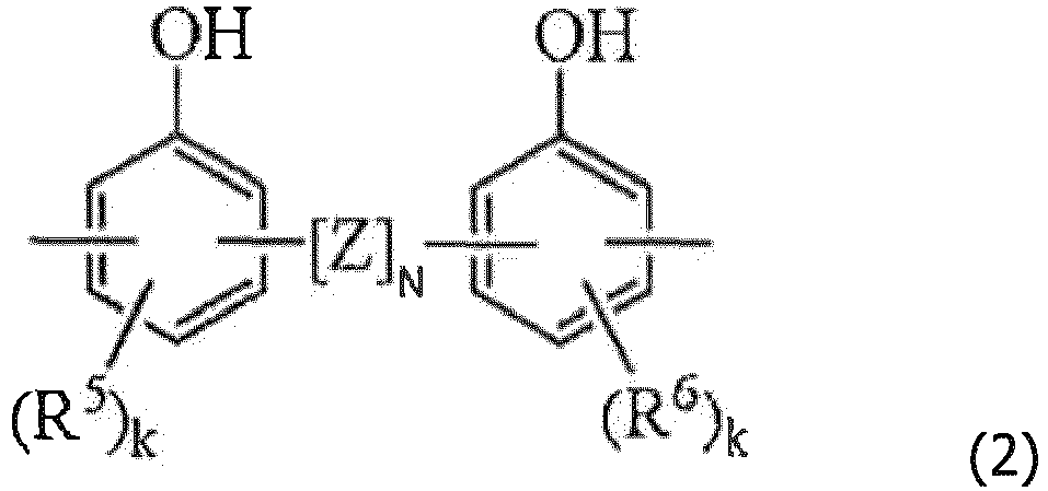

- Matériau adhésif provisoire pour un traitement de plaquette selon la revendication 12 ou 13, dans lequel la couche de polymère modifié par du siloxane thermodurcissable (B) est une couche durcie d'une composition contenant 100 parties en masse d'un polymère contenant une liaison siloxane ayant une unité de répétition représentée par la formule générale (3) suivante et un poids moléculaire moyen en poids de 3 000 à 500 000, et 0,1 à 50 parties en masse d'un ou plusieurs réticulants choisis dans le groupe constitué par un composé phénol ayant en moyenne deux groupes phénols ou plus par molécule et un composé époxyde ayant en moyenne deux groupes époxyde ou plus par molécule,


- Matériau adhésif provisoire pour un traitement de plaquette selon l'une quelconque des revendications 12 à 15, dans lequel la couche de polymère siloxane thermodurcissable (C) est une couche durcie d'une composition contenant :(C-1) un organopolysiloxane ayant deux groupes alcényle ou plus par molécule ;(C-2) un organohydrogénopolysiloxane ayant au moins deux atomes d'hydrogène liés à du silicium (groupes Si-H) par molécule, en une quantité telle qu'un rapport molaire du groupe Si-H dans le composant (C-2) au groupe alcényle dans le composant (C-1) varie de 0,3 à 10 ; et(C-3) un catalyseur à base de platine.
- Matériau adhésif provisoire pour un traitement de plaquette selon la revendication 16, dans lequel la couche de polymère siloxane thermodurcissable (C) contient en outre (C-4) un retardateur de réaction en une quantité de 0,1 à 10 parties en masse par rapport à 100 parties en masse d'un total du composant (C-1) et du composant (C-2).
- Matériau adhésif provisoire pour un traitement de plaquette selon l'une quelconque des revendications 12 à 17, dans lequel la couche de polymère modifié par du siloxane thermodurcissable (B) stratifiée sur la couche de polymère siloxane thermodurcissable (C) présente une force de pelage de 2 à 50 gf lorsque la couche de polymère (B) est pelée de manière interfaciale de la couche de polymère (C) après durcissement à chaud, la force de pelage étant mesurée par pelage à 180 ° en utilisant une pièce d'essai ayant une largeur de 25 mm lorsqu'elle est déterminée conformément aux indications fournies dans la description.
- Matériau adhésif provisoire pour un traitement de plaquette selon l'une quelconque des revendications 12 à 18, dans lequel une partie périphérique de la couche de polymère organopolysiloxane thermoplastique (A) est partiellement enlevée.
Applications Claiming Priority (2)
| Application Number | Priority Date | Filing Date | Title |
|---|---|---|---|
| JP2014014348 | 2014-01-29 | ||
| PCT/JP2015/000253 WO2015115060A1 (fr) | 2014-01-29 | 2015-01-21 | Pièce à usiner formant plaquette, matériau adhésif provisoire pour usinage de plaquette, et procédé de fabrication de plaquette mince |
Publications (3)
| Publication Number | Publication Date |
|---|---|
| EP3101681A1 EP3101681A1 (fr) | 2016-12-07 |
| EP3101681A4 EP3101681A4 (fr) | 2017-09-27 |
| EP3101681B1 true EP3101681B1 (fr) | 2020-03-25 |
Family
ID=53756647
Family Applications (1)
| Application Number | Title | Priority Date | Filing Date |
|---|---|---|---|
| EP15743005.9A Active EP3101681B1 (fr) | 2014-01-29 | 2015-01-21 | Pièce à usiner formant plaquette, matériau adhésif provisoire pour usinage de plaquette, et procédé de fabrication de plaquette mince |
Country Status (7)
| Country | Link |
|---|---|
| US (1) | US10106713B2 (fr) |
| EP (1) | EP3101681B1 (fr) |
| JP (1) | JP6130522B2 (fr) |
| KR (1) | KR102268248B1 (fr) |
| CN (1) | CN105960697B (fr) |
| TW (1) | TWI640436B (fr) |
| WO (1) | WO2015115060A1 (fr) |
Families Citing this family (23)
| Publication number | Priority date | Publication date | Assignee | Title |
|---|---|---|---|---|
| JP6023737B2 (ja) * | 2014-03-18 | 2016-11-09 | 信越化学工業株式会社 | ウエハ加工体、ウエハ加工用仮接着材、及び薄型ウエハの製造方法 |
| US10903106B2 (en) * | 2014-06-10 | 2021-01-26 | Nissan Chemical Industries, Ltd. | Layered body of temporary adhesive |
| JP6225894B2 (ja) * | 2014-12-24 | 2017-11-08 | 信越化学工業株式会社 | ウエハの仮接着方法及び薄型ウエハの製造方法 |
| JP6443241B2 (ja) * | 2015-06-30 | 2018-12-26 | 信越化学工業株式会社 | ウエハ加工用仮接着材、ウエハ加工体、及び薄型ウエハの製造方法 |
| JP6589766B2 (ja) * | 2015-08-18 | 2019-10-16 | 信越化学工業株式会社 | ウエハ加工用接着材、ウエハ積層体及び薄型ウエハの製造方法 |
| JP6610510B2 (ja) * | 2015-11-26 | 2019-11-27 | 信越化学工業株式会社 | ウエハ積層体及びその製造方法 |
| JP6463664B2 (ja) * | 2015-11-27 | 2019-02-06 | 信越化学工業株式会社 | ウエハ加工体及びウエハ加工方法 |
| US10074626B2 (en) * | 2016-06-06 | 2018-09-11 | Shin-Etsu Chemical Co., Ltd. | Wafer laminate and making method |
| JP6791086B2 (ja) * | 2016-10-11 | 2020-11-25 | 信越化学工業株式会社 | ウエハ積層体、その製造方法、及びウエハ積層用接着剤組成物 |
| KR102680736B1 (ko) * | 2016-12-14 | 2024-07-03 | 삼성전자주식회사 | 기판 가공 방법 및 접착층 세정 조성물 |
| WO2018216732A1 (fr) * | 2017-05-24 | 2018-11-29 | 日産化学株式会社 | Adhésif temporaire comprenant un polysiloxane modifié par époxy |
| JP6788549B2 (ja) * | 2017-06-05 | 2020-11-25 | 信越化学工業株式会社 | 基板加工用仮接着フィルムロール、薄型基板の製造方法 |
| US11472168B2 (en) * | 2017-11-01 | 2022-10-18 | Nissan Chemical Corporation | Laminated body including novolac resin as peeling layer |
| JP6998838B2 (ja) * | 2018-06-04 | 2022-01-18 | 信越化学工業株式会社 | 薄型基板の製造方法 |
| JP7035915B2 (ja) | 2018-09-03 | 2022-03-15 | 信越化学工業株式会社 | 薄型ウエハの製造方法 |
| JP2020131552A (ja) * | 2019-02-20 | 2020-08-31 | 株式会社東芝 | キャリアおよび半導体装置の製造方法 |
| JP7220119B2 (ja) | 2019-05-22 | 2023-02-09 | 信越化学工業株式会社 | 基板用仮接着剤の洗浄液、基板の洗浄方法および支持体または基板の洗浄方法 |
| WO2020235605A1 (fr) | 2019-05-22 | 2020-11-26 | 信越化学工業株式会社 | Composition d'agent de nettoyage, procédé de nettoyage de substrat, et procédé de nettoyage de corps de support ou substrat |
| JP7454922B2 (ja) * | 2019-07-11 | 2024-03-25 | 信越化学工業株式会社 | 基板加工用仮接着材料及び積層体の製造方法 |
| CN110591590B (zh) * | 2019-07-26 | 2021-10-01 | 四川羽玺新材料股份有限公司 | 一种低粘度耐高温保护膜的制备工艺 |
| JP7401247B2 (ja) * | 2019-10-08 | 2023-12-19 | 信越化学工業株式会社 | 硬化性組成物、その硬化物、及び半導体装置 |
| KR102680045B1 (ko) * | 2019-12-09 | 2024-06-28 | 쓰리엠 이노베이티브 프로퍼티즈 컴파니 | 접착 필름 |
| JP2024109166A (ja) | 2023-02-01 | 2024-08-14 | 信越化学工業株式会社 | 洗浄剤組成物及び洗浄方法 |
Family Cites Families (12)
| Publication number | Priority date | Publication date | Assignee | Title |
|---|---|---|---|---|
| CN1155562A (zh) * | 1995-10-11 | 1997-07-30 | 陶氏康宁公司 | 改进粘合性的可固化有机聚硅氧烷组合物 |
| US7534498B2 (en) | 2002-06-03 | 2009-05-19 | 3M Innovative Properties Company | Laminate body, method, and apparatus for manufacturing ultrathin substrate using the laminate body |
| JP4565804B2 (ja) | 2002-06-03 | 2010-10-20 | スリーエム イノベイティブ プロパティズ カンパニー | 被研削基材を含む積層体、その製造方法並びに積層体を用いた極薄基材の製造方法及びそのための装置 |
| JP4597508B2 (ja) | 2003-12-10 | 2010-12-15 | モメンティブ・パフォーマンス・マテリアルズ・ジャパン合同会社 | 半導体ペレットと半導体ペレット取付部材とを接合するためのシリコーン接着剤 |
| EP1854136A1 (fr) | 2005-03-01 | 2007-11-14 | Dow Corning Corporation | Procede de collage de tranche temporaire pour le traitement de semi-conducteurs |
| JP2006328104A (ja) | 2005-05-23 | 2006-12-07 | Jsr Corp | 接着剤組成物 |
| KR100941315B1 (ko) | 2007-12-17 | 2010-02-11 | 부산대학교 산학협력단 | 열경화성 접착제 조성물 및 이를 이용한 접착 필름 |
| JP5348147B2 (ja) | 2011-01-11 | 2013-11-20 | 信越化学工業株式会社 | 仮接着材組成物、及び薄型ウエハの製造方法 |
| JP6001568B2 (ja) | 2011-02-28 | 2016-10-05 | ダウ コーニング コーポレーションDow Corning Corporation | ウェハ接着システム、及びその接着並びに剥離方法 |
| JP5958262B2 (ja) * | 2011-10-28 | 2016-07-27 | 信越化学工業株式会社 | ウエハ加工体、ウエハ加工用部材、ウエハ加工用仮接着材、及び薄型ウエハの製造方法 |
| US8999817B2 (en) | 2012-02-28 | 2015-04-07 | Shin-Etsu Chemical Co., Ltd. | Wafer process body, wafer processing member, wafer processing temporary adhesive material, and method for manufacturing thin wafer |
| TWI534238B (zh) | 2012-04-24 | 2016-05-21 | 信越化學工業股份有限公司 | Wafer processing body, wafer processing member, temporary processing material for wafer processing, and manufacturing method of thin wafer |
-
2015
- 2015-01-21 EP EP15743005.9A patent/EP3101681B1/fr active Active
- 2015-01-21 CN CN201580006451.9A patent/CN105960697B/zh active Active
- 2015-01-21 US US15/110,576 patent/US10106713B2/en active Active
- 2015-01-21 WO PCT/JP2015/000253 patent/WO2015115060A1/fr not_active Ceased
- 2015-01-21 JP JP2015559809A patent/JP6130522B2/ja active Active
- 2015-01-21 KR KR1020167020763A patent/KR102268248B1/ko active Active
- 2015-01-28 TW TW104102908A patent/TWI640436B/zh active
Non-Patent Citations (1)
| Title |
|---|
| None * |
Also Published As
| Publication number | Publication date |
|---|---|
| TWI640436B (zh) | 2018-11-11 |
| KR20160114078A (ko) | 2016-10-04 |
| KR102268248B1 (ko) | 2021-06-24 |
| EP3101681A1 (fr) | 2016-12-07 |
| CN105960697A (zh) | 2016-09-21 |
| US10106713B2 (en) | 2018-10-23 |
| TW201542387A (zh) | 2015-11-16 |
| WO2015115060A1 (fr) | 2015-08-06 |
| EP3101681A4 (fr) | 2017-09-27 |
| JPWO2015115060A1 (ja) | 2017-03-23 |
| JP6130522B2 (ja) | 2017-05-17 |
| CN105960697B (zh) | 2019-06-11 |
| US20160326414A1 (en) | 2016-11-10 |
Similar Documents
| Publication | Publication Date | Title |
|---|---|---|
| US10106713B2 (en) | Wafer processing laminate, temporary adhesive material for wafer processing, and method for manufacturing thin wafer | |
| EP3121838B1 (fr) | Stratifié de traitement de plaquettes, matériau adhésif temporaire pour le traitement de plaquettes et procédé de fabrication de plaquette mince | |
| EP3037495B1 (fr) | Stratifié pour le traitement de tranches, matériau adhésif temporaire pour ledit traitement et procédé de fabrication d'une tranche mince | |
| EP3159924B1 (fr) | Stratifié pour le traitement de tranches, matériau adhésif temporaire pour ledit traitement et procédé de fabrication d'une tranche mince | |
| EP3000596B1 (fr) | Stratifié pour le traitement de tranches minces, matériau adhésif temporaire pour ledit traitement et procédé de fabrication d'une tranche mince | |
| EP3038148B1 (fr) | Procédé de collage temporaire de tranche et procédé de fabrication d'une tranche mince | |
| CN106318291B (zh) | 晶片加工用临时粘合构件、晶片加工用层叠体以及薄晶片的制造方法 | |
| EP2955211A1 (fr) | Matériau adhésif temporaire pour le traitement de tranches, stratifié de traitement de tranches et procédé de fabrication d'une tranche mince utilisant celui-ci | |
| EP3418340B1 (fr) | Rouleau de film adhésif temporaire pour traitement de substrats, procédé de fabrication de plaquettes minces | |
| US10854496B2 (en) | Circuit substrate processing laminate and method for processing circuit substrate | |
| EP3648147B1 (fr) | Procédé de fabrication d'un stratifié et procédé de fabrication d'un substrat |
Legal Events
| Date | Code | Title | Description |
|---|---|---|---|
| PUAI | Public reference made under article 153(3) epc to a published international application that has entered the european phase |
Free format text: ORIGINAL CODE: 0009012 |
|
| STAA | Information on the status of an ep patent application or granted ep patent |
Free format text: STATUS: REQUEST FOR EXAMINATION WAS MADE |
|
| 17P | Request for examination filed |
Effective date: 20160725 |
|
| AK | Designated contracting states |
Kind code of ref document: A1 Designated state(s): AL AT BE BG CH CY CZ DE DK EE ES FI FR GB GR HR HU IE IS IT LI LT LU LV MC MK MT NL NO PL PT RO RS SE SI SK SM TR |
|
| AX | Request for extension of the european patent |
Extension state: BA ME |
|
| DAX | Request for extension of the european patent (deleted) | ||
| A4 | Supplementary search report drawn up and despatched |
Effective date: 20170825 |
|
| RIC1 | Information provided on ipc code assigned before grant |
Ipc: C09J 183/04 20060101ALI20170821BHEP Ipc: H01L 21/304 20060101ALI20170821BHEP Ipc: B32B 7/06 20060101ALI20170821BHEP Ipc: H01L 21/02 20060101AFI20170821BHEP Ipc: B32B 27/00 20060101ALI20170821BHEP Ipc: C08L 83/04 20060101ALI20170821BHEP |
|
| STAA | Information on the status of an ep patent application or granted ep patent |
Free format text: STATUS: EXAMINATION IS IN PROGRESS |
|
| 17Q | First examination report despatched |
Effective date: 20181120 |
|
| GRAP | Despatch of communication of intention to grant a patent |
Free format text: ORIGINAL CODE: EPIDOSNIGR1 |
|
| STAA | Information on the status of an ep patent application or granted ep patent |
Free format text: STATUS: GRANT OF PATENT IS INTENDED |
|
| INTG | Intention to grant announced |
Effective date: 20191016 |
|
| GRAS | Grant fee paid |
Free format text: ORIGINAL CODE: EPIDOSNIGR3 |
|
| GRAA | (expected) grant |
Free format text: ORIGINAL CODE: 0009210 |
|
| STAA | Information on the status of an ep patent application or granted ep patent |
Free format text: STATUS: THE PATENT HAS BEEN GRANTED |
|
| AK | Designated contracting states |
Kind code of ref document: B1 Designated state(s): AL AT BE BG CH CY CZ DE DK EE ES FI FR GB GR HR HU IE IS IT LI LT LU LV MC MK MT NL NO PL PT RO RS SE SI SK SM TR |
|
| REG | Reference to a national code |
Ref country code: GB Ref legal event code: FG4D |
|
| RIN1 | Information on inventor provided before grant (corrected) |
Inventor name: TAGAMI, SHOHEI Inventor name: SUGO, MICHIHIRO |
|
| REG | Reference to a national code |
Ref country code: DE Ref legal event code: R096 Ref document number: 602015049392 Country of ref document: DE |
|
| REG | Reference to a national code |
Ref country code: AT Ref legal event code: REF Ref document number: 1249548 Country of ref document: AT Kind code of ref document: T Effective date: 20200415 Ref country code: IE Ref legal event code: FG4D |
|
| PG25 | Lapsed in a contracting state [announced via postgrant information from national office to epo] |
Ref country code: RS Free format text: LAPSE BECAUSE OF FAILURE TO SUBMIT A TRANSLATION OF THE DESCRIPTION OR TO PAY THE FEE WITHIN THE PRESCRIBED TIME-LIMIT Effective date: 20200325 Ref country code: FI Free format text: LAPSE BECAUSE OF FAILURE TO SUBMIT A TRANSLATION OF THE DESCRIPTION OR TO PAY THE FEE WITHIN THE PRESCRIBED TIME-LIMIT Effective date: 20200325 Ref country code: NO Free format text: LAPSE BECAUSE OF FAILURE TO SUBMIT A TRANSLATION OF THE DESCRIPTION OR TO PAY THE FEE WITHIN THE PRESCRIBED TIME-LIMIT Effective date: 20200625 |
|
| PG25 | Lapsed in a contracting state [announced via postgrant information from national office to epo] |
Ref country code: BG Free format text: LAPSE BECAUSE OF FAILURE TO SUBMIT A TRANSLATION OF THE DESCRIPTION OR TO PAY THE FEE WITHIN THE PRESCRIBED TIME-LIMIT Effective date: 20200625 Ref country code: GR Free format text: LAPSE BECAUSE OF FAILURE TO SUBMIT A TRANSLATION OF THE DESCRIPTION OR TO PAY THE FEE WITHIN THE PRESCRIBED TIME-LIMIT Effective date: 20200626 Ref country code: LV Free format text: LAPSE BECAUSE OF FAILURE TO SUBMIT A TRANSLATION OF THE DESCRIPTION OR TO PAY THE FEE WITHIN THE PRESCRIBED TIME-LIMIT Effective date: 20200325 Ref country code: SE Free format text: LAPSE BECAUSE OF FAILURE TO SUBMIT A TRANSLATION OF THE DESCRIPTION OR TO PAY THE FEE WITHIN THE PRESCRIBED TIME-LIMIT Effective date: 20200325 Ref country code: HR Free format text: LAPSE BECAUSE OF FAILURE TO SUBMIT A TRANSLATION OF THE DESCRIPTION OR TO PAY THE FEE WITHIN THE PRESCRIBED TIME-LIMIT Effective date: 20200325 |
|
| REG | Reference to a national code |
Ref country code: NL Ref legal event code: MP Effective date: 20200325 |
|
| REG | Reference to a national code |
Ref country code: LT Ref legal event code: MG4D |
|
| PG25 | Lapsed in a contracting state [announced via postgrant information from national office to epo] |
Ref country code: NL Free format text: LAPSE BECAUSE OF FAILURE TO SUBMIT A TRANSLATION OF THE DESCRIPTION OR TO PAY THE FEE WITHIN THE PRESCRIBED TIME-LIMIT Effective date: 20200325 |
|
| PG25 | Lapsed in a contracting state [announced via postgrant information from national office to epo] |
Ref country code: IS Free format text: LAPSE BECAUSE OF FAILURE TO SUBMIT A TRANSLATION OF THE DESCRIPTION OR TO PAY THE FEE WITHIN THE PRESCRIBED TIME-LIMIT Effective date: 20200725 Ref country code: SK Free format text: LAPSE BECAUSE OF FAILURE TO SUBMIT A TRANSLATION OF THE DESCRIPTION OR TO PAY THE FEE WITHIN THE PRESCRIBED TIME-LIMIT Effective date: 20200325 Ref country code: PT Free format text: LAPSE BECAUSE OF FAILURE TO SUBMIT A TRANSLATION OF THE DESCRIPTION OR TO PAY THE FEE WITHIN THE PRESCRIBED TIME-LIMIT Effective date: 20200818 Ref country code: LT Free format text: LAPSE BECAUSE OF FAILURE TO SUBMIT A TRANSLATION OF THE DESCRIPTION OR TO PAY THE FEE WITHIN THE PRESCRIBED TIME-LIMIT Effective date: 20200325 Ref country code: EE Free format text: LAPSE BECAUSE OF FAILURE TO SUBMIT A TRANSLATION OF THE DESCRIPTION OR TO PAY THE FEE WITHIN THE PRESCRIBED TIME-LIMIT Effective date: 20200325 Ref country code: SM Free format text: LAPSE BECAUSE OF FAILURE TO SUBMIT A TRANSLATION OF THE DESCRIPTION OR TO PAY THE FEE WITHIN THE PRESCRIBED TIME-LIMIT Effective date: 20200325 Ref country code: CZ Free format text: LAPSE BECAUSE OF FAILURE TO SUBMIT A TRANSLATION OF THE DESCRIPTION OR TO PAY THE FEE WITHIN THE PRESCRIBED TIME-LIMIT Effective date: 20200325 Ref country code: RO Free format text: LAPSE BECAUSE OF FAILURE TO SUBMIT A TRANSLATION OF THE DESCRIPTION OR TO PAY THE FEE WITHIN THE PRESCRIBED TIME-LIMIT Effective date: 20200325 |
|
| REG | Reference to a national code |
Ref country code: AT Ref legal event code: MK05 Ref document number: 1249548 Country of ref document: AT Kind code of ref document: T Effective date: 20200325 |
|
| REG | Reference to a national code |
Ref country code: DE Ref legal event code: R097 Ref document number: 602015049392 Country of ref document: DE |
|
| PG25 | Lapsed in a contracting state [announced via postgrant information from national office to epo] |
Ref country code: ES Free format text: LAPSE BECAUSE OF FAILURE TO SUBMIT A TRANSLATION OF THE DESCRIPTION OR TO PAY THE FEE WITHIN THE PRESCRIBED TIME-LIMIT Effective date: 20200325 Ref country code: DK Free format text: LAPSE BECAUSE OF FAILURE TO SUBMIT A TRANSLATION OF THE DESCRIPTION OR TO PAY THE FEE WITHIN THE PRESCRIBED TIME-LIMIT Effective date: 20200325 Ref country code: AT Free format text: LAPSE BECAUSE OF FAILURE TO SUBMIT A TRANSLATION OF THE DESCRIPTION OR TO PAY THE FEE WITHIN THE PRESCRIBED TIME-LIMIT Effective date: 20200325 |
|
| PLBE | No opposition filed within time limit |
Free format text: ORIGINAL CODE: 0009261 |
|
| STAA | Information on the status of an ep patent application or granted ep patent |
Free format text: STATUS: NO OPPOSITION FILED WITHIN TIME LIMIT |
|
| PG25 | Lapsed in a contracting state [announced via postgrant information from national office to epo] |
Ref country code: PL Free format text: LAPSE BECAUSE OF FAILURE TO SUBMIT A TRANSLATION OF THE DESCRIPTION OR TO PAY THE FEE WITHIN THE PRESCRIBED TIME-LIMIT Effective date: 20200325 |
|
| 26N | No opposition filed |
Effective date: 20210112 |
|
| PG25 | Lapsed in a contracting state [announced via postgrant information from national office to epo] |
Ref country code: SI Free format text: LAPSE BECAUSE OF FAILURE TO SUBMIT A TRANSLATION OF THE DESCRIPTION OR TO PAY THE FEE WITHIN THE PRESCRIBED TIME-LIMIT Effective date: 20200325 |
|
| PG25 | Lapsed in a contracting state [announced via postgrant information from national office to epo] |
Ref country code: MC Free format text: LAPSE BECAUSE OF FAILURE TO SUBMIT A TRANSLATION OF THE DESCRIPTION OR TO PAY THE FEE WITHIN THE PRESCRIBED TIME-LIMIT Effective date: 20200325 |
|
| REG | Reference to a national code |
Ref country code: CH Ref legal event code: PL |
|
| GBPC | Gb: european patent ceased through non-payment of renewal fee |
Effective date: 20210121 |
|
| PG25 | Lapsed in a contracting state [announced via postgrant information from national office to epo] |
Ref country code: LU Free format text: LAPSE BECAUSE OF NON-PAYMENT OF DUE FEES Effective date: 20210121 |
|
| REG | Reference to a national code |
Ref country code: BE Ref legal event code: MM Effective date: 20210131 |
|
| PG25 | Lapsed in a contracting state [announced via postgrant information from national office to epo] |
Ref country code: LI Free format text: LAPSE BECAUSE OF NON-PAYMENT OF DUE FEES Effective date: 20210131 Ref country code: GB Free format text: LAPSE BECAUSE OF NON-PAYMENT OF DUE FEES Effective date: 20210121 Ref country code: CH Free format text: LAPSE BECAUSE OF NON-PAYMENT OF DUE FEES Effective date: 20210131 |
|
| PG25 | Lapsed in a contracting state [announced via postgrant information from national office to epo] |
Ref country code: IE Free format text: LAPSE BECAUSE OF NON-PAYMENT OF DUE FEES Effective date: 20210121 |
|
| PG25 | Lapsed in a contracting state [announced via postgrant information from national office to epo] |
Ref country code: BE Free format text: LAPSE BECAUSE OF NON-PAYMENT OF DUE FEES Effective date: 20210131 |
|
| PG25 | Lapsed in a contracting state [announced via postgrant information from national office to epo] |
Ref country code: HU Free format text: LAPSE BECAUSE OF FAILURE TO SUBMIT A TRANSLATION OF THE DESCRIPTION OR TO PAY THE FEE WITHIN THE PRESCRIBED TIME-LIMIT; INVALID AB INITIO Effective date: 20150121 |
|
| PG25 | Lapsed in a contracting state [announced via postgrant information from national office to epo] |
Ref country code: CY Free format text: LAPSE BECAUSE OF FAILURE TO SUBMIT A TRANSLATION OF THE DESCRIPTION OR TO PAY THE FEE WITHIN THE PRESCRIBED TIME-LIMIT Effective date: 20200325 |
|
| PG25 | Lapsed in a contracting state [announced via postgrant information from national office to epo] |
Ref country code: MK Free format text: LAPSE BECAUSE OF FAILURE TO SUBMIT A TRANSLATION OF THE DESCRIPTION OR TO PAY THE FEE WITHIN THE PRESCRIBED TIME-LIMIT Effective date: 20200325 |
|
| PG25 | Lapsed in a contracting state [announced via postgrant information from national office to epo] |
Ref country code: MT Free format text: LAPSE BECAUSE OF FAILURE TO SUBMIT A TRANSLATION OF THE DESCRIPTION OR TO PAY THE FEE WITHIN THE PRESCRIBED TIME-LIMIT Effective date: 20200325 |
|
| REG | Reference to a national code |
Ref country code: DE Ref legal event code: R079 Ref document number: 602015049392 Country of ref document: DE Free format text: PREVIOUS MAIN CLASS: H01L0021020000 Ipc: H10P0095000000 |
|
| PG25 | Lapsed in a contracting state [announced via postgrant information from national office to epo] |
Ref country code: TR Free format text: LAPSE BECAUSE OF FAILURE TO SUBMIT A TRANSLATION OF THE DESCRIPTION OR TO PAY THE FEE WITHIN THE PRESCRIBED TIME-LIMIT Effective date: 20200325 |
|
| PGFP | Annual fee paid to national office [announced via postgrant information from national office to epo] |
Ref country code: FR Payment date: 20251128 Year of fee payment: 12 |
|
| PGFP | Annual fee paid to national office [announced via postgrant information from national office to epo] |
Ref country code: DE Payment date: 20251203 Year of fee payment: 12 |
|
| PGFP | Annual fee paid to national office [announced via postgrant information from national office to epo] |
Ref country code: IT Payment date: 20251219 Year of fee payment: 12 |