EP3101800B1 - System zur parallelen ansteuerung von wechselrichtern - Google Patents
System zur parallelen ansteuerung von wechselrichtern Download PDFInfo
- Publication number
- EP3101800B1 EP3101800B1 EP16169573.9A EP16169573A EP3101800B1 EP 3101800 B1 EP3101800 B1 EP 3101800B1 EP 16169573 A EP16169573 A EP 16169573A EP 3101800 B1 EP3101800 B1 EP 3101800B1
- Authority
- EP
- European Patent Office
- Prior art keywords
- output
- value
- inverters
- current
- phase
- Prior art date
- Legal status (The legal status is an assumption and is not a legal conclusion. Google has not performed a legal analysis and makes no representation as to the accuracy of the status listed.)
- Active
Links
Images


Classifications
-
- H—ELECTRICITY
- H02—GENERATION; CONVERSION OR DISTRIBUTION OF ELECTRIC POWER
- H02M—APPARATUS FOR CONVERSION BETWEEN AC AND AC, BETWEEN AC AND DC, OR BETWEEN DC AND DC, AND FOR USE WITH MAINS OR SIMILAR POWER SUPPLY SYSTEMS; CONVERSION OF DC OR AC INPUT POWER INTO SURGE OUTPUT POWER; CONTROL OR REGULATION THEREOF
- H02M7/00—Conversion of AC power input into DC power output; Conversion of DC power input into AC power output
- H02M7/42—Conversion of DC power input into AC power output without possibility of reversal
- H02M7/44—Conversion of DC power input into AC power output without possibility of reversal by static converters
- H02M7/48—Conversion of DC power input into AC power output without possibility of reversal by static converters using discharge tubes with control electrode or semiconductor devices with control electrode
-
- H—ELECTRICITY
- H02—GENERATION; CONVERSION OR DISTRIBUTION OF ELECTRIC POWER
- H02M—APPARATUS FOR CONVERSION BETWEEN AC AND AC, BETWEEN AC AND DC, OR BETWEEN DC AND DC, AND FOR USE WITH MAINS OR SIMILAR POWER SUPPLY SYSTEMS; CONVERSION OF DC OR AC INPUT POWER INTO SURGE OUTPUT POWER; CONTROL OR REGULATION THEREOF
- H02M7/00—Conversion of AC power input into DC power output; Conversion of DC power input into AC power output
- H02M7/42—Conversion of DC power input into AC power output without possibility of reversal
- H02M7/44—Conversion of DC power input into AC power output without possibility of reversal by static converters
- H02M7/48—Conversion of DC power input into AC power output without possibility of reversal by static converters using discharge tubes with control electrode or semiconductor devices with control electrode
- H02M7/493—Conversion of DC power input into AC power output without possibility of reversal by static converters using discharge tubes with control electrode or semiconductor devices with control electrode the static converters being arranged for operation in parallel
-
- H—ELECTRICITY
- H02—GENERATION; CONVERSION OR DISTRIBUTION OF ELECTRIC POWER
- H02M—APPARATUS FOR CONVERSION BETWEEN AC AND AC, BETWEEN AC AND DC, OR BETWEEN DC AND DC, AND FOR USE WITH MAINS OR SIMILAR POWER SUPPLY SYSTEMS; CONVERSION OF DC OR AC INPUT POWER INTO SURGE OUTPUT POWER; CONTROL OR REGULATION THEREOF
- H02M1/00—Details of apparatus for conversion
- H02M1/08—Circuits specially adapted for the generation of control voltages for semiconductor devices incorporated in static converters
-
- H—ELECTRICITY
- H02—GENERATION; CONVERSION OR DISTRIBUTION OF ELECTRIC POWER
- H02M—APPARATUS FOR CONVERSION BETWEEN AC AND AC, BETWEEN AC AND DC, OR BETWEEN DC AND DC, AND FOR USE WITH MAINS OR SIMILAR POWER SUPPLY SYSTEMS; CONVERSION OF DC OR AC INPUT POWER INTO SURGE OUTPUT POWER; CONTROL OR REGULATION THEREOF
- H02M7/00—Conversion of AC power input into DC power output; Conversion of DC power input into AC power output
- H02M7/42—Conversion of DC power input into AC power output without possibility of reversal
- H02M7/44—Conversion of DC power input into AC power output without possibility of reversal by static converters
-
- H—ELECTRICITY
- H02—GENERATION; CONVERSION OR DISTRIBUTION OF ELECTRIC POWER
- H02M—APPARATUS FOR CONVERSION BETWEEN AC AND AC, BETWEEN AC AND DC, OR BETWEEN DC AND DC, AND FOR USE WITH MAINS OR SIMILAR POWER SUPPLY SYSTEMS; CONVERSION OF DC OR AC INPUT POWER INTO SURGE OUTPUT POWER; CONTROL OR REGULATION THEREOF
- H02M7/00—Conversion of AC power input into DC power output; Conversion of DC power input into AC power output
- H02M7/42—Conversion of DC power input into AC power output without possibility of reversal
- H02M7/44—Conversion of DC power input into AC power output without possibility of reversal by static converters
- H02M7/48—Conversion of DC power input into AC power output without possibility of reversal by static converters using discharge tubes with control electrode or semiconductor devices with control electrode
- H02M7/53—Conversion of DC power input into AC power output without possibility of reversal by static converters using discharge tubes with control electrode or semiconductor devices with control electrode using devices of a triode or transistor type requiring continuous application of a control signal
- H02M7/537—Conversion of DC power input into AC power output without possibility of reversal by static converters using discharge tubes with control electrode or semiconductor devices with control electrode using devices of a triode or transistor type requiring continuous application of a control signal using semiconductor devices only, e.g. single switched pulse inverters
- H02M7/5387—Conversion of DC power input into AC power output without possibility of reversal by static converters using discharge tubes with control electrode or semiconductor devices with control electrode using devices of a triode or transistor type requiring continuous application of a control signal using semiconductor devices only, e.g. single switched pulse inverters in a bridge configuration
- H02M7/53871—Conversion of DC power input into AC power output without possibility of reversal by static converters using discharge tubes with control electrode or semiconductor devices with control electrode using devices of a triode or transistor type requiring continuous application of a control signal using semiconductor devices only, e.g. single switched pulse inverters in a bridge configuration with automatic control of output voltage or current
-
- H—ELECTRICITY
- H02—GENERATION; CONVERSION OR DISTRIBUTION OF ELECTRIC POWER
- H02M—APPARATUS FOR CONVERSION BETWEEN AC AND AC, BETWEEN AC AND DC, OR BETWEEN DC AND DC, AND FOR USE WITH MAINS OR SIMILAR POWER SUPPLY SYSTEMS; CONVERSION OF DC OR AC INPUT POWER INTO SURGE OUTPUT POWER; CONTROL OR REGULATION THEREOF
- H02M1/00—Details of apparatus for conversion
- H02M1/0003—Details of control, feedback or regulation circuits
- H02M1/0025—Arrangements for modifying reference values, feedback values or error values in the control loop of a converter
-
- H—ELECTRICITY
- H02—GENERATION; CONVERSION OR DISTRIBUTION OF ELECTRIC POWER
- H02P—CONTROL OR REGULATION OF ELECTRIC MOTORS, ELECTRIC GENERATORS OR DYNAMO-ELECTRIC CONVERTERS; CONTROLLING TRANSFORMERS, REACTORS OR CHOKE COILS
- H02P27/00—Arrangements or methods for the control of AC motors characterised by the kind of supply voltage
- H02P27/04—Arrangements or methods for the control of AC motors characterised by the kind of supply voltage using variable-frequency supply voltage, e.g. inverter or converter supply voltage
- H02P27/06—Arrangements or methods for the control of AC motors characterised by the kind of supply voltage using variable-frequency supply voltage, e.g. inverter or converter supply voltage using DC to AC converters or inverters
Definitions
- the present disclosure relates to a system for driving inverters in parallel, and more particularly to a system for driving inverters in parallel, in which a plurality of inverters are driven in parallel, to improve operation efficiency by correcting output current unbalance between inverters in the system.
- inverters which have a capacity higher than a given value are conventionally designed in a method for driving a plurality of inverters with a capacity smaller than a design capacity in parallel.
- Driving a plurality of inverters in parallel may be controlled in various methods.
- the most common method among the methods is to install a single master controller and a plurality of slave controllers to control the whole system through communication between them.
- KR 101361940 B1 discloses a prior art system for driving inverters in parallel by creating control signals for a slave controller to control inverters corresponding to the slave controller.
- the system comprises a single master controller, a plurality of slave controllers, a plurality of inverters and a control signal creation unit that is configured to create the control signals for the slave controllers.
- EP 2 874 302, A2 discloses another prior art solution, applicable to driving inverters in parallel, wherein a single master controller and a plurality of slave controllers are configured in a system for driving inverters.
- output current unbalance may occur between the inverters, which may be caused by different variables, for example, time differences that may occur by communication between the master controller and the slave controllers, the difference in power semiconductor features for the respective inverters, and time differences that occur between power semiconductor driving circuits installed in each inverter.
- FIG. 1 is an exemplary graph illustrating the state of inverter output current unbalance in a conventional system for driving inverters in parallel.
- FIG. 1 a small phase difference is shown among output currents Iu1, Iu2 and IuN of the N inverters. Because of such a difference, the sum of each inverter output does not match the whole system output in a system for driving inverters in parallel. For example, when designing power supply of 600kW with three inverters, it is essential to design power supply by connecting three inverters of a capacity even bigger than 200kW in parallel for safety reasons.
- Ptot total output power
- K is a derating factor, 0 ⁇ K ⁇ 1 (in inverse proportion to the number N of inverters connected in parallel
- Pinv is the capacity of each inverter connected in parallel. Therefore, there is a need to provide a new method for designing and operating a more efficient system by correcting the aforementioned output current unbalance of inverters driven in parallel.
- the present disclosure provides a system for driving inverters in parallel, in which a plurality of inverters are driven in parallel, for improving operation efficiency by correcting output current unbalance among the inverters in the system for driving the inverters in parallel, [insert page 3a]
- a system according to the invention is defined in claim 1.
- the proportional-integral controller is configured to find the sum of a value by multiplying the output values of the input adder by a proportional factor K p , and a value by multiplying an integrating factor K i by the integrated value of the output values of the input adder.
- the limiter is configured to output the output values of the current proportioning unit when the output values of the current proportioning unit lie between an upper limit value and a lower limit value predetermined by the limiter; configured to output the upper limit value predetermined by the limiter when the output values of the current proportioning unit are greater than the upper limit value; and configured to output the lower limit value predetermined by the limiter when the output values of the current proportioning unit are smaller than the lower limit value.
- the output adder is configured to find the sum of the pulse width values of the 3-phase output currents of each of the inverters and the output values of the limiter.
- the system for driving inverters in parallel enables each inverter which is a component of the system to output balanced current each other. This contributes to providing the effect of efficient design and operation of the system for driving inverters in parallel, configured by connecting a plurality of inverters.
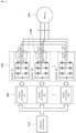
- FIG. 2 illustrates the configuration of a conventional system for driving inverters in parallel.
- the conventional system for driving inverters in parallel includes a single master controller 210, N slave controllers 220, N inverters 230 connected to each of the slave controllers 220, a 3-phase inductor 235 for attenuating output current waveform distortion of each inverter, and a motor 240 driven by driving the N inverters 230 in parallel.
- a 3-phase inductor 235 for attenuating output current waveform distortion of each inverter
- a motor 240 driven by driving the N inverters 230 in parallel.
- output power of each inverter is in charge of 1/N the power applied to the motor 240. Therefore, it is possible to drive a motor of large capacity by driving a plurality of inverters of small capacity in parallel.
- the current component of 3-phases u, v and w output from each inverter 230 is integrated to form the total current Iu, Iv and Iw.
- the current component of 3-phases u, v and w output from each inverter 230 is integrated to form the total current Iu, Iv and Iw.
- Iu component while total Iu is determined by the sum of the total current Iu1 of the inverter #1, the total current Iu2 of the inverter #2..., and the total current IuN of the inverter #N, each of the total currents Iu1, Iu2..., and IuN is not able to form its waveform which accurately matches as shown in FIG. 1 .
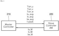
- FIG. 3 illustrates the concept of communication information between the master controller and the slave controllers shown in FIG. 2 .
- exemplary information sent from the master controller 210 to the slave controller 220 includes pulse width information Ton,u/ Ton,v/ Ton,w of 3-phase current, average value information Iu,avg/ Iv,avg/ Iw,avg of inverter output current, and average peak value information Ipeak of the current.
- exemplary information sent from the slave controller 220 to the master controller 210 includes 3-phase output current value information Iu,M/ Iv,M/ Iw,M for the inverter #M.
- control signal creation unit installed in the system of the present disclosure for driving inverters in parallel is described for controlling output signals of each of the slave controller 220 by creating compensating signals for controlling the output current of each phase to be balanced between the inverters being driven in parallel by using just the aforementioned information sent between the master controller 210 and the slave controller 220.
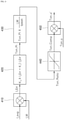
- FIG. 4 illustrates the configuration of a control signal creation unit installed in a system for driving inverters in parallel in accordance with an embodiment of the present disclosure.
- the control signal creation unit of the system for driving inverters in parallel includes an input adder 410, a proportional-integral controller 420, a current proportioning unit 430, a limiter 440, and an output adder 450.
- the proportional-integral controller 420 yields the output value Ton,Pi which is the sum of a value obtained by multiplying the output value I u ,Err of the input adder 410 by the proportional factor K p and a value obtained by multiplying the integral value of output value I u ,Err of the input adder 410 by the integrating factor K i .
- the current proportioning unit 430 performs a proportioning process, which is to differentiate the compensation range in consideration of each current phase, on the output value Ton,Pi of the proportional-integral controller 420, and the following Equation 4 is for the process.
- Ton , Ratio Ton , Pi ⁇ I u , M / Ipeak
- the output value Ton,Ratio of the current proportioning unit 430 is obtained by multiplying the output value Ton,Pi of the proportional-integral controller 420 by the value obtained by dividing the U-phase output current value I u ,M of the #M inverter by the average current peak value Ipeak.
- the U-phase output current value I u ,M information of the #M inverter can be obtained from the slave controller, and the average current peak value Ipeak information can be obtained from the master controller as described above.
- the limiter 440 performs an limiting process on the output value Ton,Ratio of the current proportioning unit 430 to limit the difference between the 3-phase output current value of a concerned inverter and the average 3-phase output current value. That is, if the difference between the U-phase output current value I u ,M of the #M inverter and the average U-phase output current value I u ,avg is too big, burning damage may occur in the inverter. Therefore, a limiting value is given to avoid the two values to be different by more than a given level to prevent the burning damage in the inverter.
- the operation by the limiter 440 contributes to obtaining the following compensating pulse width Ton,Comp.
- a compensating pulse width value Ton,Comp required for the U-phase output current value I u ,M of the #M inverter is determined as the aforementioned process result of the limiter 440.
- the U-phase output current pulse width Ton,u' of the #M inverter is finally determined by calculating the compensating pulse width values and the pulse width values of the 3-phase currents as described above. This process is carried out through the output adder 450 and the following Equation 6 is for the process.
- Ton , u ′ Ton , u + Ton , Comp
- the compensating pulse width value Ton,Cmp is calculated through the process of FIG. 4 and the above Equations for the U-phase output current pulse width Ton,u information sent from the master controller to the slave controller.
- Ton,Comp since a corrected U-phase output current pulse width Ton,u' information is calculated by the use of the value Ton,Comp, each of the slave controllers may control each of their corresponding inverters through the PWM control signals corresponding to the corrected information.
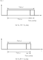
- FIG. 5 is an exemplary process of controlling output currents to illustrate FIG. 4 , and PWM output waveform of the slave controller for controlling the U-phase output current of the #M inverter.
- compensating each 3-phase output current value of any inverter as described above contributes to making all output current values of all inverters follow the average output current value thereof, and controlling output currents of the system for driving inverters in parallel to be balanced.
- FIG. 6 is a flow chart showing a method for controlling output currents of a system for driving inverters in parallel to be balanced in accordance with an embodiment of the present disclosure.
- the method for controlling output currents of the system for driving inverters in parallel to be balanced in accordance with an embodiment of the present disclosure includes an input adding process S610, a proportional-integral control process S620, a current proportioning process S630, a limiting process S640, and a output adding process S650.
- the input adding process S610 is an operation of finding a difference between the average output current value information of an inverter and the output current value information of the inverter, where a difference between the average value of each of 3-phase output currents of a plurality of inverters and each of the 3-phase output currents of the respective inverters is founded and outputted.
- the proportional-integral control process S620 is an operation of performing a proportional-integral control on the output values at the input adding process S610, where the proportional factor K p and the integrating factor K i , based on the derating factor K, is applied to the output values at the input adding process.
- the current proportioning process S630 is an operation of proportioning currents for differentiating a compensating range for each phase of current with respect to the output values at the proportional-integral control process S620. This process may be composed of multiplying the output values at the proportional-integral control process by the values obtained by dividing 3-phase output current values of the inverters by the average current peak value Ipeak of the inverters.
- the limiting process S640 is an operation of limiting the output values at the current proportioning process S630 in order to limit the difference between the 3-phase output current values and an average current value thereof. Specifically, when the output value at the current proportioning process S630 lies between any upper limit value and any lower limit value, the concerned output value is used as it is. However, when it is greater than the upper limit value, the upper limit value is applied, and the lower limit value is applied when it is smaller than the lower limit value, instead of the output value.
- the output adding process S650 is an operation of adding up the pulse width information of the 3-phase output currents to the output values at the limiting process S640. Through this process, all output current values of all inverters follow the average output current value of each output current value, which contributes to controlling output currents of the system for driving inverters in parallel to be balanced.
- the present disclosure may have the effect of controlling output currents of each phase to be balanced for each inverter just by sending and receiving information between a master controller and a slave controller in a system for driving N inverters in parallel.
- Controlling output currents to be balanced means that N inverters being driven in parallel are in charge of the same power. Therefore, applying the present disclosure contributes to providing various advantages including simplified design of a system for driving inverters in parallel, and furthermore to configuring an optimized efficient system.
Landscapes
- Engineering & Computer Science (AREA)
- Power Engineering (AREA)
- Inverter Devices (AREA)
Claims (3)
- System zum parallelen Antreiben von Wechselrichtern durch Erzeugen von Steuersignalen für eine Slave-Steuerung (220), um die Wechselrichter zu steuern, die der Slave-Steuerung (220) entsprechen, das System umfassend:eine Master-Steuerung (210);eine Vielzahl von Slave-Steuerungen (220);eine Vielzahl von Wechselrichtern (230), die von jeder der Slave-Steuerungen (220) entsprechend gesteuert werden; undeine Steuersignalerzeugungseinheit, die konfiguriert ist,Steuersignale für die Slave-Steuerungen (220) unter Verwendung von zwischen der Master-Steuerung (210) und den Slave-Steuerungen (220) gesendeten und empfangenen Daten zu erzeugen, um die Vielzahl von Wechselrichtern (230) in die Lage zu versetzen, ausgeglichene Ausgangsströme zu erzeugen, wobei für jeden Wechselrichter dieSteuersignalerzeugungseinheit für jede Phase umfasst:einen Eingangsaddierer (410), der konfiguriert ist,Differenzen zwischen dem Mittelwert (Iuavg) des Ausgangsstroms der ausgewählten Phase der Vielzahl von Wechselrichtern (230) zu finden, wobei der Mittelwert von der Master-Steuerung (210) und dem Ausgangsstromwert (IuM) der ausgewählten Phase der 3-Phasen-Ausgangsströme des ausgewählten Wechselrichters erhalten wird, wobei der Ausgangsstromwert von der Slave-Steuerung (220) des ausgewählten Wechselrichters (#M) erhalten wird;eine Proportional-Integral(PI)-Steuerung (420), die konfiguriert ist, eine Proportional-Integral-Steuerung auf Ausgangswerte des Eingangsaddierers (410) durchzuführen;eine Stromaufteilungseinheit (430), die konfiguriert ist,eine Aufteilung auf die Ausgangswerte der Proportional-Integral-Steuerung (420) durchzuführen, indem ein Ausgangswert der Proportional-Integral-Steuerung (420) mit einem Wert multipliziert wird, der durch Dividieren des Ausgangsstromwerts der ausgewählten Phase durch einen durchschnittlichen Stromspitzenwert (Ipeak) von der Master-Steuerung erhalten wird, um einen Kompensationsbereich für den ausgewählten Phasenstrom in Bezug auf die Ausgangswerte der Proportional-Integral(PI)-Steuerung (420) zu differenzieren;einen Begrenzer (440), der konfiguriert ist, eine Begrenzung auf die Ausgangswerte der Stromaufteilungseinheit (430) durchzuführen, um die Differenz zwischen den Durchschnittswerten der ausgewählten Phase der 3-phasigen Ausgangsströme und den Ausgangsstromwerten der ausgewählten Phase der 3-phasigen Ausgangsströme zu begrenzen; undeinen Ausgangsaddierer (450), der konfiguriert ist, Impulsbreiteninformationen zu der ausgewählten Phase der 3-phasigen Ausgangsströme zu Ausgangswerten des Begrenzers (440) zu addieren.
- System nach Anspruch 1, wobei die Proportional-Integral-Steuerung (420) konfiguriert ist, die Summe eines Wertes durch Multiplizieren der Eingangswerte des Eingangsaddierers (410) mit einem Proportionalfaktor Kp und eines Wertes durch Multiplizieren eines Integrationsfaktors Ki mit dem integrierten Wert der Ausgangswerte des Eingangsaddierers (410) zu finden.
- System nach Anspruch 1 oder 2, wobei der Begrenzer (440) konfiguriert ist, die Ausgangswerte der Stromaufteilungseinheit (430) auszugeben, wenn die Ausgangswerte der Stromaufteilungseinheit (430) zwischen einem oberen Grenzwert und einem unteren Grenzwert liegen, die durch den Begrenzer (440) vorbestimmt sind; konfiguriert, um den durch den Begrenzer (440) vorbestimmten oberen Grenzwert auszugeben, wenn die Ausgangswerte der Stromaufteilungseinheit (430) größer als der obere Grenzwert sind; und konfiguriert, um den durch den Begrenzer (440) vorbestimmten unteren Grenzwert auszugeben, wenn die Ausgangswerte der Stromaufteilungseinheit (430) kleiner als der untere Grenzwert sind.
Applications Claiming Priority (1)
| Application Number | Priority Date | Filing Date | Title |
|---|---|---|---|
| KR1020150077579A KR101695546B1 (ko) | 2015-06-01 | 2015-06-01 | 인버터 병렬 운전 시스템 |
Publications (2)
| Publication Number | Publication Date |
|---|---|
| EP3101800A1 EP3101800A1 (de) | 2016-12-07 |
| EP3101800B1 true EP3101800B1 (de) | 2022-02-23 |
Family
ID=56014837
Family Applications (1)
| Application Number | Title | Priority Date | Filing Date |
|---|---|---|---|
| EP16169573.9A Active EP3101800B1 (de) | 2015-06-01 | 2016-05-13 | System zur parallelen ansteuerung von wechselrichtern |
Country Status (6)
| Country | Link |
|---|---|
| US (1) | US9853566B2 (de) |
| EP (1) | EP3101800B1 (de) |
| JP (1) | JP6263575B2 (de) |
| KR (1) | KR101695546B1 (de) |
| CN (1) | CN106230286B (de) |
| ES (1) | ES2912980T3 (de) |
Families Citing this family (6)
| Publication number | Priority date | Publication date | Assignee | Title |
|---|---|---|---|---|
| DE102016107614A1 (de) * | 2016-04-25 | 2017-10-26 | Wobben Properties Gmbh | Wechselrichter und Verfahren zum Erzeugen eines Wechselstroms |
| CN108621862B (zh) * | 2017-03-15 | 2020-11-17 | 华为技术有限公司 | 电驱动控制系统、电动汽车和电驱动控制方法 |
| EP3518050B1 (de) * | 2018-01-26 | 2021-08-04 | Danfoss Mobile Electrification Oy | Verfahren und steuerungssystem zur steuerung von parallel betriebenen vorrichtungen |
| CN110277902B (zh) * | 2019-06-01 | 2021-02-09 | 上海沪工焊接集团股份有限公司 | 一种逆变电源的输入峰值电流检测和限制方法 |
| AT523577B1 (de) * | 2020-03-05 | 2024-06-15 | Avl List Gmbh | Maschinenumrichter und Verfahren zum Betrieb eines Maschinenumrichters |
| CN114244162B (zh) * | 2021-12-16 | 2024-08-16 | 深圳供电局有限公司 | 逆变器系统控制方法、装置、设备、存储介质和程序产品 |
Family Cites Families (18)
| Publication number | Priority date | Publication date | Assignee | Title |
|---|---|---|---|---|
| US5257180A (en) | 1991-04-22 | 1993-10-26 | Mitsubishi Denki Kabushiki Kaisha | Controlling system for parallel operation of AC output inverters with restrained cross currents |
| JP3185257B2 (ja) * | 1991-07-23 | 2001-07-09 | 株式会社明電舎 | 電力変換ユニットの並列運転装置 |
| JPH0884260A (ja) | 1994-09-12 | 1996-03-26 | Nippon Steel Corp | 2次元画像データの圧縮方式および伸長方式 |
| JPH08331854A (ja) * | 1995-06-02 | 1996-12-13 | Toyo Electric Mfg Co Ltd | 複数台インバ−タ並列運転装置 |
| JPH09331682A (ja) | 1996-06-12 | 1997-12-22 | Meidensha Corp | 電力変換器 |
| JP4923918B2 (ja) | 2006-09-28 | 2012-04-25 | 株式会社明電舎 | インバータ装置の並列運転装置 |
| KR20090096841A (ko) * | 2008-03-10 | 2009-09-15 | 엘에스산전 주식회사 | 인버터의 병렬 운전에서 전류균형 제어장치 |
| US9106201B1 (en) * | 2010-06-23 | 2015-08-11 | Volterra Semiconductor Corporation | Systems and methods for DC-to-DC converter control |
| JP5867032B2 (ja) | 2011-12-02 | 2016-02-24 | 富士電機株式会社 | 並列インバータ装置 |
| US9891679B2 (en) * | 2011-12-22 | 2018-02-13 | Astec International Limited | Single phase redundant power supply systems for reducing phase current imbalances |
| CN103378742B (zh) * | 2012-04-18 | 2016-02-03 | 台达电子企业管理(上海)有限公司 | 变流器系统及其控制方法 |
| JP5891940B2 (ja) | 2012-05-17 | 2016-03-23 | 富士電機株式会社 | 3レベルユニットインバータ |
| KR101361940B1 (ko) * | 2013-02-18 | 2014-02-12 | 엘에스산전 주식회사 | 병렬 운전 인버터 시스템의 슬레이브 제어기 |
| FR3013528B1 (fr) * | 2013-11-19 | 2016-01-01 | Valeo Equip Electr Moteur | Boucle de regulation porportionnelle integrale pour un dispositif regulateur numerique de machine electrique tournante a excitation de vehicule automobile |
| KR101491933B1 (ko) | 2013-11-19 | 2015-02-09 | 엘에스산전 주식회사 | 병렬 인버터 제어 장치 |
| US20150145462A1 (en) * | 2013-11-25 | 2015-05-28 | Rockwell Automation Technologies, Inc. | Method and apparatus for current auto balancing for parallel converter systems |
| US9837921B2 (en) * | 2014-09-08 | 2017-12-05 | Infineon Technologies Austria Ag | Multi-cell power conversion method and multi-cell power converter |
| CN105990999A (zh) * | 2015-01-27 | 2016-10-05 | 台达电子工业股份有限公司 | 电源供应装置及其控制方法 |
-
2015
- 2015-06-01 KR KR1020150077579A patent/KR101695546B1/ko active Active
-
2016
- 2016-05-13 ES ES16169573T patent/ES2912980T3/es active Active
- 2016-05-13 EP EP16169573.9A patent/EP3101800B1/de active Active
- 2016-05-26 US US15/166,172 patent/US9853566B2/en active Active
- 2016-05-31 CN CN201610374967.5A patent/CN106230286B/zh active Active
- 2016-06-01 JP JP2016109913A patent/JP6263575B2/ja active Active
Also Published As
| Publication number | Publication date |
|---|---|
| ES2912980T3 (es) | 2022-05-30 |
| KR20160141937A (ko) | 2016-12-12 |
| KR101695546B1 (ko) | 2017-01-12 |
| CN106230286A (zh) | 2016-12-14 |
| EP3101800A1 (de) | 2016-12-07 |
| CN106230286B (zh) | 2018-11-20 |
| JP6263575B2 (ja) | 2018-01-17 |
| US9853566B2 (en) | 2017-12-26 |
| JP2016226282A (ja) | 2016-12-28 |
| US20160352250A1 (en) | 2016-12-01 |
Similar Documents
| Publication | Publication Date | Title |
|---|---|---|
| EP3101800A1 (de) | System zur parallelen ansteuerung von wechselrichtern | |
| EP2876797A2 (de) | Verfahren und Vorrichtung für automatischen Stromausgleich für Parallelwandleranlagen | |
| EP2874302B1 (de) | Vorrichtung zur Steuerung parallelgeschalteter Wechselrichter | |
| US11146179B2 (en) | Power conversion device, power conversion system, and power conversion method | |
| US10374531B2 (en) | Motor control device and electric power steering system using said motor drive circuit | |
| JP2016063559A (ja) | モータ制御装置 | |
| EP3713075A1 (de) | Leistungswandlungssystem | |
| US20240106351A1 (en) | Multi-inverter parallel system and method for controlling grid connection of inverter | |
| US20190074791A1 (en) | Inverter control device | |
| US11374505B2 (en) | Inverter device for performing a power conversion operation to convert DC power to AC power | |
| CN106575932B (zh) | 电动机控制装置、电动机控制方法以及电动机控制系统 | |
| JP2015201956A (ja) | ベクトル制御装置、それを組み込んだインバータ及びそれを組み込んだインバータとモータとのセット装置 | |
| EP4109738A1 (de) | System und verfahren zur bahnformung für machbare bewegungsbefehle | |
| KR101361940B1 (ko) | 병렬 운전 인버터 시스템의 슬레이브 제어기 | |
| JP6553991B2 (ja) | モータ制御装置 | |
| EP4224697A1 (de) | Verfahren, computerprogramm und steuergerät zur steuerung eines elektrischen wandlers, elektrischer wandler und computerlesbares medium | |
| CN118435485A (zh) | 用于控制并联连接的功率转换器的方法和控制系统 | |
| CN111869089B (zh) | 用于运行多相电机的方法和设备 | |
| EP4228143A1 (de) | Verfahren, computerprogramm und steuergerät zur steuerung eines elektrischen wandlers, elektrischer wandler und computerlesbares medium | |
| CN113411027B (zh) | 一种开关频率的控制装置、电机及其开关频率的控制方法 | |
| JP5416337B2 (ja) | 電動機制御装置 | |
| KR20250101408A (ko) | 모터 제어 방법 및 장치 | |
| CN104065086A (zh) | 一种用于静止无功发生装置的并联运行控制器及其控制方法 | |
| JP2020191754A (ja) | モータ駆動制御装置及びその制御方法 |
Legal Events
| Date | Code | Title | Description |
|---|---|---|---|
| PUAI | Public reference made under article 153(3) epc to a published international application that has entered the european phase |
Free format text: ORIGINAL CODE: 0009012 |
|
| STAA | Information on the status of an ep patent application or granted ep patent |
Free format text: STATUS: THE APPLICATION HAS BEEN PUBLISHED |
|
| AK | Designated contracting states |
Kind code of ref document: A1 Designated state(s): AL AT BE BG CH CY CZ DE DK EE ES FI FR GB GR HR HU IE IS IT LI LT LU LV MC MK MT NL NO PL PT RO RS SE SI SK SM TR |
|
| AX | Request for extension of the european patent |
Extension state: BA ME |
|
| STAA | Information on the status of an ep patent application or granted ep patent |
Free format text: STATUS: REQUEST FOR EXAMINATION WAS MADE |
|
| STAA | Information on the status of an ep patent application or granted ep patent |
Free format text: STATUS: EXAMINATION IS IN PROGRESS |
|
| 17P | Request for examination filed |
Effective date: 20170530 |
|
| RBV | Designated contracting states (corrected) |
Designated state(s): AL AT BE BG CH CY CZ DE DK EE ES FI FR GB GR HR HU IE IS IT LI LT LU LV MC MK MT NL NO PL PT RO RS SE SI SK SM TR |
|
| 17Q | First examination report despatched |
Effective date: 20170628 |
|
| GRAP | Despatch of communication of intention to grant a patent |
Free format text: ORIGINAL CODE: EPIDOSNIGR1 |
|
| STAA | Information on the status of an ep patent application or granted ep patent |
Free format text: STATUS: GRANT OF PATENT IS INTENDED |
|
| INTG | Intention to grant announced |
Effective date: 20210914 |
|
| GRAS | Grant fee paid |
Free format text: ORIGINAL CODE: EPIDOSNIGR3 |
|
| GRAA | (expected) grant |
Free format text: ORIGINAL CODE: 0009210 |
|
| STAA | Information on the status of an ep patent application or granted ep patent |
Free format text: STATUS: THE PATENT HAS BEEN GRANTED |
|
| AK | Designated contracting states |
Kind code of ref document: B1 Designated state(s): AL AT BE BG CH CY CZ DE DK EE ES FI FR GB GR HR HU IE IS IT LI LT LU LV MC MK MT NL NO PL PT RO RS SE SI SK SM TR |
|
| REG | Reference to a national code |
Ref country code: GB Ref legal event code: FG4D |
|
| REG | Reference to a national code |
Ref country code: CH Ref legal event code: EP |
|
| REG | Reference to a national code |
Ref country code: DE Ref legal event code: R096 Ref document number: 602016069293 Country of ref document: DE |
|
| REG | Reference to a national code |
Ref country code: AT Ref legal event code: REF Ref document number: 1471222 Country of ref document: AT Kind code of ref document: T Effective date: 20220315 |
|
| REG | Reference to a national code |
Ref country code: IE Ref legal event code: FG4D |
|
| REG | Reference to a national code |
Ref country code: ES Ref legal event code: FG2A Ref document number: 2912980 Country of ref document: ES Kind code of ref document: T3 Effective date: 20220530 |
|
| REG | Reference to a national code |
Ref country code: LT Ref legal event code: MG9D |
|
| REG | Reference to a national code |
Ref country code: NL Ref legal event code: MP Effective date: 20220223 |
|
| REG | Reference to a national code |
Ref country code: AT Ref legal event code: MK05 Ref document number: 1471222 Country of ref document: AT Kind code of ref document: T Effective date: 20220223 |
|
| PG25 | Lapsed in a contracting state [announced via postgrant information from national office to epo] |
Ref country code: SE Free format text: LAPSE BECAUSE OF FAILURE TO SUBMIT A TRANSLATION OF THE DESCRIPTION OR TO PAY THE FEE WITHIN THE PRESCRIBED TIME-LIMIT Effective date: 20220223 Ref country code: RS Free format text: LAPSE BECAUSE OF FAILURE TO SUBMIT A TRANSLATION OF THE DESCRIPTION OR TO PAY THE FEE WITHIN THE PRESCRIBED TIME-LIMIT Effective date: 20220223 Ref country code: PT Free format text: LAPSE BECAUSE OF FAILURE TO SUBMIT A TRANSLATION OF THE DESCRIPTION OR TO PAY THE FEE WITHIN THE PRESCRIBED TIME-LIMIT Effective date: 20220623 Ref country code: NO Free format text: LAPSE BECAUSE OF FAILURE TO SUBMIT A TRANSLATION OF THE DESCRIPTION OR TO PAY THE FEE WITHIN THE PRESCRIBED TIME-LIMIT Effective date: 20220523 Ref country code: NL Free format text: LAPSE BECAUSE OF FAILURE TO SUBMIT A TRANSLATION OF THE DESCRIPTION OR TO PAY THE FEE WITHIN THE PRESCRIBED TIME-LIMIT Effective date: 20220223 Ref country code: LT Free format text: LAPSE BECAUSE OF FAILURE TO SUBMIT A TRANSLATION OF THE DESCRIPTION OR TO PAY THE FEE WITHIN THE PRESCRIBED TIME-LIMIT Effective date: 20220223 Ref country code: HR Free format text: LAPSE BECAUSE OF FAILURE TO SUBMIT A TRANSLATION OF THE DESCRIPTION OR TO PAY THE FEE WITHIN THE PRESCRIBED TIME-LIMIT Effective date: 20220223 Ref country code: BG Free format text: LAPSE BECAUSE OF FAILURE TO SUBMIT A TRANSLATION OF THE DESCRIPTION OR TO PAY THE FEE WITHIN THE PRESCRIBED TIME-LIMIT Effective date: 20220523 |
|
| PG25 | Lapsed in a contracting state [announced via postgrant information from national office to epo] |
Ref country code: PL Free format text: LAPSE BECAUSE OF FAILURE TO SUBMIT A TRANSLATION OF THE DESCRIPTION OR TO PAY THE FEE WITHIN THE PRESCRIBED TIME-LIMIT Effective date: 20220223 Ref country code: LV Free format text: LAPSE BECAUSE OF FAILURE TO SUBMIT A TRANSLATION OF THE DESCRIPTION OR TO PAY THE FEE WITHIN THE PRESCRIBED TIME-LIMIT Effective date: 20220223 Ref country code: GR Free format text: LAPSE BECAUSE OF FAILURE TO SUBMIT A TRANSLATION OF THE DESCRIPTION OR TO PAY THE FEE WITHIN THE PRESCRIBED TIME-LIMIT Effective date: 20220524 Ref country code: FI Free format text: LAPSE BECAUSE OF FAILURE TO SUBMIT A TRANSLATION OF THE DESCRIPTION OR TO PAY THE FEE WITHIN THE PRESCRIBED TIME-LIMIT Effective date: 20220223 Ref country code: AT Free format text: LAPSE BECAUSE OF FAILURE TO SUBMIT A TRANSLATION OF THE DESCRIPTION OR TO PAY THE FEE WITHIN THE PRESCRIBED TIME-LIMIT Effective date: 20220223 |
|
| PG25 | Lapsed in a contracting state [announced via postgrant information from national office to epo] |
Ref country code: IS Free format text: LAPSE BECAUSE OF FAILURE TO SUBMIT A TRANSLATION OF THE DESCRIPTION OR TO PAY THE FEE WITHIN THE PRESCRIBED TIME-LIMIT Effective date: 20220623 |
|
| PG25 | Lapsed in a contracting state [announced via postgrant information from national office to epo] |
Ref country code: SM Free format text: LAPSE BECAUSE OF FAILURE TO SUBMIT A TRANSLATION OF THE DESCRIPTION OR TO PAY THE FEE WITHIN THE PRESCRIBED TIME-LIMIT Effective date: 20220223 Ref country code: SK Free format text: LAPSE BECAUSE OF FAILURE TO SUBMIT A TRANSLATION OF THE DESCRIPTION OR TO PAY THE FEE WITHIN THE PRESCRIBED TIME-LIMIT Effective date: 20220223 Ref country code: RO Free format text: LAPSE BECAUSE OF FAILURE TO SUBMIT A TRANSLATION OF THE DESCRIPTION OR TO PAY THE FEE WITHIN THE PRESCRIBED TIME-LIMIT Effective date: 20220223 Ref country code: EE Free format text: LAPSE BECAUSE OF FAILURE TO SUBMIT A TRANSLATION OF THE DESCRIPTION OR TO PAY THE FEE WITHIN THE PRESCRIBED TIME-LIMIT Effective date: 20220223 Ref country code: DK Free format text: LAPSE BECAUSE OF FAILURE TO SUBMIT A TRANSLATION OF THE DESCRIPTION OR TO PAY THE FEE WITHIN THE PRESCRIBED TIME-LIMIT Effective date: 20220223 Ref country code: CZ Free format text: LAPSE BECAUSE OF FAILURE TO SUBMIT A TRANSLATION OF THE DESCRIPTION OR TO PAY THE FEE WITHIN THE PRESCRIBED TIME-LIMIT Effective date: 20220223 |
|
| REG | Reference to a national code |
Ref country code: DE Ref legal event code: R097 Ref document number: 602016069293 Country of ref document: DE |
|
| PG25 | Lapsed in a contracting state [announced via postgrant information from national office to epo] |
Ref country code: AL Free format text: LAPSE BECAUSE OF FAILURE TO SUBMIT A TRANSLATION OF THE DESCRIPTION OR TO PAY THE FEE WITHIN THE PRESCRIBED TIME-LIMIT Effective date: 20220223 |
|
| PLBE | No opposition filed within time limit |
Free format text: ORIGINAL CODE: 0009261 |
|
| REG | Reference to a national code |
Ref country code: CH Ref legal event code: PL |
|
| STAA | Information on the status of an ep patent application or granted ep patent |
Free format text: STATUS: NO OPPOSITION FILED WITHIN TIME LIMIT |
|
| REG | Reference to a national code |
Ref country code: BE Ref legal event code: MM Effective date: 20220531 |
|
| PG25 | Lapsed in a contracting state [announced via postgrant information from national office to epo] |
Ref country code: MC Free format text: LAPSE BECAUSE OF FAILURE TO SUBMIT A TRANSLATION OF THE DESCRIPTION OR TO PAY THE FEE WITHIN THE PRESCRIBED TIME-LIMIT Effective date: 20220223 Ref country code: LU Free format text: LAPSE BECAUSE OF NON-PAYMENT OF DUE FEES Effective date: 20220513 Ref country code: LI Free format text: LAPSE BECAUSE OF NON-PAYMENT OF DUE FEES Effective date: 20220531 Ref country code: CH Free format text: LAPSE BECAUSE OF NON-PAYMENT OF DUE FEES Effective date: 20220531 |
|
| 26N | No opposition filed |
Effective date: 20221124 |
|
| PG25 | Lapsed in a contracting state [announced via postgrant information from national office to epo] |
Ref country code: SI Free format text: LAPSE BECAUSE OF FAILURE TO SUBMIT A TRANSLATION OF THE DESCRIPTION OR TO PAY THE FEE WITHIN THE PRESCRIBED TIME-LIMIT Effective date: 20220223 |
|
| PG25 | Lapsed in a contracting state [announced via postgrant information from national office to epo] |
Ref country code: IE Free format text: LAPSE BECAUSE OF NON-PAYMENT OF DUE FEES Effective date: 20220513 Ref country code: FR Free format text: LAPSE BECAUSE OF NON-PAYMENT OF DUE FEES Effective date: 20220531 |
|
| PG25 | Lapsed in a contracting state [announced via postgrant information from national office to epo] |
Ref country code: BE Free format text: LAPSE BECAUSE OF NON-PAYMENT OF DUE FEES Effective date: 20220531 |
|
| P01 | Opt-out of the competence of the unified patent court (upc) registered |
Effective date: 20230625 |
|
| PG25 | Lapsed in a contracting state [announced via postgrant information from national office to epo] |
Ref country code: HU Free format text: LAPSE BECAUSE OF FAILURE TO SUBMIT A TRANSLATION OF THE DESCRIPTION OR TO PAY THE FEE WITHIN THE PRESCRIBED TIME-LIMIT; INVALID AB INITIO Effective date: 20160513 |
|
| PG25 | Lapsed in a contracting state [announced via postgrant information from national office to epo] |
Ref country code: MK Free format text: LAPSE BECAUSE OF FAILURE TO SUBMIT A TRANSLATION OF THE DESCRIPTION OR TO PAY THE FEE WITHIN THE PRESCRIBED TIME-LIMIT Effective date: 20220223 Ref country code: CY Free format text: LAPSE BECAUSE OF FAILURE TO SUBMIT A TRANSLATION OF THE DESCRIPTION OR TO PAY THE FEE WITHIN THE PRESCRIBED TIME-LIMIT Effective date: 20220223 |
|
| PG25 | Lapsed in a contracting state [announced via postgrant information from national office to epo] |
Ref country code: TR Free format text: LAPSE BECAUSE OF FAILURE TO SUBMIT A TRANSLATION OF THE DESCRIPTION OR TO PAY THE FEE WITHIN THE PRESCRIBED TIME-LIMIT Effective date: 20220223 |
|
| PG25 | Lapsed in a contracting state [announced via postgrant information from national office to epo] |
Ref country code: MT Free format text: LAPSE BECAUSE OF FAILURE TO SUBMIT A TRANSLATION OF THE DESCRIPTION OR TO PAY THE FEE WITHIN THE PRESCRIBED TIME-LIMIT Effective date: 20220223 |
|
| PGFP | Annual fee paid to national office [announced via postgrant information from national office to epo] |
Ref country code: GB Payment date: 20260309 Year of fee payment: 11 |
|
| PGFP | Annual fee paid to national office [announced via postgrant information from national office to epo] |
Ref country code: IT Payment date: 20260306 Year of fee payment: 11 |
|
| PGFP | Annual fee paid to national office [announced via postgrant information from national office to epo] |
Ref country code: ES Payment date: 20260608 Year of fee payment: 11 |
|
| PGFP | Annual fee paid to national office [announced via postgrant information from national office to epo] |
Ref country code: DE Payment date: 20260305 Year of fee payment: 11 |