EP3101809A1 - Halbleiterelementansteuerungsvorrichtung leistungswandlervorrichtung damit - Google Patents
Halbleiterelementansteuerungsvorrichtung leistungswandlervorrichtung damit Download PDFInfo
- Publication number
- EP3101809A1 EP3101809A1 EP14881018.7A EP14881018A EP3101809A1 EP 3101809 A1 EP3101809 A1 EP 3101809A1 EP 14881018 A EP14881018 A EP 14881018A EP 3101809 A1 EP3101809 A1 EP 3101809A1
- Authority
- EP
- European Patent Office
- Prior art keywords
- layer
- semiconductor layer
- type
- semiconductor
- semiconductor element
- Prior art date
- Legal status (The legal status is an assumption and is not a legal conclusion. Google has not performed a legal analysis and makes no representation as to the accuracy of the status listed.)
- Withdrawn
Links
Images






Classifications
-
- H—ELECTRICITY
- H10—SEMICONDUCTOR DEVICES; ELECTRIC SOLID-STATE DEVICES NOT OTHERWISE PROVIDED FOR
- H10D—INORGANIC ELECTRIC SEMICONDUCTOR DEVICES
- H10D12/00—Bipolar devices controlled by the field effect, e.g. insulated-gate bipolar transistors [IGBT]
- H10D12/211—Gated diodes
-
- H—ELECTRICITY
- H02—GENERATION; CONVERSION OR DISTRIBUTION OF ELECTRIC POWER
- H02M—APPARATUS FOR CONVERSION BETWEEN AC AND AC, BETWEEN AC AND DC, OR BETWEEN DC AND DC, AND FOR USE WITH MAINS OR SIMILAR POWER SUPPLY SYSTEMS; CONVERSION OF DC OR AC INPUT POWER INTO SURGE OUTPUT POWER; CONTROL OR REGULATION THEREOF
- H02M7/00—Conversion of AC power input into DC power output; Conversion of DC power input into AC power output
- H02M7/003—Constructional details, e.g. physical layout, assembly, wiring or busbar connections
-
- H—ELECTRICITY
- H02—GENERATION; CONVERSION OR DISTRIBUTION OF ELECTRIC POWER
- H02M—APPARATUS FOR CONVERSION BETWEEN AC AND AC, BETWEEN AC AND DC, OR BETWEEN DC AND DC, AND FOR USE WITH MAINS OR SIMILAR POWER SUPPLY SYSTEMS; CONVERSION OF DC OR AC INPUT POWER INTO SURGE OUTPUT POWER; CONTROL OR REGULATION THEREOF
- H02M7/00—Conversion of AC power input into DC power output; Conversion of DC power input into AC power output
- H02M7/42—Conversion of DC power input into AC power output without possibility of reversal
- H02M7/44—Conversion of DC power input into AC power output without possibility of reversal by static converters
-
- H—ELECTRICITY
- H03—ELECTRONIC CIRCUITRY
- H03K—PULSE TECHNIQUE
- H03K17/00—Electronic switching or gating, i.e. not by contact-making and –breaking
- H03K17/16—Modifications for eliminating interference voltages or currents
- H03K17/161—Modifications for eliminating interference voltages or currents in field-effect transistor switches
- H03K17/162—Modifications for eliminating interference voltages or currents in field-effect transistor switches without feedback from the output circuit to the control circuit
-
- H—ELECTRICITY
- H03—ELECTRONIC CIRCUITRY
- H03K—PULSE TECHNIQUE
- H03K17/00—Electronic switching or gating, i.e. not by contact-making and –breaking
- H03K17/51—Electronic switching or gating, i.e. not by contact-making and –breaking characterised by the components used
- H03K17/74—Electronic switching or gating, i.e. not by contact-making and –breaking characterised by the components used by the use, as active elements, of diodes
-
- H—ELECTRICITY
- H10—SEMICONDUCTOR DEVICES; ELECTRIC SOLID-STATE DEVICES NOT OTHERWISE PROVIDED FOR
- H10D—INORGANIC ELECTRIC SEMICONDUCTOR DEVICES
- H10D12/00—Bipolar devices controlled by the field effect, e.g. insulated-gate bipolar transistors [IGBT]
- H10D12/411—Insulated-gate bipolar transistors [IGBT]
- H10D12/441—Vertical IGBTs
- H10D12/461—Vertical IGBTs having non-planar surfaces, e.g. having trenches, recesses or pillars in the surfaces of the emitter, base or collector regions
- H10D12/481—Vertical IGBTs having non-planar surfaces, e.g. having trenches, recesses or pillars in the surfaces of the emitter, base or collector regions having gate structures on slanted surfaces, on vertical surfaces, or in grooves, e.g. trench gate IGBTs
-
- H—ELECTRICITY
- H10—SEMICONDUCTOR DEVICES; ELECTRIC SOLID-STATE DEVICES NOT OTHERWISE PROVIDED FOR
- H10D—INORGANIC ELECTRIC SEMICONDUCTOR DEVICES
- H10D62/00—Semiconductor bodies, or regions thereof, of devices having potential barriers
- H10D62/10—Shapes, relative sizes or dispositions of the regions of the semiconductor bodies; Shapes of the semiconductor bodies
- H10D62/13—Semiconductor regions connected to electrodes carrying current to be rectified, amplified or switched, e.g. source or drain regions
- H10D62/141—Anode or cathode regions of thyristors; Collector or emitter regions of gated bipolar-mode devices, e.g. of IGBTs
-
- H—ELECTRICITY
- H10—SEMICONDUCTOR DEVICES; ELECTRIC SOLID-STATE DEVICES NOT OTHERWISE PROVIDED FOR
- H10D—INORGANIC ELECTRIC SEMICONDUCTOR DEVICES
- H10D62/00—Semiconductor bodies, or regions thereof, of devices having potential barriers
- H10D62/10—Shapes, relative sizes or dispositions of the regions of the semiconductor bodies; Shapes of the semiconductor bodies
- H10D62/13—Semiconductor regions connected to electrodes carrying current to be rectified, amplified or switched, e.g. source or drain regions
- H10D62/149—Source or drain regions of field-effect devices
- H10D62/151—Source or drain regions of field-effect devices of IGFETs
-
- H—ELECTRICITY
- H10—SEMICONDUCTOR DEVICES; ELECTRIC SOLID-STATE DEVICES NOT OTHERWISE PROVIDED FOR
- H10D—INORGANIC ELECTRIC SEMICONDUCTOR DEVICES
- H10D84/00—Integrated devices formed in or on semiconductor substrates that comprise only semiconducting layers, e.g. on Si wafers or on GaAs-on-Si wafers
- H10D84/60—Integrated devices formed in or on semiconductor substrates that comprise only semiconducting layers, e.g. on Si wafers or on GaAs-on-Si wafers characterised by the integration of at least one component covered by groups H10D10/00 or H10D18/00, e.g. integration of BJTs
- H10D84/611—Combinations of BJTs and one or more of diodes, resistors or capacitors
- H10D84/613—Combinations of vertical BJTs and one or more of diodes, resistors or capacitors
- H10D84/617—Combinations of vertical BJTs and only diodes
-
- H—ELECTRICITY
- H03—ELECTRONIC CIRCUITRY
- H03K—PULSE TECHNIQUE
- H03K2217/00—Indexing scheme related to electronic switching or gating, i.e. not by contact-making or -breaking covered by H03K17/00
- H03K2217/0036—Means reducing energy consumption
Definitions
- the present invention relates to power conversion apparatuses, and in particular relates to a semiconductor element drive apparatus that is suitable for being widely used in various devices from small power devices such as air conditioners and microwave ovens to large power devices such as inverters used in railroads and in iron foundries, and to a power conversion apparatus using the semiconductor element drive apparatus.
- Patent Literature 3 Patent Literature 4, and Patent Literature 5, for example.
- Nonpatent Literature 1 and Nonpatent Literature 2 a mechanism that a vibration occurs owing to the reduction of charge at a cathode side has been also known conventionally.
- FIG. 18 is a diagram showing an example of an inverter for realizing energy saving by performing variable speed control on a motor 950.
- Variable speed control is performed on the number of rotations of the motor 950 by converting electric energy supplied from an electric power supply 960 into an AC current with a desired frequency using IGBTs (insulated gate bipolar transistors) 700, where an IGBT is a kind of power semiconductor device.
- the motor 950 is a three-phase motor having a U-phase 910 input, a V-phase 911 input, and a W-phase 912 input.
- An input power to the U-phase 910 is supplied when the gate circuit 800 of an IGBT 700 whose collector is connected to a positive electric power supply terminal 900 (the IGBT is referred to as the upper arm IGBT hereinafter) is turned on.
- the gate circuit 800 has only to be turned off. By repeating the above operation, electric power with a desired frequency can be supplied to the motor 950.
- a flywheel diode 600 is connected to the IGBT 700 in antiparallel.
- the flywheel diode 600 turns a current flowing the upper arm IGBT 700 to a flywheel diode 600 connected to an IGBT 700 whose emitter is connected to a negative electric power supply terminal 901 (the IGBT is referred to as the lower arm IGBT hereinafter) when the upper arm IGBT is turned off, for example, and releases charge accumulated in the coil of the motor 950.
- the lower arm flywheel diode 600 goes into a nonconductive state, and electric power is supplied to the motor 950 through the upper arm IGBT 700.
- the IGBT 700 and the flywheel diode 600 generate conductive losses when they are in conductive states, and switching losses when they are in switching states, it is necessary to reduce the conductivity losses and switching losses generated by the IGBT 700 and the flywheel diode 600 in order to downsize and streamline the IGBT 700 and the flywheel diode 600.
- Patent Literature 1 discloses a fabric in which a MOS gate is fabricated at an anode side (Refer to Fig. 1 to Fig. 5 of Patent Literature 1) and a fabric in which a MOS gate is fabricated at a cathode side (Refer to Fig. 6 and Fig. 7 of Patent Literature 1)
- the present invention relates to a fabric in which a MOS gate is fabricated at a cathode side.
- Patent Literature 1 states that a trade-off between a forward voltage and a recovery loss can be improved because electron injection from a cathode can be controlled using a buried insulating gate.
- Patent Literature 1 As an embodiment (Refer to Fig. 6 and Fig. 7 of Patent Literature 1), a forward voltage is reduced by applying a positive voltage to a gate to form an electron storage layer during the time of conduction.
- a recovery loss is reduced by setting the gate voltage zero for suppressing electron injection from a cathode.
- a semiconductor element drive apparatus is fabricated, for example, as a semiconductor element drive apparatus for driving a semiconductor element that includes: a first conductivity type first semiconductor layer (n - type drift layer); a second conductivity type second semiconductor layer (p type anode layer) that is adjacent to the first semiconductor layer and is exposed on one main surface (anode side); a first conductivity type third semiconductor layer (n type cathode layer) adjacent to the first semiconductor layer, the third semiconductor layer being exposed on the other main surface (cathode side) and having an impurity concentration higher than that of the first semiconductor layer (n - type drift layer); and an insulating gate on the other main surface (cathode side).
- the semiconductor element drive apparatus is characterized in that it switches the insulating gate at a positive voltage to at a negative voltage just before recovery when an anode current is large, and holds the insulating gate at the positive voltage when the anode current is small.
- a power conversion apparatus is, for example, a power conversion apparatus that includes: a pair of DC terminals; AC terminals the number of which is the same as that of the phases of an AC current; compositions each of which includes two parallel circuits that are serial-connected between the pair of DC terminals, each of the two parallel circuits including a switching element and a reversely-connected diode; and power conversion units the number of which is the same as the number of phases of an AC current in which the interconnection points of the parallel circuits are connected to different AC terminals respectively.
- Apparatuses for driving the diodes are the abovementioned semiconductor element drive apparatuses.
- the streamlining, downsizing, and cost reduction of a semiconductor apparatus and a power conversion apparatus can be realized.
- the drive sequence of the insulating gate voltage is switched in accordance with the magnitude of an anode current.
- Fig. 1 is the cross-section view of the first embodiment of a semiconductor element according to of the present invention.
- This embodiment includes: an n - type drift layer 1; a p type anode layer 3; an n type cathode layer 6; a gate electrode 8; a gate insulating film 9; an anode electrode 10; a cathode electrode 11; an insulating film 12; and a p + type cathode layer 13.
- a sign "+" shows that the relevant impurity density is high, and a sign "-" shows that the relevant impurity density is low.
- an n type storage layer is formed at the interface between the gate electrode 8 and the n type cathode layer 6 by applying a higher voltage to the gate electrode 8 than to the cathode electrode 11, and it is suppressed that holes injected from the p type anode layer 3 is discharged into the cathode electrode 11, with the result that the forward voltage (Vf) is lowered (it means that the conductivity loss is reduced).
- a p type inversion layer is formed at the interface between the gate electrode 8 and the n type cathode layer 6 by applying a lower voltage to the gate electrode 8 than to the cathode electrode 11, and holes injected from the p type anode layer 3 is acceleratedly discharged into the cathode electrode 11, with the result that the recovery loss is reduced.
- Fig. 2 is a diagram showing a hole density distribution between the anode and the cathode during the time of conductivity.
- a p type inversion layer is formed at the interface between the gate electrode 8 and the n type cathode layer 6, and holes injected from the p type anode layer 3 are discharged into the cathode electrode 11 via the p type inversion layer. If a positive voltage (+15 V in the drawing) is applied to the gate electrode, the current route via the p type inversion layer disappears, and an n type storage layer is formed, therefore the discharge of holes are suppressed and the hole density at the cathode side is increased.
- the absolute value of the negative gate voltage is larger than the "threshold (absolute value)" of the n type cathode layer 6, and even if the absolute value of the negative gate voltage is smaller than the "threshold (absolute value)", because the potential of the relevant channel relative to the holes is lowered, the holes flow into the cathode electrode 11 via the channel route whose potential is lowered, therefore the discharge of the holes from the cathode is accelerated.
- Fig. 3 is a diagram showing output characteristics in the case where a positive voltage, 0 V voltage, and a negative voltage are applied to the gate electrode 8.
- an anode current is large (it means that the forward voltage Vf is small).
- the anode current becomes small (it means that the forward voltage Vf becomes large).
- the negative voltage is applied to the gate electrode 8, because the hole density at the anode side is more lowered, the anode current becomes smaller (it means that the forward voltage Vf becomes larger).
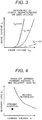
- Fig. 4 is a diagram showing the relations between forward voltages (Vf) and recovery losses (Err).
- a dotted line shows the relation between the forward voltage and the recovery loss of a conventional pin diode.
- the forward voltage (Vf) and the recovery loss (Err) are respectively minimized by dynamically controlling the gate voltage in one period of switching, therefore the trade-off characteristic is improved.
- Patent Literature 1 and Patent Literature 2 the trade-off between the forward voltage (Vf) and the recovery loss is improved, and a large amount of loss reduction can be realized.
- the inventors of this application and others found that, when they examined the recovery characteristic of each of the examples of public knowledges under the condition that an anode current was small, there was a problem in that the voltage and the current vibrated. The vibrations of the voltage and the current became more remarkable at a room temperature than at a high temperature.
- a depletion layer at the cathode side has a tendency to increase in length.
- the depletion layer which increases in length during the period of a tail current, discharges charges remaining at the cathode side, which brings about the vibrations of the voltage and the current.
- the details of a mechanism in which, if the depletion layer at the cathode side has a tendency to increase in length, the vibrations of the voltage and the current occur, are described in detail in the abovementioned Nonpatent Literature 1.
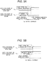
- Fig. 5a shows a first gate drive sequence of this embodiment in the case of the anode current being equal to the rated current
- Fig. 5b shows a first gate drive sequence of this embodiment in the case of the anode current being small.
- it is difficult to quantitatively define a small current, it is typically a tenth of the rated current or smaller to a half of the rated current or smaller.
- the voltage applied to the gate of the MOS-controlled diode is switched from a positive voltage (a high charge-injection mode) to a negative voltage (a low charge-injection mode) just before an IGBT of the counterpart arm of the MOS-controlled diode is turned on (that is, just before the recovery of the diode), so that the recovery loss is reduced.
- the voltage applied to the gate of the MOS-controlled diode is held positive (held in the high charge-injection mode), so that the hole density at the cathode side is held high.
- the merit (the vibration suppression) according to the present invention gains an advantage over the demerit (increase of the loss).
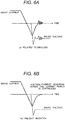
- Fig. 6a and Fig. 6b are diagrams showing the waveforms of anode currents and anode voltages respectively in the case of small current recoveries.
- Fig. 6a shows a related drive method of the gate of a MOS-controlled diode in which a voltage applied to the gate is switched from a positive voltage (the high charge-injection mode) to a negative voltage (the low charge-injection mode)
- Fig. 6b shows a drive method of the gate of a MOS-controlled diode according to the present invention in which a voltage applied to the gate is held positive (in the high charge-injection mode).
- an anode current is abruptly reduced during the period of a tail current, and vibrations occur in the anode current and the anode voltage. On the other hand, such vibrations do not occur in the drive method according to the present invention.
- Fig. 7 shows a second gate drive sequence according to the present invention.
- the voltage of the gate of the MOS-controlled diode is held positive (in the high charge-injection mode) during the period of recovery, while, in Fig. 7 , the voltage of the gate is switched to a negative voltage (to the low charge-injection mode) at the timing when the anode voltage decreases (that is, when the cathode voltage increases).
- the losses and the vibrations can be reduced, therefore the streamlining, downsizing, and cost reduction of a semiconductor apparatus and a power conversion apparatus using the same can be realized.
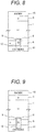
- Fig. 8 is the cross-section view of a semiconductor element according to the second embodiment of the present invention.
- This embodiment is different from the first embodiment in that this embodiment has no p + type cathode layer 13.
- an n type storage layer is formed at the interface between a gate electrode 8 and an n type cathode layer 6 by applying a higher voltage to the gate electrode 8 than to a cathode electrode 11, and it is suppressed that holes injected from a p type anode layer 3 is discharged into a cathode electrode 11, with the result that a forward voltage (Vf) is lowered (it means that a conductivity loss is reduced).
- Vf forward voltage
- a p type inversion layer is formed at the interface between the gate electrode 8 and the n type cathode layer 6 by applying a lower voltage to the gate electrode 8 than to the cathode electrode 11, and holes injected from the p type anode layer 3 is acceleratedly discharged into the cathode electrode 11, with the result that a recovery loss is reduced.
- the vibrations of an anode voltage and an anode current can be suppressed by controlling the gate voltage of a MOS-controlled diode in accordance with the anode current in a similar way as shown in Fig. 5a and Fig. 5b in the case of small current recoveries.
- the losses and the vibrations can be reduced, therefore the streamlining, downsizing, and cost reduction of a semiconductor apparatus and a power conversion apparatus using the same can be realized.
- a third embodiment of the present invention (the cross-section structure of a semiconductor element having no p type layer at a cathode side and a gate electrode stretching to a cathode electrode side) will be explained.
- Fig. 9 is the cross-section view of the semiconductor element according to the third embodiment of the present invention.
- This embodiment has a different point from the second embodiment in that a gate electrode 8 at a cathode electrode 11 side lies over the front surface of an n type cathode layer 6 (from a view point of to which direction the gate electrode lies, to the upper direction or to the lower direction of Fig. 9 , it lies to the lower direction).
- the gate electrode 8 covers the n type cathode layer 6 in the depth direction, therefore it becomes easier to control the potential of the n type cathode layer 6 using the gate electrode 8, which makes it possible to reduce losses and suppress vibrations.
- the vibrations of an anode voltage and an anode current can be suppressed by controlling the gate voltage of a MOS-controlled diode in accordance with the anode current in a similar way as shown in Fig. 5a and Fig. 5b in the case of small current recoveries.
- the losses and the vibrations can be reduced, therefore the streamlining, downsizing, and cost reduction of a semiconductor apparatus and a power conversion apparatus using the same can be realized.
- Fig. 10 is the cross-section view of the semiconductor element according to the fourth embodiment of the present invention.
- This embodiment has a different point from the first embodiment in that a gate electrode 8 is not a trench type electrode but a planar type electrode. As is the case with the first embodiment, it is possible that losses are reduced and vibrations are suppressed in this embodiment as well.
- the vibrations of an anode voltage and an anode current can be suppressed by controlling the gate voltage of a MOS-controlled diode in accordance with the anode current in a similar way as shown in Fig. 5a and Fig. 5b in the case of small current recoveries.
- the losses and the vibrations can be reduced, therefore the streamlining, downsizing, and cost reduction of a semiconductor apparatus and a power conversion apparatus using the same can be realized.
- Fig. 11 is the cross-section view of the semiconductor element according to the fifth embodiment of the present invention.
- This embodiment is different from the fifth embodiment in that this embodiment has no p + type cathode layer 13.
- this embodiment it is possible that losses are reduced and vibrations are suppressed in this embodiment as well.
- the vibrations of an anode voltage and an anode current can be suppressed by controlling the gate voltage of a MOS-controlled diode in accordance with the anode current in a similar way as shown in Fig. 5a and Fig. 5b in the case of small current recoveries.
- the losses and the vibrations can be reduced, therefore the streamlining, downsizing, and cost reduction of a semiconductor apparatus and a power conversion apparatus using the same can be realized.
- Patent Literature 3 As related technical literatures disclosing a structure in which a MOS gate is fabricated at the collector side of an IGBT, the abovementioned Patent Literature 3, Patent Literature 4, and Patent Literature 5 can be cited.
- Patent Literature 4 As related technical literatures disclosing a structure in which a MOS gate is fabricated at the collector side of an IGBT, the abovementioned Patent Literature 3, Patent Literature 4, and Patent Literature 5 can be cited.
- attention is focused on the reduction of a switching loss, but there is no description about the reduction of a vibration.
- the MOS gate is controlled while attention is focused only on the reduction of a turnoff loss.
- Fig. 12 is the cross-section view of a semiconductor element according to the sixth embodiment of the present invention.
- the structure of the collector side (rear surface) is the same as that of the cathode side (rear surface) of the first embodiment, this embodiment is different from the first embodiment in that a gate electrode 43 is fabricated at the emitter side of this embodiment.
- This embodiment includes: an n - type drift layer 1; an n type collector layer 6; a gate electrode 8; a gate insulating film 9; an insulating film 12; p + type cathode layer 13; an emitter electrode 40; a collector electrode 41; a p type channel layer 42; a gate electrode 43; and n + type emitter layer 44.
- the gate electrode 43 controls the on/off action of the collector current
- the gate electrode 8 controls the charge distribution of the n - type drift layer 1.
- an n type storage layer is formed at the interface between the gate electrode 8 and the n type cathode layer 6 by applying a positive voltage to the gate electrode 8 with respect the collector electrode 41 just before the turnoff of the IGBT (that is, just before switching the voltage of the gate electrode 43 from a positive voltage to a zero volt or to a negative voltage), and the injection of holes from a p + type cathode layer 13 is suppressed, with the result that a turnoff loss is reduced.
- Fig. 13 is a diagram showing the hole density distribution between the emitter and the collector during the time of conduction.
- p type inversion layer it is not indispensable that the absolute value of the negative gate voltage is larger than the "threshold (absolute value)" of the n type cathode layer 6, and even if the absolute value of the negative gate voltage is smaller than the "threshold (absolute value)", because the potential of the relevant channel relative to holes is lowered, the holes are injected into the n- type drift layer 1 from the p+ type cathode layer 13 via the channel route whose potential is lowered.
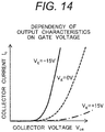
- Fig. 14 is a diagram showing the output characteristics when the positive voltage, 0 V voltage, and the negative voltage are applied to the gate electrode 8 respectively.
- the negative voltage is applied to the gate electrode 8 because the hole density at the collector side is high (as shown in Fig. 13 ), the collector current is large (it means that the on-voltage is small).
- the collector current becomes small (it means that the on-voltage becomes large).
- the positive voltage is applied to the gate electrode 8, because the hole density at the collector side is much more lowered, the collector current becomes smaller (it means that the on-voltage becomes larger).
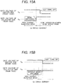
- Fig. 15a and Fig. 15b are diagrams showing the gate drive sequences of this embodiment.
- Fig. 15a is a diagram showing the gate drive sequence in the case where the collector current is equal to its rated current
- Fig. 15b is a diagram showing the gate drive sequence in the case where the collector current is a small current.
- it is difficult to quantitatively define a small current, it is typically a tenth of the rated current or smaller to a half of the rated current or smaller.
- the voltage applied to the gate at the collector side (rear surface) is switched to a positive voltage just before the gate voltage at the emitter side (front surface) is turned off (that is, just before the collector current of the IGBT is turned off) to switch from the high charge-injection mode to the low charge-injection (high speed) mode), so that the turnoff loss is reduced.
- the voltage applied to the gate at the collector side (rear surface) is held negative (held in the high charge-injection mode), so that the hole density at the collector side is held high to suppress the vibrations.
- the losses and the vibrations can be reduced, therefore the streamlining, downsizing, and cost reduction of a semiconductor apparatus and a power conversion apparatus using the same can be realized.
- Fig. 16 is the cross-section view of the semiconductor element according to the seventh embodiment of the present invention.
- This embodiment has a different point from the sixth embodiment in that a gate electrode 8 is not a trench type electrode but a planar type electrode.
- a gate electrode 8 is not a trench type electrode but a planar type electrode.
- the vibrations of a collector voltage and a collector current can be suppressed by controlling the gate voltage at the collector side (rear surface) in accordance with the collector current in a similar way as shown in Fig. 15a and Fig. 15b at the time of the small current turnoff of the IGBT.
- This embodiment is an embodiment of a circuit for driving a semiconductor element (MOS-controlled diode) used in any of the above-described first to fifth embodiments.
- Fig. 17 is the circuit diagram of a drive circuit according to this embodiment.
- This embodiment includes: a control circuit 20; IGBT drive circuits 21; drive circuits 22 for driving semiconductor apparatuses according to the first to fifth embodiments; an upper arm IGBT 23; a lower arm IGBT 24; a semiconductor apparatus 25 that is described in any of the above-described first to fifth embodiments and applied to the upper arm; a semiconductor apparatus 26 that is described in any of the above-described first to fifth embodiments and applied to the lower arm; and a current detector 30.
- Circuit signs used for the semiconductor apparatuses 25 and 26 respectively represent the resistor values of diodes each of which is controlled by the relevant gate electrode, and these circuit signs are devised by the inventors and others for the purpose of convenience, and they are not common signs.
- the current detector 30 is a detector for detecting a current flowing through a diode, it is also possible to indirectly detect the current flowing through the diode by detecting the relevant IGBT current. Furthermore, it is also possible to estimate the diode current by detecting the motor current. Which of the gate drive sequence in the case of the rated current and the gate drive sequence in the case of a small current should be selected is determined in accordance with the collector current detected by the current detector 30 by the control circuit 20.
- the losses and the vibrations can be reduced by detecting a diode current, and therefore the streamlining, downsizing, and cost reduction of a semiconductor apparatus and a power conversion apparatus using the same can be realized.
- the feature of this embodiment is the fact that diodes explained in the first to the fifth embodiments are applied to flywheel diodes 600.
- diodes explained in the first to the fifth embodiments are applied to flywheel diodes 600.
- the feature of this embodiment is the fact that IGBTs explained in the sixth and the seventh embodiments are applied to the IGBTs 700.
- the losses in the diodes are reduced, which makes it possible to realize the reduction of the losses and downsizing of the inverter.
- the configuration of the inverter apparatus shown in Fig. 18 is an example, and an apparatus, which has the same number of serial-connected combinations, each of which includes a switching element and a diode reversely connected, as the number of the phases of an alternating current output, also has the same advantageous effect.
Landscapes
- Engineering & Computer Science (AREA)
- Power Engineering (AREA)
- Power Conversion In General (AREA)
- Inverter Devices (AREA)
- Electronic Switches (AREA)
- Thyristors (AREA)
Applications Claiming Priority (1)
| Application Number | Priority Date | Filing Date | Title |
|---|---|---|---|
| PCT/JP2014/052196 WO2015114787A1 (ja) | 2014-01-31 | 2014-01-31 | 半導体素子の駆動装置およびそれを用いた電力変換装置 |
Publications (2)
| Publication Number | Publication Date |
|---|---|
| EP3101809A1 true EP3101809A1 (de) | 2016-12-07 |
| EP3101809A4 EP3101809A4 (de) | 2017-08-23 |
Family
ID=53756399
Family Applications (1)
| Application Number | Title | Priority Date | Filing Date |
|---|---|---|---|
| EP14881018.7A Withdrawn EP3101809A4 (de) | 2014-01-31 | 2014-01-31 | Halbleiterelementansteuerungsvorrichtung leistungswandlervorrichtung damit |
Country Status (5)
| Country | Link |
|---|---|
| US (1) | US20160343838A1 (de) |
| EP (1) | EP3101809A4 (de) |
| JP (1) | JP6227677B2 (de) |
| CN (1) | CN105940606B (de) |
| WO (1) | WO2015114787A1 (de) |
Families Citing this family (12)
| Publication number | Priority date | Publication date | Assignee | Title |
|---|---|---|---|---|
| JP6742925B2 (ja) * | 2017-01-18 | 2020-08-19 | 株式会社 日立パワーデバイス | 半導体装置、及びそれを用いた電力変換装置 |
| WO2019038755A1 (en) | 2017-08-24 | 2019-02-28 | Segasec Labs Ltd | DOMAIN USURPATION IDENTIFICATION SYSTEM |
| JP6820287B2 (ja) * | 2018-02-23 | 2021-01-27 | 株式会社 日立パワーデバイス | 半導体装置および電力変換装置 |
| JP6964538B2 (ja) * | 2018-02-28 | 2021-11-10 | 株式会社 日立パワーデバイス | 半導体装置および電力変換装置 |
| JP7068981B2 (ja) * | 2018-09-25 | 2022-05-17 | 三菱電機株式会社 | 半導体装置 |
| JP7246983B2 (ja) | 2019-03-20 | 2023-03-28 | 株式会社東芝 | 半導体装置 |
| CN113728443B (zh) * | 2019-04-02 | 2024-04-05 | 日立能源有限公司 | 改进反向恢复的分段功率二极管结构 |
| JP7315443B2 (ja) * | 2019-12-06 | 2023-07-26 | 株式会社日立製作所 | 半導体回路制御方法、及びそれを適用した電力変換器 |
| JP7444027B2 (ja) * | 2020-11-06 | 2024-03-06 | 三菱電機株式会社 | 半導体装置 |
| JP7722648B2 (ja) * | 2020-12-04 | 2025-08-13 | 国立大学法人 東京大学 | 半導体装置 |
| CN114203810A (zh) * | 2021-12-10 | 2022-03-18 | 电子科技大学 | 一种增加背面栅降低关断损耗的超高压igbt结构 |
| JP7814817B2 (ja) * | 2022-09-27 | 2026-02-17 | 三菱電機株式会社 | 半導体装置の制御方法 |
Family Cites Families (14)
| Publication number | Priority date | Publication date | Assignee | Title |
|---|---|---|---|---|
| JP3075007B2 (ja) * | 1992-05-01 | 2000-08-07 | 富士電機株式会社 | スイッチング装置及びダブルゲート型半導体装置の制御装置 |
| JP3779401B2 (ja) | 1996-11-29 | 2006-05-31 | 株式会社東芝 | ダイオードの駆動方法 |
| JP4479052B2 (ja) | 2000-05-09 | 2010-06-09 | 富士電機システムズ株式会社 | 半導体装置 |
| JP5277579B2 (ja) * | 2007-07-25 | 2013-08-28 | 日産自動車株式会社 | 半導体装置 |
| JP5417811B2 (ja) | 2008-11-18 | 2014-02-19 | 株式会社デンソー | 半導体装置 |
| JP5446233B2 (ja) * | 2008-12-08 | 2014-03-19 | 株式会社デンソー | 絶縁ゲート型半導体装置の駆動回路およびそれに適した半導体装置 |
| JP2010251517A (ja) * | 2009-04-15 | 2010-11-04 | Tokyo Electric Power Co Inc:The | パワー半導体素子 |
| JP2010283132A (ja) * | 2009-06-04 | 2010-12-16 | Mitsubishi Electric Corp | 半導体装置 |
| JP5171776B2 (ja) * | 2009-09-30 | 2013-03-27 | 株式会社日立製作所 | 半導体装置、及びそれを用いた電力変換装置 |
| JP5229288B2 (ja) * | 2010-09-20 | 2013-07-03 | 株式会社デンソー | 半導体装置およびその制御方法 |
| DE102011079747A1 (de) * | 2010-07-27 | 2012-02-02 | Denso Corporation | Halbleitervorrichtung mit Schaltelement und Freilaufdiode, sowie Steuerverfahren hierfür |
| US9349847B2 (en) * | 2011-12-15 | 2016-05-24 | Hitachi, Ltd. | Semiconductor device and power converter |
| JP6015745B2 (ja) * | 2012-03-19 | 2016-10-26 | 富士電機株式会社 | 半導体装置の製造方法 |
| DE112013006639T5 (de) * | 2013-02-25 | 2015-10-29 | Hitachi, Ltd. | Halbleitervorrichtung, Treibervorrichtung für eine Halbleiterschaltung und Leistungswandlungsvorrichtung |
-
2014
- 2014-01-31 EP EP14881018.7A patent/EP3101809A4/de not_active Withdrawn
- 2014-01-31 WO PCT/JP2014/052196 patent/WO2015114787A1/ja not_active Ceased
- 2014-01-31 JP JP2015559682A patent/JP6227677B2/ja not_active Expired - Fee Related
- 2014-01-31 US US15/114,513 patent/US20160343838A1/en not_active Abandoned
- 2014-01-31 CN CN201480074434.4A patent/CN105940606B/zh not_active Expired - Fee Related
Also Published As
| Publication number | Publication date |
|---|---|
| US20160343838A1 (en) | 2016-11-24 |
| EP3101809A4 (de) | 2017-08-23 |
| JP6227677B2 (ja) | 2017-11-08 |
| CN105940606A (zh) | 2016-09-14 |
| JPWO2015114787A1 (ja) | 2017-03-23 |
| CN105940606B (zh) | 2018-10-12 |
| WO2015114787A1 (ja) | 2015-08-06 |
Similar Documents
| Publication | Publication Date | Title |
|---|---|---|
| EP3101809A1 (de) | Halbleiterelementansteuerungsvorrichtung leistungswandlervorrichtung damit | |
| US9627878B2 (en) | Driving device for semiconductor elements, and semiconductor device | |
| US7638839B2 (en) | Power semiconductor device and power conversion device using the same | |
| US20150003133A1 (en) | Drive Circuit of Semiconductor Switching Element and Power Conversion Circuit Using the Same | |
| CN111788695B (zh) | 半导体装置以及电力变换装置 | |
| CN109962699A (zh) | 用于控制mosfet开关模块的方法和装置 | |
| US11043943B2 (en) | Switching of paralleled reverse conducting IGBT and wide bandgap switch | |
| CN105191132A (zh) | 绝缘栅型半导体元件的控制装置以及使用了该控制装置的电力变换装置 | |
| Kadavelugu et al. | Understanding dv/dt of 15 kV SiC N-IGBT and its control using active gate driver | |
| WO2017221417A1 (ja) | ゲート駆動回路、電力変換装置および鉄道車両 | |
| JP2014147237A (ja) | 半導体装置のゲート駆動回路およびそれを用いた電力変換装置 | |
| Baburske et al. | Comparison of critical current filaments in IGBT short circuit and during diode turn-off | |
| US20160013299A1 (en) | Semiconductor device, drive device for semiconductor circuit, and power conversion device | |
| Papadopoulos et al. | BIGT control optimisation for overall loss reduction | |
| CN112786697A (zh) | 半导体装置的控制方法 | |
| US20160013300A1 (en) | Semiconductor device, drive device for semiconductor circuit, and power conversion device | |
| EP4071813B1 (de) | Verfahren zur steuerung eines halbleiterschaltkreises und elektrischer leistungswandler, bei dem es angewendet wird | |
| Eckel et al. | Turn-off behaviour of high voltage NPT-and FS-IGBT | |
| JP6338145B2 (ja) | 半導体装置及びそれを用いた電力変換装置 | |
| Baburske et al. | Passive turn-on process of IGBTs in Matrix converter applications | |
| Nayampalli et al. | Desaturated turn-off of low-saturation IGBTs with clamping method to reduce turn-off energy losses | |
| WO2014086015A1 (zh) | 一种ti-igbt及其形成方法 | |
| EP1793423A2 (de) | Halbleiterspannungsvorrichtung und diese Halbleiterspannungsvorrichtung verwendende Spannungsumwandlungsvorrichtung | |
| Chen et al. | The SuperJunction MOS-controlled thyristor (SJ-MCT) with low power loss for high-power switching applications | |
| JP6840053B2 (ja) | 半導体電力変換回路、並びにそれを用いた半導体装置及びモータ駆動装置 |
Legal Events
| Date | Code | Title | Description |
|---|---|---|---|
| PUAI | Public reference made under article 153(3) epc to a published international application that has entered the european phase |
Free format text: ORIGINAL CODE: 0009012 |
|
| STAA | Information on the status of an ep patent application or granted ep patent |
Free format text: STATUS: REQUEST FOR EXAMINATION WAS MADE |
|
| 17P | Request for examination filed |
Effective date: 20160831 |
|
| AK | Designated contracting states |
Kind code of ref document: A1 Designated state(s): AL AT BE BG CH CY CZ DE DK EE ES FI FR GB GR HR HU IE IS IT LI LT LU LV MC MK MT NL NO PL PT RO RS SE SI SK SM TR |
|
| AX | Request for extension of the european patent |
Extension state: BA ME |
|
| DAX | Request for extension of the european patent (deleted) | ||
| A4 | Supplementary search report drawn up and despatched |
Effective date: 20170725 |
|
| RIC1 | Information provided on ipc code assigned before grant |
Ipc: H01L 29/739 20060101ALI20170719BHEP Ipc: H03K 17/16 20060101AFI20170719BHEP Ipc: H03K 17/74 20060101ALI20170719BHEP Ipc: H03K 17/687 20060101ALI20170719BHEP Ipc: H01L 29/78 20060101ALI20170719BHEP |
|
| STAA | Information on the status of an ep patent application or granted ep patent |
Free format text: STATUS: EXAMINATION IS IN PROGRESS |
|
| STAA | Information on the status of an ep patent application or granted ep patent |
Free format text: STATUS: THE APPLICATION HAS BEEN WITHDRAWN |
|
| 17Q | First examination report despatched |
Effective date: 20190103 |
|
| 18W | Application withdrawn |
Effective date: 20181220 |