EP3104407B1 - Mobiles endgerät - Google Patents
Mobiles endgerät Download PDFInfo
- Publication number
- EP3104407B1 EP3104407B1 EP14886216.2A EP14886216A EP3104407B1 EP 3104407 B1 EP3104407 B1 EP 3104407B1 EP 14886216 A EP14886216 A EP 14886216A EP 3104407 B1 EP3104407 B1 EP 3104407B1
- Authority
- EP
- European Patent Office
- Prior art keywords
- circuit board
- chip
- heat pipe
- heat
- mobile terminal
- Prior art date
- Legal status (The legal status is an assumption and is not a legal conclusion. Google has not performed a legal analysis and makes no representation as to the accuracy of the status listed.)
- Active
Links
Images

Classifications
-
- H—ELECTRICITY
- H10—SEMICONDUCTOR DEVICES; ELECTRIC SOLID-STATE DEVICES NOT OTHERWISE PROVIDED FOR
- H10W—GENERIC PACKAGES, INTERCONNECTIONS, CONNECTORS OR OTHER CONSTRUCTIONAL DETAILS OF DEVICES COVERED BY CLASS H10
- H10W40/00—Arrangements for thermal protection or thermal control
- H10W40/70—Fillings or auxiliary members in containers or in encapsulations for thermal protection or control
- H10W40/73—Fillings or auxiliary members in containers or in encapsulations for thermal protection or control for cooling by change of state
-
- H—ELECTRICITY
- H10—SEMICONDUCTOR DEVICES; ELECTRIC SOLID-STATE DEVICES NOT OTHERWISE PROVIDED FOR
- H10W—GENERIC PACKAGES, INTERCONNECTIONS, CONNECTORS OR OTHER CONSTRUCTIONAL DETAILS OF DEVICES COVERED BY CLASS H10
- H10W40/00—Arrangements for thermal protection or thermal control
- H10W40/01—Manufacture or treatment
- H10W40/03—Manufacture or treatment of arrangements for cooling
- H10W40/037—Assembling together parts thereof
-
- H—ELECTRICITY
- H10—SEMICONDUCTOR DEVICES; ELECTRIC SOLID-STATE DEVICES NOT OTHERWISE PROVIDED FOR
- H10W—GENERIC PACKAGES, INTERCONNECTIONS, CONNECTORS OR OTHER CONSTRUCTIONAL DETAILS OF DEVICES COVERED BY CLASS H10
- H10W40/00—Arrangements for thermal protection or thermal control
- H10W40/20—Arrangements for cooling
- H10W40/22—Arrangements for cooling characterised by their shape, e.g. having conical or cylindrical projections
Definitions
- the present invention relates to the field of terminal technologies, and in particular, to a mobile terminal.
- a heat-conducting layer is generally disposed between a chip and a shielding case of the chip. Heat generated by the chip is conducted to the shielding case by the heat-conducting layer, and is then dissipated by means of a heat conduction effect of the shielding case that is made of a metal, thereby achieving heat dissipation of the chip and lowering a temperature around the chip.
- EP 0 917 418 A1 discloses an electronic apparatus being contained in a heat dissipative external enclosure 2.
- the enclosure contains at least one unit contained in a thermally conductive internal housing 4,6 providing RF isolation and mounted on a wall 7 of the enclosure in thermal contact therewith.
- a wall 11 of the unit has a first recess 14 receiving the evaporator 13 of a heat pipe 12.
- the heat pipe is clamped between the external enclosure and the internal housing.
- the condenser 22 of the heat pipe is lower than the evaporator and is received by a recess 24 in the wall 7.
- the evaporator is clamped in the recess by a clamp member e.g. another unit 6.
- JP H11 68371 A discloses a laminated multilayered wiring board.
- a through hole 20 is formed at a position which is facing to a heat-generating part 11 of an electronic circuit on the board.
- a heat pipe 16 is inserted into through hole 20 so that one end of the heat pipe 16 is thermally coupled to the heat- generating part 11, while the other end of the pipe 16 is thermally coupled to a heat radiator 15.
- the heat generated by the part 11 is transferred to the heat radiator 15 through the heat pipe 16 to thermally control the part 11.
- US 6 122 167 A discloses a computer system including a motherboard mounted in a chassis.
- An EMI shield member is mounted on the motherboard.
- a processor module is connected to the motherboard and has peripheral edge contact with the EMI shield member.
- a cap member is mounted on the processor module and is engaged with the EMI shield member.
- a heat sink is connected to the cap member.
- a heat pipe has a first end attached to the cap member and a second end attached to the heat sink.
- a fan is mounted in the chassis adjacent the heat sink for drawing cooling air across the heat sink.
- JP H06 244576 A discloses a printed wiring board 1 with an unified heat pipe consisting of the following; a first single-sided copper-clad lamination board 15 on which a mounting parts like an IC 20 as a heat generating element is arranged, a second single-sided copper-clad lamination board 16, and a heat pipe 5 which dissipates the heat generated from the IC 20 mounted on the single-sided copper- clad lamination boards 15, 16.
- the heat pipe 5 consists of an evaporation part 3 for vaporizing operating liquid sealed in the heat pipe 5 and a condenser part 4 for liquifying the vaporized operating liquid.
- the evaporation part 3 is arranged in the vicinity of the heat generating element on the single-sided copper-clad lamination board 15.
- the condenser part 4 are made to protrude outside the single-sided copper clad lamination boards 15, 16, and dissipates the heat.
- EP 0 529 837 A1 discloses a method and apparatus for cooling a multi-chip module with an integrated heatpipe (38).
- Multiple semiconductor chips (10) are embedded in a packaging substrate (12) with electrical interconnects disposed on one side while a heat sink (14) incorporated into the substrate on the other side and abutting the semiconductor chips on their underside.
- a heatpipe (38) is directly mounted to the heat sink. Inside the heatpipe is a chamber containing a coolant (18) and a wick (16).
- JP H03 25991 A discloses printed circuit board with a heat absorption layer 2 made of a copper foil having substantially the same size as that of an insulating plate 1 made of a glass epoxy resin laminated plate is secured to one side face of the plate 1.
- Three heat pipes 3 made of copper pipes sealed in operation liquid therein are secured substantially at an equal interval to the layer 2.
- the part not in contact with the layer 2 is secured to one side face of a base material 4 made of epoxy resin.;
- Heats generated from an element and a conductor pattern mounted on the plate 1 are transferred to the pipes 3 through the layer 2 to evaporate the liquids in the pipes 3, the heat of the vapor is dissipated by the evaporation at a heat sink 31.
- a technical problem to be resolved by the present invention is to provide a mobile terminal which can improve a heat dissipation effect of a chip and lower a temperature of the chip.
- a mobile terminal includes a circuit board, where a chip is disposed on a first surface of the circuit board, a groove is provided on a second surface of the circuit board, and the mobile terminal further includes: a heat pipe, where one end of the heat pipe is embedded in the groove, and an other end of the heat pipe protrudes from a side wall of the circuit board or is flush to a side wall of the circuit board.
- the groove extends to below the chip, so that one end of the heat pipe extends to below the chip.
- the depth of the groove is less than or equal to half a thickness of the circuit board.
- the mobile terminal further includes: a thermal pad, located in the groove, where the thermal pad is located between the chip and the heat pipe.
- the heat pipe has a rectangular section.
- the mobile terminal further includes: a shielding case, located on the circuit board and wrapping the chip.
- the mobile terminal further includes: a housing, wrapping the heat pipe, the shielding case, the chip, and the circuit board.
- the chip is disposed on the first surface of the circuit board in the mobile terminal, the groove is provided on the second surface of the circuit board, the heat pipe is disposed in the groove, and one end of the heat pipe extends to the side wall of the circuit board or outside the side wall of the circuit board, so that heat generated by the chip can be conducted to outside the circuit board through the heat pipe.
- a temperature around the chip can be effectively lowered, thereby lowering a temperature of the entire mobile terminal.
- a leakage current is reduced, and power consumption of the chip is reduced, thereby further reducing power consumption of the entire mobile terminal.
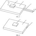
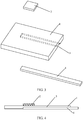
- an embodiment of the present invention provides a mobile terminal, including a circuit board 1, where a chip 2 is disposed on a first surface of the circuit board 1, and a groove 3 is provided on a second surface of the circuit board 1.
- the mobile terminal further includes:
- the heat pipe 4 makes use of evaporative cooling, so that temperatures of two ends of the heat pipe differ greatly and heat is conducted rapidly.
- the heat pipe generally consists of an envelope, a wick and end caps. An interior of the heat pipe is exhausted to a negative-pressure state and filled with a suitable liquid. Such a liquid has a low boiling point and is volatile.
- a pipe wall is provided with a wick that is made of a capillary porous material.
- the one end of the heat pipe 4 is an evaporation end, and the other end is a condensation end. When the one end of the heat pipe is heated, the liquid in capillary tubes evaporates rapidly. Vapor flows to the other end under a tiny pressure difference, releases heat and condenses into a liquid again.
- the chip 2 is disposed on the first surface of the circuit board 1
- the groove 3 is provided on the second surface of the circuit board 1
- the groove 3 extends to below the chip 2
- the heat pipe 4 is disposed in the groove 3
- one end of the heat pipe 4 extends to outside the side wall of the circuit board 1.
- the heat pipe 4 can conduct heat generated by the chip 2 to an area with a relatively low temperature outside the circuit board 1, which effectively lowers a temperature around the chip 2, improves the heat dissipation efficiency of the chip 2, and lowers a temperature of the chip 2.
- the chip 2 is integrated with multiple electronic devices that enable the chip 2 to implement its functions, such as a MOS (Metal Oxide Semiconductor) transistor, when the temperature of the chip 2 rises, a leakage current from a source to a drain of the MOS transistor increases exponentially with the temperature, and power consumption of the chip 2 is increased.
- MOS Metal Oxide Semiconductor
- the heat dissipation efficiency of the chip 2 is improved, the temperature around the chip 2 is lowered, and the leakage current is reduced, which is equivalent to reducing the power consumption of the chip 2, thereby further reducing power consumption of the entire mobile terminal.
- the heat pipe 4 may extend only to the side wall of the circuit board 1. In this way, not only the temperature around the chip 2 can be lowered, but also a length of the mobile terminal can be shortened.
- the chip is disposed on the first surface of the circuit board in the mobile terminal, the groove is provided on the second surface of the circuit board, the heat pipe is disposed in the groove, and one end of the heat pipe extends to the side wall of the circuit board or outside the side wall of the circuit board, so that heat generated by the chip can be conducted to the outside of the circuit board through the heat pipe.
- a temperature around the chip can be effectively lowered, thereby lowering a temperature of the entire mobile terminal.
- a leakage current is reduced, and power consumption of the chip is reduced, thereby further reducing power consumption of the entire mobile terminal.
- the depth of the groove 3 is set according to an actual thickness of the circuit board 1. Because the thickness of the circuit board 1 ranges from 0.6 mm to 1 mm, the depth of the groove 3 should be less than or equal to half the thickness of the circuit board 1, in order to ensure strength and rigidity of the circuit board 1 provided with the groove 3.
- a heat pipe 4 having a rectangular section, preferably a relatively oblate rectangular section, may be selected. In this case, the depth of the groove 3 cooperating with the heat pipe 4 can be relatively small, which can better ensure the strength and rigidity of the circuit board 1.
- a heat pipe having a relatively large width may be selected, which can ensure a heat dissipation effect of the chip 2.
- a circuit board 1 of a mobile terminal has a thickness of 0.65 mm and is of a 10-layer board structure.
- a heat pipe 4 having a thickness of 0.5 mm and a length of 100 mm may be selected. Because a depth of a groove 3 in the circuit board 1 should not exceed half the thickness of the circuit board 1, the groove 3 may be formed on a second surface of the circuit board 1.
- the groove 3 has a depth of 0.2 mm and extends from a side wall of the circuit board 1 to a position, which corresponds to a chip 2, on the second surface. In this case, the heat pipe 4 protrudes from the second surface of the circuit board 1 by 0.3 mm.
- the groove 3 may be formed by using a milling cutter machine, or be formed by using a laser method.
- the laser method is only applicable to a circuit board 1 that is not clad with copper, and a material that is not transmissive to a laser needs to be disposed between layers.
- a material that is not transmissive to a laser may be disposed between the third and fourth layers of the structure.
- the mobile terminal in the present invention may further include: a thermal pad 5, located in the groove 3, where the thermal pad 5 is located between the chip 2 and the heat pipe 4.
- the thermal pad 5 is made of a high-performance, thermally conductive gap-filling material, which is mainly used for a transfer interface between an electronic device and a heat sink or a housing of the electronic device, and has good stickiness, good flexibility, good compression performance and an excellent thermal conductivity.
- the thermal pad 5 is placed between the heat pipe 4 and the chip 2, to conduct heat from the chip 2 to the heat pipe 4, thereby further improving the heat dissipation efficiency of the chip 2 and lowering the temperature of the chip 2.
- the mobile terminal further includes: a shielding case, located on the circuit board 1 and wrapping the chip 2; and a structure such as a housing that wraps the heat pipe 4, the shielding case, the chip 2, and the circuit board 1.
Landscapes
- Cooling Or The Like Of Electrical Apparatus (AREA)
- Cooling Or The Like Of Semiconductors Or Solid State Devices (AREA)
- Telephone Set Structure (AREA)
- Shielding Devices Or Components To Electric Or Magnetic Fields (AREA)
Claims (4)
- Mobilendgerät, das eine Schaltungsplatine (1) umfasst, wobei ein Chip (2) auf einer ersten Oberfläche der Schaltungsplatine (1) angeordnet ist, die Schaltungsplatine eine Dicke in einem Bereich von 0,6 mm bis 1 mm aufweist,
eine Nut (3) auf einer zweiten Oberfläche der Schaltungsplatine (1) vorgesehen ist, wobei sich die Nut (3) bis unter den Chip erstreckt und sich bis zu einer Seitenwand der Schaltungsplatine (1) erstreckt und eine Tiefe der Nut (3) kleiner oder gleich einer halben Dicke der Schaltungsplatine (1) ist, und das Mobilendgerät ferner Folgendes umfasst:eine "Heat-Pipe" (4), wobei die "Heat-Pipe" (4) in der Nut (3) angeordnet ist und sich ein Ende der "Heat-Pipe" (4) bis zur Seitenwand der Schaltungsplatine (1) oder nach außerhalb der Seitenwand der Schaltungsplatine (1) erstreckt, undein Wärmeübertragungselement (5), das sich in der Nut (3) befindet, wobei sich das Wärmeübertragungselement (5) zwischen dem Chip (2) und der "Heat-Pipe" (4) befindet. - Mobilendgerät nach Anspruch 1, wobei
die "Heat-Pipe" (4) einen rechteckigen Querschnitt aufweist. - Mobilendgerät nach Anspruch 1, ferner umfassend:
eine Abschirmungseinhäusung, die sich auf der Schaltungsplatine (1) befindet und den Chip (2) umhüllt. - Mobilendgerät nach Anspruch 1, ferner umfassend:
ein Gehäuse, das die "Heat-Pipe" (4), die Abschirmungseinhäusung, den Chip (2) und die Schaltungsplatine (1) umhüllt.
Applications Claiming Priority (1)
| Application Number | Priority Date | Filing Date | Title |
|---|---|---|---|
| PCT/CN2014/073784 WO2015139271A1 (zh) | 2014-03-20 | 2014-03-20 | 一种移动终端 |
Publications (3)
| Publication Number | Publication Date |
|---|---|
| EP3104407A1 EP3104407A1 (de) | 2016-12-14 |
| EP3104407A4 EP3104407A4 (de) | 2017-03-08 |
| EP3104407B1 true EP3104407B1 (de) | 2020-09-09 |
Family
ID=54143689
Family Applications (1)
| Application Number | Title | Priority Date | Filing Date |
|---|---|---|---|
| EP14886216.2A Active EP3104407B1 (de) | 2014-03-20 | 2014-03-20 | Mobiles endgerät |
Country Status (5)
| Country | Link |
|---|---|
| US (1) | US9768096B2 (de) |
| EP (1) | EP3104407B1 (de) |
| JP (1) | JP6527879B2 (de) |
| CN (1) | CN105340075B (de) |
| WO (1) | WO2015139271A1 (de) |
Families Citing this family (11)
| Publication number | Priority date | Publication date | Assignee | Title |
|---|---|---|---|---|
| KR102546241B1 (ko) | 2016-10-05 | 2023-06-22 | 삼성전자주식회사 | 반도체 패키지 |
| CN106714515B (zh) * | 2016-12-20 | 2023-07-25 | 深圳市欢太科技有限公司 | 移动终端 |
| CN110060966B (zh) * | 2018-01-18 | 2021-09-17 | 苏州旭创科技有限公司 | 光模块 |
| CN108617081B (zh) * | 2018-06-11 | 2019-09-20 | Oppo广东移动通信有限公司 | 一种电子装置及一种电路板组件 |
| CN108777255B (zh) * | 2018-06-11 | 2020-07-31 | Oppo广东移动通信有限公司 | 一种散热组件及电子设备 |
| CN108513515B (zh) * | 2018-06-11 | 2020-10-02 | Oppo广东移动通信有限公司 | 壳体组件以及电子装置 |
| CN110798961B (zh) * | 2018-08-01 | 2022-10-21 | 苏州旭创科技有限公司 | 一种电路板及具有其的光模块 |
| CN112601347B (zh) * | 2020-12-22 | 2023-04-11 | 京东方科技集团股份有限公司 | Pcb组件与显示模组 |
| CN114615795A (zh) * | 2022-03-08 | 2022-06-10 | 惠科股份有限公司 | Pcba板组件、pcba板组件的制作方法及电子设备 |
| CN117156349A (zh) * | 2022-05-24 | 2023-12-01 | 惠州Tcl移动通信有限公司 | 电子设备 |
| CN119545660B (zh) * | 2023-08-28 | 2025-12-12 | 庆鼎精密电子(淮安)有限公司 | 电路板结构及其制造方法 |
Family Cites Families (21)
| Publication number | Priority date | Publication date | Assignee | Title |
|---|---|---|---|---|
| JP2635770B2 (ja) * | 1989-06-23 | 1997-07-30 | 古河電気工業株式会社 | プリント配線用基板 |
| EP0529837B1 (de) | 1991-08-26 | 1996-05-29 | Sun Microsystems, Inc. | Verfahren und Apparat zum Kühlen von Mehrchip-Moduln durch die vollständige Wärmerohr-Technologie |
| JPH06244576A (ja) * | 1993-02-17 | 1994-09-02 | Toshiba Corp | ヒートパイプ一体化プリント配線板 |
| WO1998041661A1 (en) | 1997-03-14 | 1998-09-24 | Nippon Steel Corporation | Steel band heat-treating apparatus by gas jet stream |
| JPH1168371A (ja) * | 1997-08-21 | 1999-03-09 | Toshiba Corp | 電子機器及びその印刷配線基板 |
| EP0917418B1 (de) | 1997-11-11 | 2003-09-17 | Lucent Technologies Inc. | Elektronisches Gerät |
| JPH11163410A (ja) * | 1997-11-25 | 1999-06-18 | Matsushita Electric Works Ltd | Led照明装置 |
| US6122167A (en) * | 1998-06-02 | 2000-09-19 | Dell Usa, L.P. | Integrated hybrid cooling with EMI shielding for a portable computer |
| JP2001177030A (ja) * | 1999-12-15 | 2001-06-29 | Sony Corp | 放熱装置及び放熱装置を有する電子機器 |
| JP2001291806A (ja) * | 2000-04-06 | 2001-10-19 | Housen Kk | ヒートシンク |
| JP2002270803A (ja) * | 2001-03-14 | 2002-09-20 | Ricoh Co Ltd | 固体撮像装置、画像読取ユニット及び画像形成装置 |
| JP2004177218A (ja) * | 2002-11-26 | 2004-06-24 | Matsushita Electric Works Ltd | 半導体加速度センサ |
| JP2004241450A (ja) * | 2003-02-04 | 2004-08-26 | Edl:Kk | ヒートシンク |
| JP2006019557A (ja) * | 2004-07-02 | 2006-01-19 | Fujikura Ltd | 発光装置とその実装方法、照明器具及びディスプレイ |
| JP2006066725A (ja) * | 2004-08-27 | 2006-03-09 | Sony Corp | 放熱構造を備える半導体装置及びその組立方法 |
| CN100444364C (zh) * | 2005-09-02 | 2008-12-17 | 富准精密工业(深圳)有限公司 | 热管散热装置 |
| KR100653605B1 (ko) * | 2005-11-15 | 2006-12-06 | 삼성전자주식회사 | 메탈 코어 히트싱크를 구비하는 반도체 칩 패키지와 그를포함하는 반도체 모듈 |
| CN101374395B (zh) * | 2007-08-24 | 2012-05-16 | 富准精密工业(深圳)有限公司 | 散热装置 |
| CN101384152B (zh) * | 2007-09-07 | 2011-07-27 | 富准精密工业(深圳)有限公司 | 散热装置 |
| JP5848874B2 (ja) * | 2011-01-07 | 2016-01-27 | 日本発條株式会社 | 温度調節装置およびこの温度調節装置の製造方法 |
| CN202362724U (zh) * | 2011-11-28 | 2012-08-01 | 双鸿科技股份有限公司 | 嵌入式散热器 |
-
2014
- 2014-03-20 CN CN201480036435.XA patent/CN105340075B/zh active Active
- 2014-03-20 WO PCT/CN2014/073784 patent/WO2015139271A1/zh not_active Ceased
- 2014-03-20 US US15/123,484 patent/US9768096B2/en active Active
- 2014-03-20 EP EP14886216.2A patent/EP3104407B1/de active Active
- 2014-03-20 JP JP2016558074A patent/JP6527879B2/ja active Active
Non-Patent Citations (1)
| Title |
|---|
| None * |
Also Published As
| Publication number | Publication date |
|---|---|
| JP6527879B2 (ja) | 2019-06-05 |
| EP3104407A4 (de) | 2017-03-08 |
| EP3104407A1 (de) | 2016-12-14 |
| US20170077010A1 (en) | 2017-03-16 |
| US9768096B2 (en) | 2017-09-19 |
| CN105340075B (zh) | 2019-09-13 |
| JP2017511646A (ja) | 2017-04-20 |
| WO2015139271A1 (zh) | 2015-09-24 |
| CN105340075A (zh) | 2016-02-17 |
Similar Documents
| Publication | Publication Date | Title |
|---|---|---|
| US9768096B2 (en) | Mobile terminal | |
| CN102460689B (zh) | 冷却装置、电子基板和电子装置 | |
| US10622282B2 (en) | Systems and methods for cooling an electronic device | |
| US6219243B1 (en) | Heat spreader structures for enhanced heat removal from both sides of chip-on-flex packaged units | |
| US11839055B2 (en) | Heat-conducting assembly and terminal | |
| CN109640588B (zh) | 终端设备 | |
| US20160095203A1 (en) | Circuit board | |
| CN107134443B (zh) | 覆晶薄膜、显示装置和集成电路的封装方法 | |
| CN105723821A (zh) | 便携式电子设备的冷却构造 | |
| TW201248109A (en) | Electronic equipment | |
| US6101094A (en) | Printed circuit board with integrated cooling mechanism | |
| CN108617082A (zh) | 一种散热组件以及电子装置 | |
| US20030021310A1 (en) | Method and apparatus for cooling electronic or opto-electronic devices | |
| US20140332185A1 (en) | Heat insulating device, method for manufacturing the same, and heat dissipating system including the same | |
| CN219123220U (zh) | 芯片集成散热结构以及服务器散热系统 | |
| US8743547B2 (en) | Electronic device having cooling structure | |
| CN210671094U (zh) | 电子设备 | |
| JP2016071269A (ja) | 電子機器、及びシステム | |
| CN214507460U (zh) | 一种散热结构及电机控制器 | |
| US20080067670A1 (en) | Underfill film having thermally conductive sheet | |
| CN113268127A (zh) | 电子设备 | |
| TWM486933U (zh) | 電子基板散熱結構 | |
| CN108633213B (zh) | 电子装置 | |
| JP2000277976A (ja) | 電気回路部の放熱装置 | |
| CN216123419U (zh) | 一种电子设备及屏蔽罩 |
Legal Events
| Date | Code | Title | Description |
|---|---|---|---|
| PUAI | Public reference made under article 153(3) epc to a published international application that has entered the european phase |
Free format text: ORIGINAL CODE: 0009012 |
|
| STAA | Information on the status of an ep patent application or granted ep patent |
Free format text: STATUS: REQUEST FOR EXAMINATION WAS MADE |
|
| 17P | Request for examination filed |
Effective date: 20160907 |
|
| AK | Designated contracting states |
Kind code of ref document: A1 Designated state(s): AL AT BE BG CH CY CZ DE DK EE ES FI FR GB GR HR HU IE IS IT LI LT LU LV MC MK MT NL NO PL PT RO RS SE SI SK SM TR |
|
| AX | Request for extension of the european patent |
Extension state: BA ME |
|
| A4 | Supplementary search report drawn up and despatched |
Effective date: 20170202 |
|
| RIC1 | Information provided on ipc code assigned before grant |
Ipc: H01L 23/427 20060101AFI20170127BHEP |
|
| DAX | Request for extension of the european patent (deleted) | ||
| RAP1 | Party data changed (applicant data changed or rights of an application transferred) |
Owner name: HUAWEI DEVICE (DONGGUAN) CO., LTD. |
|
| STAA | Information on the status of an ep patent application or granted ep patent |
Free format text: STATUS: EXAMINATION IS IN PROGRESS |
|
| 17Q | First examination report despatched |
Effective date: 20171115 |
|
| RAP1 | Party data changed (applicant data changed or rights of an application transferred) |
Owner name: HUAWEI DEVICE CO., LTD. |
|
| GRAP | Despatch of communication of intention to grant a patent |
Free format text: ORIGINAL CODE: EPIDOSNIGR1 |
|
| STAA | Information on the status of an ep patent application or granted ep patent |
Free format text: STATUS: GRANT OF PATENT IS INTENDED |
|
| INTG | Intention to grant announced |
Effective date: 20200319 |
|
| GRAS | Grant fee paid |
Free format text: ORIGINAL CODE: EPIDOSNIGR3 |
|
| GRAA | (expected) grant |
Free format text: ORIGINAL CODE: 0009210 |
|
| STAA | Information on the status of an ep patent application or granted ep patent |
Free format text: STATUS: THE PATENT HAS BEEN GRANTED |
|
| AK | Designated contracting states |
Kind code of ref document: B1 Designated state(s): AL AT BE BG CH CY CZ DE DK EE ES FI FR GB GR HR HU IE IS IT LI LT LU LV MC MK MT NL NO PL PT RO RS SE SI SK SM TR |
|
| REG | Reference to a national code |
Ref country code: GB Ref legal event code: FG4D |
|
| REG | Reference to a national code |
Ref country code: AT Ref legal event code: REF Ref document number: 1312631 Country of ref document: AT Kind code of ref document: T Effective date: 20200915 Ref country code: CH Ref legal event code: EP |
|
| REG | Reference to a national code |
Ref country code: IE Ref legal event code: FG4D |
|
| REG | Reference to a national code |
Ref country code: DE Ref legal event code: R096 Ref document number: 602014070124 Country of ref document: DE |
|
| REG | Reference to a national code |
Ref country code: NL Ref legal event code: FP |
|
| REG | Reference to a national code |
Ref country code: LT Ref legal event code: MG4D |
|
| PG25 | Lapsed in a contracting state [announced via postgrant information from national office to epo] |
Ref country code: HR Free format text: LAPSE BECAUSE OF FAILURE TO SUBMIT A TRANSLATION OF THE DESCRIPTION OR TO PAY THE FEE WITHIN THE PRESCRIBED TIME-LIMIT Effective date: 20200909 Ref country code: NO Free format text: LAPSE BECAUSE OF FAILURE TO SUBMIT A TRANSLATION OF THE DESCRIPTION OR TO PAY THE FEE WITHIN THE PRESCRIBED TIME-LIMIT Effective date: 20201209 Ref country code: SE Free format text: LAPSE BECAUSE OF FAILURE TO SUBMIT A TRANSLATION OF THE DESCRIPTION OR TO PAY THE FEE WITHIN THE PRESCRIBED TIME-LIMIT Effective date: 20200909 Ref country code: FI Free format text: LAPSE BECAUSE OF FAILURE TO SUBMIT A TRANSLATION OF THE DESCRIPTION OR TO PAY THE FEE WITHIN THE PRESCRIBED TIME-LIMIT Effective date: 20200909 Ref country code: BG Free format text: LAPSE BECAUSE OF FAILURE TO SUBMIT A TRANSLATION OF THE DESCRIPTION OR TO PAY THE FEE WITHIN THE PRESCRIBED TIME-LIMIT Effective date: 20201209 Ref country code: GR Free format text: LAPSE BECAUSE OF FAILURE TO SUBMIT A TRANSLATION OF THE DESCRIPTION OR TO PAY THE FEE WITHIN THE PRESCRIBED TIME-LIMIT Effective date: 20201210 Ref country code: LT Free format text: LAPSE BECAUSE OF FAILURE TO SUBMIT A TRANSLATION OF THE DESCRIPTION OR TO PAY THE FEE WITHIN THE PRESCRIBED TIME-LIMIT Effective date: 20200909 |
|
| REG | Reference to a national code |
Ref country code: AT Ref legal event code: MK05 Ref document number: 1312631 Country of ref document: AT Kind code of ref document: T Effective date: 20200909 |
|
| PG25 | Lapsed in a contracting state [announced via postgrant information from national office to epo] |
Ref country code: RS Free format text: LAPSE BECAUSE OF FAILURE TO SUBMIT A TRANSLATION OF THE DESCRIPTION OR TO PAY THE FEE WITHIN THE PRESCRIBED TIME-LIMIT Effective date: 20200909 Ref country code: PL Free format text: LAPSE BECAUSE OF FAILURE TO SUBMIT A TRANSLATION OF THE DESCRIPTION OR TO PAY THE FEE WITHIN THE PRESCRIBED TIME-LIMIT Effective date: 20200909 Ref country code: LV Free format text: LAPSE BECAUSE OF FAILURE TO SUBMIT A TRANSLATION OF THE DESCRIPTION OR TO PAY THE FEE WITHIN THE PRESCRIBED TIME-LIMIT Effective date: 20200909 |
|
| PG25 | Lapsed in a contracting state [announced via postgrant information from national office to epo] |
Ref country code: CZ Free format text: LAPSE BECAUSE OF FAILURE TO SUBMIT A TRANSLATION OF THE DESCRIPTION OR TO PAY THE FEE WITHIN THE PRESCRIBED TIME-LIMIT Effective date: 20200909 Ref country code: PT Free format text: LAPSE BECAUSE OF FAILURE TO SUBMIT A TRANSLATION OF THE DESCRIPTION OR TO PAY THE FEE WITHIN THE PRESCRIBED TIME-LIMIT Effective date: 20210111 Ref country code: SM Free format text: LAPSE BECAUSE OF FAILURE TO SUBMIT A TRANSLATION OF THE DESCRIPTION OR TO PAY THE FEE WITHIN THE PRESCRIBED TIME-LIMIT Effective date: 20200909 Ref country code: RO Free format text: LAPSE BECAUSE OF FAILURE TO SUBMIT A TRANSLATION OF THE DESCRIPTION OR TO PAY THE FEE WITHIN THE PRESCRIBED TIME-LIMIT Effective date: 20200909 Ref country code: EE Free format text: LAPSE BECAUSE OF FAILURE TO SUBMIT A TRANSLATION OF THE DESCRIPTION OR TO PAY THE FEE WITHIN THE PRESCRIBED TIME-LIMIT Effective date: 20200909 |
|
| PG25 | Lapsed in a contracting state [announced via postgrant information from national office to epo] |
Ref country code: ES Free format text: LAPSE BECAUSE OF FAILURE TO SUBMIT A TRANSLATION OF THE DESCRIPTION OR TO PAY THE FEE WITHIN THE PRESCRIBED TIME-LIMIT Effective date: 20200909 Ref country code: AT Free format text: LAPSE BECAUSE OF FAILURE TO SUBMIT A TRANSLATION OF THE DESCRIPTION OR TO PAY THE FEE WITHIN THE PRESCRIBED TIME-LIMIT Effective date: 20200909 Ref country code: AL Free format text: LAPSE BECAUSE OF FAILURE TO SUBMIT A TRANSLATION OF THE DESCRIPTION OR TO PAY THE FEE WITHIN THE PRESCRIBED TIME-LIMIT Effective date: 20200909 Ref country code: IS Free format text: LAPSE BECAUSE OF FAILURE TO SUBMIT A TRANSLATION OF THE DESCRIPTION OR TO PAY THE FEE WITHIN THE PRESCRIBED TIME-LIMIT Effective date: 20210109 |
|
| REG | Reference to a national code |
Ref country code: DE Ref legal event code: R097 Ref document number: 602014070124 Country of ref document: DE |
|
| PG25 | Lapsed in a contracting state [announced via postgrant information from national office to epo] |
Ref country code: SK Free format text: LAPSE BECAUSE OF FAILURE TO SUBMIT A TRANSLATION OF THE DESCRIPTION OR TO PAY THE FEE WITHIN THE PRESCRIBED TIME-LIMIT Effective date: 20200909 |
|
| PLBE | No opposition filed within time limit |
Free format text: ORIGINAL CODE: 0009261 |
|
| STAA | Information on the status of an ep patent application or granted ep patent |
Free format text: STATUS: NO OPPOSITION FILED WITHIN TIME LIMIT |
|
| 26N | No opposition filed |
Effective date: 20210610 |
|
| PG25 | Lapsed in a contracting state [announced via postgrant information from national office to epo] |
Ref country code: SI Free format text: LAPSE BECAUSE OF FAILURE TO SUBMIT A TRANSLATION OF THE DESCRIPTION OR TO PAY THE FEE WITHIN THE PRESCRIBED TIME-LIMIT Effective date: 20200909 Ref country code: DK Free format text: LAPSE BECAUSE OF FAILURE TO SUBMIT A TRANSLATION OF THE DESCRIPTION OR TO PAY THE FEE WITHIN THE PRESCRIBED TIME-LIMIT Effective date: 20200909 |
|
| PG25 | Lapsed in a contracting state [announced via postgrant information from national office to epo] |
Ref country code: MC Free format text: LAPSE BECAUSE OF FAILURE TO SUBMIT A TRANSLATION OF THE DESCRIPTION OR TO PAY THE FEE WITHIN THE PRESCRIBED TIME-LIMIT Effective date: 20200909 Ref country code: IT Free format text: LAPSE BECAUSE OF FAILURE TO SUBMIT A TRANSLATION OF THE DESCRIPTION OR TO PAY THE FEE WITHIN THE PRESCRIBED TIME-LIMIT Effective date: 20200909 |
|
| REG | Reference to a national code |
Ref country code: CH Ref legal event code: PL |
|
| REG | Reference to a national code |
Ref country code: BE Ref legal event code: MM Effective date: 20210331 |
|
| PG25 | Lapsed in a contracting state [announced via postgrant information from national office to epo] |
Ref country code: CH Free format text: LAPSE BECAUSE OF NON-PAYMENT OF DUE FEES Effective date: 20210331 Ref country code: LU Free format text: LAPSE BECAUSE OF NON-PAYMENT OF DUE FEES Effective date: 20210320 Ref country code: LI Free format text: LAPSE BECAUSE OF NON-PAYMENT OF DUE FEES Effective date: 20210331 Ref country code: IE Free format text: LAPSE BECAUSE OF NON-PAYMENT OF DUE FEES Effective date: 20210320 |
|
| PG25 | Lapsed in a contracting state [announced via postgrant information from national office to epo] |
Ref country code: BE Free format text: LAPSE BECAUSE OF NON-PAYMENT OF DUE FEES Effective date: 20210331 |
|
| PG25 | Lapsed in a contracting state [announced via postgrant information from national office to epo] |
Ref country code: HU Free format text: LAPSE BECAUSE OF FAILURE TO SUBMIT A TRANSLATION OF THE DESCRIPTION OR TO PAY THE FEE WITHIN THE PRESCRIBED TIME-LIMIT; INVALID AB INITIO Effective date: 20140320 |
|
| PG25 | Lapsed in a contracting state [announced via postgrant information from national office to epo] |
Ref country code: CY Free format text: LAPSE BECAUSE OF FAILURE TO SUBMIT A TRANSLATION OF THE DESCRIPTION OR TO PAY THE FEE WITHIN THE PRESCRIBED TIME-LIMIT Effective date: 20200909 |
|
| PG25 | Lapsed in a contracting state [announced via postgrant information from national office to epo] |
Ref country code: MK Free format text: LAPSE BECAUSE OF FAILURE TO SUBMIT A TRANSLATION OF THE DESCRIPTION OR TO PAY THE FEE WITHIN THE PRESCRIBED TIME-LIMIT Effective date: 20200909 |
|
| PG25 | Lapsed in a contracting state [announced via postgrant information from national office to epo] |
Ref country code: TR Free format text: LAPSE BECAUSE OF FAILURE TO SUBMIT A TRANSLATION OF THE DESCRIPTION OR TO PAY THE FEE WITHIN THE PRESCRIBED TIME-LIMIT Effective date: 20200909 |
|
| PG25 | Lapsed in a contracting state [announced via postgrant information from national office to epo] |
Ref country code: MT Free format text: LAPSE BECAUSE OF FAILURE TO SUBMIT A TRANSLATION OF THE DESCRIPTION OR TO PAY THE FEE WITHIN THE PRESCRIBED TIME-LIMIT Effective date: 20200909 |
|
| REG | Reference to a national code |
Ref country code: DE Ref legal event code: R079 Ref document number: 602014070124 Country of ref document: DE Free format text: PREVIOUS MAIN CLASS: H01L0023427000 Ipc: H10W0040730000 |
|
| PGFP | Annual fee paid to national office [announced via postgrant information from national office to epo] |
Ref country code: NL Payment date: 20260213 Year of fee payment: 13 |
|
| PGFP | Annual fee paid to national office [announced via postgrant information from national office to epo] |
Ref country code: GB Payment date: 20260202 Year of fee payment: 13 |
|
| PGFP | Annual fee paid to national office [announced via postgrant information from national office to epo] |
Ref country code: DE Payment date: 20260204 Year of fee payment: 13 |
|
| PGFP | Annual fee paid to national office [announced via postgrant information from national office to epo] |
Ref country code: FR Payment date: 20260209 Year of fee payment: 13 |