EP3107197B1 - System und verfahren zur steuerung des betriebs eines mehrchip-leistungsmoduls - Google Patents
System und verfahren zur steuerung des betriebs eines mehrchip-leistungsmoduls Download PDFInfo
- Publication number
- EP3107197B1 EP3107197B1 EP15172320.2A EP15172320A EP3107197B1 EP 3107197 B1 EP3107197 B1 EP 3107197B1 EP 15172320 A EP15172320 A EP 15172320A EP 3107197 B1 EP3107197 B1 EP 3107197B1
- Authority
- EP
- European Patent Office
- Prior art keywords
- die
- predetermined value
- group
- dies
- gate signal
- Prior art date
- Legal status (The legal status is an assumption and is not a legal conclusion. Google has not performed a legal analysis and makes no representation as to the accuracy of the status listed.)
- Not-in-force
Links
Images



Classifications
-
- H—ELECTRICITY
- H03—ELECTRONIC CIRCUITRY
- H03K—PULSE TECHNIQUE
- H03K17/00—Electronic switching or gating, i.e. not by contact-making and –breaking
- H03K17/14—Modifications for compensating variations of physical values, e.g. of temperature
-
- H—ELECTRICITY
- H02—GENERATION; CONVERSION OR DISTRIBUTION OF ELECTRIC POWER
- H02M—APPARATUS FOR CONVERSION BETWEEN AC AND AC, BETWEEN AC AND DC, OR BETWEEN DC AND DC, AND FOR USE WITH MAINS OR SIMILAR POWER SUPPLY SYSTEMS; CONVERSION OF DC OR AC INPUT POWER INTO SURGE OUTPUT POWER; CONTROL OR REGULATION THEREOF
- H02M1/00—Details of apparatus for conversion
- H02M1/08—Circuits specially adapted for the generation of control voltages for semiconductor devices incorporated in static converters
- H02M1/088—Circuits specially adapted for the generation of control voltages for semiconductor devices incorporated in static converters for the simultaneous control of series or parallel connected semiconductor devices
-
- H—ELECTRICITY
- H03—ELECTRONIC CIRCUITRY
- H03K—PULSE TECHNIQUE
- H03K17/00—Electronic switching or gating, i.e. not by contact-making and –breaking
- H03K17/12—Modifications for increasing the maximum permissible switched current
- H03K17/122—Modifications for increasing the maximum permissible switched current in field-effect transistor switches
-
- H—ELECTRICITY
- H03—ELECTRONIC CIRCUITRY
- H03K—PULSE TECHNIQUE
- H03K17/00—Electronic switching or gating, i.e. not by contact-making and –breaking
- H03K17/14—Modifications for compensating variations of physical values, e.g. of temperature
- H03K17/145—Modifications for compensating variations of physical values, e.g. of temperature in field-effect transistor switches
Definitions
- the present invention relates generally to a system and method for controlling the operation of a multi-die power module.
- Multi-die power modules are classically composed of several parallel connected power dies and are used for increasing the current capability over that of a single power die.
- a three-phase converter can be composed of four parallel power dies per switch, giving twenty four power dies in total.
- parallel connected SiC dies In order to realize higher power SiC-based modules, a multitude of parallel connected SiC dies is necessary. Unlike parallel connected modules, parallel connected dies constitute a single switch that ideally commutates the same load current.
- One key electrical characteristic for the switching transient is the threshold voltage of a given voltage-controlled power die herein called 'the die'.
- 'the die' For normallyoff die, when the voltage across source and gate connector of a die is below that level, the die channel does not conduct. Above that level, the die starts conducting.
- the threshold voltages are not perfectly matched across a set of parallel dies controlled with same gate voltage, the currents are not equally shared across these dies during the switching transient. As a result, the switching losses can significantly differ across parallel dies, leading to undesired temperature imbalance across dies, and eventually, early aging of the most stressed die.
- the number of parallel dies per logically equivalent switch in a multi-die power module is a function of the desired current rating, the peak power dissipation of the multi-die power module package and the thermal rating of the dies within the package.
- the actual losses in the multi-die power module are related to the number N of parallel IGBT or MOSFET dies as: Pcond N ⁇ 1 / N Pswitching N ⁇ N
- Pcond(N) is the power when the N dies are conducting and Pswitching(N) is the power when the N dies are switching.
- a given current rating for a multi-die power module has minimal loss point that is dependent on the number N of dies, and the operating conditions, i.e. frequency and blocking voltage.
- the switching energy is fixed and the power losses can only be reduced via lower switching frequencies.
- multi-die power modules can only allow for a modification in gate driving voltage or gate resistance to change the commutation time and the number of parallel dies largely limits the dynamic performance of the multi-die power module.
- 'Rg' is the gate resistance
- 'Ciss' is the input capacitance
- Vgs on is the applied gate voltage
- 'Vth' is the threshold voltage
- 'gfs' is the transconductance of the die
- I d is the drain current.
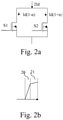
- the Fig. 2a is an example of a multi-die power module wherein two dies S1 and S2 are connected in parallel.
- the die S1 has a current equal to Id(1- ⁇ ) and the die S2 has a current equal to Id(1- ⁇ ), where ' ⁇ ' is the per-unit difference between the magnitude of commutated current.
- Fig. 2b shows the currents going through the dies when the dies switch at different timings.
- the die S2 is turned ON and during the time period noted 21, the dies S1 and S2 are turned ON.
- the input capacitance seen by the gate driver is the sum of both of the dies, and hence the switching losses are a function of these parameters given a limited gate supply voltage.
- the two commutating dies due to differing threshold voltages, begin to conduct currents at different times, leading to a mismatch of current at time 't', and oscillatory behaviour as the current tries to balance between the two dies. These oscillations then result in an increase of the Electro Magnetic Interference.
- the present invention aims at enhancing the switching speed of multi-die power modules and to increase the maximum capability of a multi-die power module by controlling switching transients for parallel-connected device without need to implement highly dynamic control.
- the present invention concerns a system comprising a multi-die power module composed of dies and a controller arranged to receive plural consecutive input patterns for turning on and off the dies of the multi-die power module, as further specified in claim 1.
- the commutation current can effectively be concentrated in a select group of dies or a single die in order to reduce oscillations and reduce the commutation time.
- the present invention concerns also a method for controlling the operation of a multi-die power module composed of groups of dies according to claim
- the system further comprises means for adjusting the number of dies according to current requirement and maximum current driving capability of the dies of the multi-die power module.
- the system comprises further means for changing, at each input, patterns for activating the dies of the multi-die power module, of at least one gate to source signal of which the rising edge and/or a falling edge is time shifted.
- the time shift can be adapted according to different parameters that influence the rising and falling time of the commutation current in the die.
- the gate to source signals of which the rising edge and/or a falling edge are time shifted are changed on a round robin basis.
- the individual dies are not overstressed over the lifetime of the power module.
- the time shift occurrences are, at a minimum, dependent of the commutations properties of the dies and are at least ten times smaller than the total conduction time of the die.
- Fig. 1 represents an example of a system for controlling the operation of a multi-die power module according to the present invention.
- the system for controlling the operation of the multi-die power module 150 uses an open loop mechanism and controls the switching time of the dies in the multi-die power module 150.
- the system for controlling the operation of the multi-die power module 150 comprises a plurality of gate drivers 102 for providing a driving signal to at least one or plural dies 105 of the multi-die power module 150.
- the system for controlling the operation of the multi-die power module 150 comprises three gate drivers 102a to 102c for controlling the operation of three groups of at least one power die.
- each group of at least one power die comprises one die, respectively noted 105a to 105c.
- the gate drivers 102a to 102 receive command signal from a controller 104 which is disclosed in reference to Fig. 3 .
- Fig. 3 represents an example of an architecture of a controller of the system for controlling the operation of a multi-die power module according to the present invention.
- the controller 104 has, for example, an architecture based on components connected together by a bus 301 and a processor 300 controlled by the program as disclosed in Fig. 6 .
- the bus 301 links the processor 200 to a read only memory ROM 302, a random access memory RAM 303 and an input/output interface I/O 305.
- the memory 303 contains registers intended to receive variables and the instructions of the program related to the algorithm as disclosed in Fig. 6 .
- the processor 300 receives command patterns from a host controller through the input/output interface 305, modifies the rising/falling edge times of the signal to be applied by the gate drivers 102 to the dies 105 and transfers them to the gate drivers 102 through the input/output interface 305.
- the input/output interface I/O 205 may be split into two interfaces, one with the host controller and one with the device for controlling the operation of a power die 102.
- the controller 104 receives an activation or load command from a host controller.
- the controller 104 interprets this activation command and provides synchronized control over the plurality of dies.
- the read only memory 302 contains instructions of the program related to the algorithm as disclosed in Fig. 6 , which are transferred, when the controller 104 is powered on, to the random access memory 303.
- Any and all steps of the algorithm described hereafter with regard to Fig. 6 may be implemented in software by execution of a set of instructions or program by a programmable computing machine, such as a PC (Personal Computer), a DSP (Digital Signal Processor) or a microcontroller; or else implemented in hardware by a machine or a dedicated component, such as an FPGA (Field-Programmable Gate Array) or an ASIC (Application-Specific Integrated Circuit).
- a programmable computing machine such as a PC (Personal Computer), a DSP (Digital Signal Processor) or a microcontroller; or else implemented in hardware by a machine or a dedicated component, such as an FPGA (Field-Programmable Gate Array) or an ASIC (Application-Specific Integrated Circuit).
- the controller 104 includes circuitry, or a device including circuitry, causing the controller 104 to perform the steps of the algorithm described hereafter with regard to Fig. 6 .
- the controller 104 may be realized, for example, by a pre-programmed CPLD (Complex Programmable Logic Device).
- CPLD Complex Programmable Logic Device
- the dies are grouped into plural groups of at least one die and the controller comprises:
- Fig. 4 represents control of the switching timing of a multi-die power module in accordance with claims 1 and 4. .
- the controller 104 receives command patterns from the host controller. Command patterns are noted 400.
- the active time i.e. the high level state, of the control patterns are comprised between 2 microseconds to 10 microseconds.
- the signal noted 410 is the signal provided to the gate driver 102a
- the signal noted 420 is the signal provided to the gate driver 102b
- the signal noted 430 is the signal provided to the gate driver 102c.
- the controller 104 delays rising edge times, advances falling edge times on a round trip basis.
- the controller 104 At first high level state of the control pattern, the controller 104 generates a high level 411 for the signal 410 by advancing the falling edge time by a predetermined value, the controller 104 generates a high level 421 for the signal 420 by delaying the rising edge time by the predetermined value and the controller 104 generates a high level 431 for the signal 430 by delaying the rising edge time by the predetermined value and by advancing the falling edge time by the predetermined value.
- the controller 104 At second high level state of the control pattern, the controller 104 generates a high level 412 for the signal 410 by delaying the rising edge time by the predetermined value, the controller 104 generates a high level 422 for the signal 420 by delaying the rising edge time by the predetermined value and by advancing the falling edge time by the predetermined value and the controller 104 generates a high level 432 for the signal 430 by advancing the falling edge time by the predetermined value.
- the controller 104 At third high level state of the control pattern, the controller 104 generates a high level 413 for the signal 410 by delaying the rising edge time by the predetermined value and by advancing the falling edge time by the predetermined value, the controller 104 generates a high level 423 for the signal 420 by advancing the falling edge time by the predetermined value and the controller 104 generates a high level 433 for the signal 430 by delaying the rising edge time by the predetermined value.
- the round robin cycle is repeated as shown by the high levels 414, 424 and 434 which are similar as the ones noted 411, 421 and 431.
- the predetermined value is for example between 10 to 50 nanoseconds which correspond to the switching of the dies 105. It has to be noted here that this value is based on the transit delay and rise/fall times of the current in the specific die used in the multi-die power module. The predetermined value is at least ten times smaller than the total conduction time of each die.
- Figs. 5a and 5c are an example of a multi-die power module wherein two dies are connected in parallel and controlled according to the present invention.
- Fig. 5a the die S1 is conducting and the die S2 is not conducting.
- Fig. 5b the die S2 is conducting and the die S 1 is not conducting.
- the present invention by delaying or advancing the rising or falling edge time, it is possible to reduce the driving capacitance, as seen by the gate drivers.
- the global losses can fall due to a decrease in current rise/fall times.
- the increase in current does not increase the losses compared to two conducting dies if the plateau voltage is small compared to the gate voltage, and thus by decreasing the input capacitance, the losses can fall due to a shortened equivalent commutation time.
- a switching loss reduction is also achieved by negating the need for larger current sharing resistors that are typically added to improve stability during commutation by increasing the current rise and fall times within the controlled multi-die power module.
- Figs. 5b and 5d show the currents going through the dies when the dies switch at different timings according to the present invention.
- the Fig. 5b shows the commuting of the die S1
- the Fig. 5d shows the commuting of the die S2.
- Fig. 6 is an example of an algorithm for controlling the switching time of the dies of a multi-power die module according to the present invention.
- the present algorithm controls a multitude of parallel connected dies by decreasing the number of dies active during a commutation event and cycles the active dies from one high level command to another.
- the present algorithm is executed for three groups of dies as an example.
- the present invention is also applicable for a fewer or greater number of groups of dies.
- a number representing the optimal number of parallel dies for each switching event is pre-loaded into the controller 104.
- the controller 104 receives the pulse width modulation command from the host controller, sets the number of active dies, and then delays the appropriate dies on the rising or turn-on event or advances the dies on the falling or turn off events to force current into the appropriate dies.
- the number of dies used in the given switching period is stored, and then for the next switching cycle, the new number of active dies is selected.
- the inactive dies are sequentially then moved to the next die in each cycle. In this manner, the active dies are cycled through to reduce the loading on the specific dies, caused by the increased current seen during commutation.
- the processor 300 determines the minimum number of dies of each group of dies. The minimum number is determined according to the current requirement and maximum current driving capability of the dies of the multi-die power module.
- the processor 300 detects a high level state of the control pattern through the interface 305.
- the processor 300 generates a high level for the signal intended to the first group of dies comprising the die 105a by advancing the falling edge time by the predetermined value, generates a high level for the signal intended to the second group of dies comprising the die 105b by delaying the rising edge time by the predetermined value and generates a high level for the signal intended to the first group of dies comprising the die 105c by delaying the rising edge time by the predetermined value and by advancing the falling edge time by the predetermined value.
- the processor 300 detects a high level state of the control pattern through the interface 305.
- the processor 300 generates a high level for the signal intended to the first group of dies comprising the die 105a by delaying the rising edge time by the predetermined value, generates a high level for the signal intended to the second group of dies comprising the die 105b by delaying the rising edge time by the predetermined value and by advancing the falling edge time by the predetermined value and generates a high level for the signal intended to the first group of dies comprising the die 105c by advancing the falling edge time by the predetermined value.
- the processor 300 detects a high level state of the control pattern through the interface 305.
- the processor 300 generates a high level for the signal intended to the first group of dies comprising the die 105a by delaying the rising edge time by the predetermined value and by advancing the falling edge time by the predetermined value, generates a high level for the signal intended to the second group of dies comprising the die 105b by advancing the falling edge time by the predetermined value and generates a high level for the signal intended to the first group of dies comprising the die 105c by delaying the rising edge time by the predetermined value.
Landscapes
- Engineering & Computer Science (AREA)
- Power Engineering (AREA)
- Power Conversion In General (AREA)
- Semiconductor Integrated Circuits (AREA)
Claims (6)
- System, das ein Mehrchip-Leistungsmodul (150) umfasst, das aus parallelgeschalteten Chips (105a, 105b, 105c) besteht, die einen einzelnen Schalter bilden, und eine Steuerung (104), die angeordnet sind, um aufeinanderfolgende Eingangsmuster zum Ein- und Ausschalten der Chips des Mehrchip-Leistungsmoduls zu empfangen, wobei die Eingangsmuster High- und Low-Level sind und Anstiegsflanken und Abfallflanken haben, dadurch gekennzeichnet, dass die Chips in eine erste, eine zweite und eine dritte Gruppe von wenigstens einem Chip gruppiert sind und dass die Steuerung zum Durchführen auf einer Round-Robin-Basis angeordnet ist:- bei einem ersten High-Level-Zustand des Eingangsmusters Vorziehen der Abfallflankenzeit des Gate-Signals für die erste Gruppe von wenigstens einem Chip um einen vorbestimmten Wert (411), Verzögern der Anstiegsflankenzeit des Gate-Signals für die zweite Gruppe von wenigstens einem Chip um den vorbestimmten Wert (421), Verzögern der Anstiegsflankenzeit des Gate-Signals für die dritte Gruppe von wenigstens einem Chip um den vorbestimmten Wert und Vorziehen der Abfallflankenzeit des Gate-Signals für die dritte Gruppe von wenigstens einem Chip um den vorbestimmten Wert (431),- bei einem zweiten High-Level-Zustand des Eingangsmusters Verzögern der Anstiegsflankenzeit des Gate-Signals für die erste Gruppe von wenigstens einem Chip um den vorbestimmten Wert (412), Verzögern der Anstiegsflankenzeit des Gate-Signals für die zweite Gruppe von wenigstens einem Chip um den vorbestimmten Wert und Vorziehen die Abfallflankenzeit des Gate-Signals für die zweite Gruppe von wenigstens einem Chip um den vorbestimmten Wert (422) und Vorziehen der Abfallflankenzeit des Gate-Signals für die dritte Gruppe von wenigstens einem Chip um den vorbestimmten Wert (432),- bei einem dritten High-Level-Zustand des Eingangsmusters Verzögern der Anstiegsflankenzeit des Gate-Signals für die erste Gruppe von wenigstens einem Chip um den vorbestimmten Wert und Vorziehen der Abfallflankenzeit des Gate-Signals für die erste Gruppe von wenigstens einem Chip um den vorbestimmten Wert (413), Vorziehen der Abfallflankenzeit des Gate-Signals für die zweite Gruppe von wenigstens einem Chip um den vorbestimmten Wert (423) und Verzögern der Anstiegsflankenzeit des Gate-Signals für die dritte Gruppe von wenigstens einem Chip um den vorbestimmten Wert (433).
- System nach Anspruch 1, dadurch gekennzeichnet, dass das System weiterhin Mittel zum Einstellen der Anzahl von Chips gemäß einem Strombedarf und einer maximalen Stromantriebsfähigkeit der Chips des Mehrchip-Leistungsmoduls umfasst.
- System nach Anspruch 1 oder 2, dadurch gekennzeichnet, dass die Zeitverschiebungsauftritte zumindest von den Kommutierungseigenschaften der Chips abhängen und wenigstens zehnmal kleiner als die gesamte Leitungszeit des Chips sind.
- Verfahren zum Steuern des Betriebs eines Mehrchip-Leistungsmoduls (150), das aus parallelgeschalteten Chips (105a, 105b, 105c) besteht, die einen einzelnen Schalter bilden, wobei die Chips in eine erste, eine zweite und eine dritter Gruppe von wenigstens einem Chip gruppiert sind, dadurch gekennzeichnet, dass das Verfahren die folgenden Schritte umfasst, die durch eine Steuerung ausgeführt werden, die zum Durchführen auf einer Round-Robin-Basis angeordnet ist:- bei einem ersten High-Level-Zustand des Eingangsmusters Vorziehen der Abfallflankenzeit des Gate-Signals für die erste Gruppe von wenigstens einem Chip um einen vorbestimmten Wert (411), Verzögern der Anstiegsflankenzeit des Gate-Signals für die zweite Gruppe von wenigstens einem Chip um den vorbestimmten Wert (421), Verzögern der Anstiegsflankenzeit des Gate-Signals für die dritte Gruppe von wenigstens einem Chip um den vorbestimmten Wert und Vorziehen der Abfallflankenzeit des Gate-Signals für die dritte Gruppe von wenigstens einem Chip um den vorbestimmten Wert (431),- bei einem zweiten High-Level-Zustand des Eingangsmusters Verzögern der Anstiegsflankenzeit des Gate-Signals für die erste Gruppe von wenigstens einem Chip um den vorbestimmten Wert (412), Verzögern der Anstiegsflankenzeit des Gate-Signals für die zweite Gruppe von wenigstens einem Chip um den vorbestimmten Wert und Vorziehen die Abfallflankenzeit des Gate-Signals für die zweite Gruppe von wenigstens einem Chip um den vorbestimmten Wert (422) und Vorziehen der Abfallflankenzeit des Gate-Signals für die dritte Gruppe von wenigstens einem Chip um den vorbestimmten Wert (432),- bei einem dritten High-Level-Zustand des Eingangsmusters Verzögern der Anstiegsflankenzeit des Gate-Signals für die erste Gruppe von wenigstens einem Chip um den vorbestimmten Wert und Vorziehen der Abfallflankenzeit des Gate-Signals für die erste Gruppe von wenigstens einem Chip um den vorbestimmten Wert (413), Vorziehen der Abfallflankenzeit des Gate-Signals für die zweite Gruppe von wenigstens einem Chip um den vorbestimmten Wert (423) und Verzögern der Anstiegsflankenzeit des Gate-Signals für die dritte Gruppe von wenigstens einem Chip um den vorbestimmten Wert (433).
- Verfahren nach Anspruch 4, dadurch gekennzeichnet, dass das Verfahren weiterhin den Schritt zum Einstellen der Anzahl von Chips gemäß einem Strombedarf und einer maximalen Stromantriebsfähigkeit der Chips des Mehrchip-Leistungsmoduls umfasst.
- Verfahren nach Anspruch 4 oder 5, dadurch gekennzeichnet, dass die Zeitverschiebungsauftritte zumindest von den Kommutierungseigenschaften der Chips abhängen und wenigstens zehnmal kleiner als die gesamte Leitungszeit des Chips sind.
Priority Applications (5)
| Application Number | Priority Date | Filing Date | Title |
|---|---|---|---|
| EP15172320.2A EP3107197B1 (de) | 2015-06-16 | 2015-06-16 | System und verfahren zur steuerung des betriebs eines mehrchip-leistungsmoduls |
| CN201680033881.4A CN107735950B (zh) | 2015-06-16 | 2016-06-15 | 包括多晶片功率模块的系统和用于控制多晶片功率模块的操作的方法 |
| PCT/JP2016/068448 WO2016204305A1 (en) | 2015-06-16 | 2016-06-15 | System comprising multi-die power module and method for controlling operation of multi-die power module |
| JP2017542923A JP6429222B2 (ja) | 2015-06-16 | 2016-06-15 | マルチダイパワーモジュールを備えるシステム及びマルチダイパワーモジュールの動作を制御する方法 |
| US15/574,632 US10367497B2 (en) | 2015-06-16 | 2016-06-15 | System comprising multi-die power and method for controlling operation of multi-die power module |
Applications Claiming Priority (1)
| Application Number | Priority Date | Filing Date | Title |
|---|---|---|---|
| EP15172320.2A EP3107197B1 (de) | 2015-06-16 | 2015-06-16 | System und verfahren zur steuerung des betriebs eines mehrchip-leistungsmoduls |
Publications (2)
| Publication Number | Publication Date |
|---|---|
| EP3107197A1 EP3107197A1 (de) | 2016-12-21 |
| EP3107197B1 true EP3107197B1 (de) | 2022-01-19 |
Family
ID=53434252
Family Applications (1)
| Application Number | Title | Priority Date | Filing Date |
|---|---|---|---|
| EP15172320.2A Not-in-force EP3107197B1 (de) | 2015-06-16 | 2015-06-16 | System und verfahren zur steuerung des betriebs eines mehrchip-leistungsmoduls |
Country Status (5)
| Country | Link |
|---|---|
| US (1) | US10367497B2 (de) |
| EP (1) | EP3107197B1 (de) |
| JP (1) | JP6429222B2 (de) |
| CN (1) | CN107735950B (de) |
| WO (1) | WO2016204305A1 (de) |
Families Citing this family (4)
| Publication number | Priority date | Publication date | Assignee | Title |
|---|---|---|---|---|
| JP6820825B2 (ja) * | 2017-11-09 | 2021-01-27 | 三菱電機株式会社 | 半導体装置及びその駆動方法 |
| CN113765339B (zh) * | 2020-06-01 | 2025-01-24 | 株式会社村田制作所 | 避免并联式半导体开关中的寄生振荡的方法及对应的装置 |
| WO2023148134A1 (de) * | 2022-02-02 | 2023-08-10 | Fronius International Gmbh | Verlustarmer gleichspannungswandler und zugehöriges ansteuerungsverfahren |
| FR3164060A1 (fr) * | 2024-07-01 | 2026-01-02 | Commissariat A L' Energie Atomique Et Aux Energies Alternatives | Dispositif à branches parallèles |
Citations (2)
| Publication number | Priority date | Publication date | Assignee | Title |
|---|---|---|---|---|
| EP0581016B1 (de) * | 1992-06-26 | 1997-12-29 | Kollmorgen Corporation | Einrichtung und Verfahren zum erzwungenen Verteilen der Schaltverluste parallelgeschalteter Transistoren |
| WO2012123027A1 (en) * | 2011-03-16 | 2012-09-20 | Abb Research Ltd | Gate control circuit, power module and associated method |
Family Cites Families (8)
| Publication number | Priority date | Publication date | Assignee | Title |
|---|---|---|---|---|
| JP2656537B2 (ja) * | 1988-04-13 | 1997-09-24 | 株式会社日立製作所 | 電力用半導体装置 |
| DE4435255A1 (de) * | 1994-10-01 | 1996-04-04 | Abb Management Ag | Verfahren zur Fehlerbehebung in einer Stromrichterschaltungsanordnung |
| DE10156963A1 (de) * | 2001-11-20 | 2003-06-05 | Fritz Frey | Schaltungsanordnung zum zuverlässigen Schalten von Stromkreisen |
| US20040103248A1 (en) * | 2002-10-08 | 2004-05-27 | Hass David T. | Advanced telecommunications processor |
| KR100595447B1 (ko) * | 2004-03-26 | 2006-07-03 | 삼성전자주식회사 | Dc-dc 컨버터 및 그 제어방법 |
| EP2154784A1 (de) * | 2008-08-16 | 2010-02-17 | SEMIKRON Elektronik GmbH & Co. KG | Anordnung mit einer Treiberschaltung und mindestens einem Leistungsschalter sowie Ansteuerverfahren hierzu |
| EP2587670A1 (de) * | 2011-10-26 | 2013-05-01 | ABB Technology AG | Steuerungskontaktantriebssystem |
| CN203675001U (zh) * | 2014-01-21 | 2014-06-25 | 唐山开诚电控设备集团有限公司 | 一种新型低功耗三电平变频器逆变单元 |
-
2015
- 2015-06-16 EP EP15172320.2A patent/EP3107197B1/de not_active Not-in-force
-
2016
- 2016-06-15 WO PCT/JP2016/068448 patent/WO2016204305A1/en not_active Ceased
- 2016-06-15 US US15/574,632 patent/US10367497B2/en not_active Expired - Fee Related
- 2016-06-15 CN CN201680033881.4A patent/CN107735950B/zh not_active Expired - Fee Related
- 2016-06-15 JP JP2017542923A patent/JP6429222B2/ja not_active Expired - Fee Related
Patent Citations (2)
| Publication number | Priority date | Publication date | Assignee | Title |
|---|---|---|---|---|
| EP0581016B1 (de) * | 1992-06-26 | 1997-12-29 | Kollmorgen Corporation | Einrichtung und Verfahren zum erzwungenen Verteilen der Schaltverluste parallelgeschalteter Transistoren |
| WO2012123027A1 (en) * | 2011-03-16 | 2012-09-20 | Abb Research Ltd | Gate control circuit, power module and associated method |
Also Published As
| Publication number | Publication date |
|---|---|
| CN107735950B (zh) | 2021-02-19 |
| US20180138901A1 (en) | 2018-05-17 |
| US10367497B2 (en) | 2019-07-30 |
| EP3107197A1 (de) | 2016-12-21 |
| WO2016204305A1 (en) | 2016-12-22 |
| CN107735950A (zh) | 2018-02-23 |
| JP2018506954A (ja) | 2018-03-08 |
| JP6429222B2 (ja) | 2018-11-28 |
Similar Documents
| Publication | Publication Date | Title |
|---|---|---|
| CN100527589C (zh) | 考虑逆变器非线性的电压源逆变器的最小损失pwm | |
| Zhang et al. | A smart gate driver IC for GaN power HEMTs with dynamic ringing suppression | |
| EP3107197B1 (de) | System und verfahren zur steuerung des betriebs eines mehrchip-leistungsmoduls | |
| US6545452B2 (en) | Method and device for controlling a power converter valve that can be turned off and has at least two series circuits | |
| JP6883450B2 (ja) | ゲート駆動装置、ゲート駆動方法、及び半導体装置 | |
| CN103855928B (zh) | 多功能数字脉冲宽度调变控制器 | |
| JP3512248B2 (ja) | 電子パワーコンバータ回路装置、およびこの装置の駆動方法 | |
| EP2276159A1 (de) | Digitaler Pulsweitenmodulator | |
| JP2017028811A (ja) | 半導体装置 | |
| EP4117182B1 (de) | Gate-treiberschaltung und leistungswandler | |
| EP3026801B1 (de) | Vorrichtung zur Steuerung des Betriebs eines Mehrchipleistungsmoduls | |
| Palmer et al. | SiC MOSFETs connected in series with active voltage control | |
| TWI784727B (zh) | 馬達驅動電路及馬達模組 | |
| JP2018505643A (ja) | マルチダイパワーモジュールを備えるシステム、及びマルチダイパワーモジュールのスイッチングを制御する方法 | |
| JP4786305B2 (ja) | インバータ | |
| Alam et al. | Operation point based optimization of switching losses with current-source gate driver for SiC-based power modules | |
| Li et al. | Dynamic gate drive for SiC power MOSFETs with sub-nanosecond timings | |
| JP7119681B2 (ja) | 信号伝達装置及び駆動装置 | |
| Obara et al. | Design and implementation of digital active gate control with variable 63-level drivability controlled by serial 4-bit signals | |
| Li et al. | How to turn off SiC MOSFET with low losses and low EMI across the full operating range | |
| Frank et al. | A Comparison of Gate Resistance and Gate Voltage Manipulation Active Gate Drivers for Silicon Carbide MOSFETs | |
| Lee et al. | Active gate control for multiple series connected SiC MOSFETs | |
| US12597919B2 (en) | Driving method and driving device for semiconductor device, and power conversion apparatus | |
| KR20200067325A (ko) | 전력용 mosfet 게이트 구동회로 | |
| CN105191109B (zh) | 功率模块 |
Legal Events
| Date | Code | Title | Description |
|---|---|---|---|
| PUAI | Public reference made under article 153(3) epc to a published international application that has entered the european phase |
Free format text: ORIGINAL CODE: 0009012 |
|
| STAA | Information on the status of an ep patent application or granted ep patent |
Free format text: STATUS: THE APPLICATION HAS BEEN PUBLISHED |
|
| AK | Designated contracting states |
Kind code of ref document: A1 Designated state(s): AL AT BE BG CH CY CZ DE DK EE ES FI FR GB GR HR HU IE IS IT LI LT LU LV MC MK MT NL NO PL PT RO RS SE SI SK SM TR |
|
| AX | Request for extension of the european patent |
Extension state: BA ME |
|
| STAA | Information on the status of an ep patent application or granted ep patent |
Free format text: STATUS: REQUEST FOR EXAMINATION WAS MADE |
|
| 17P | Request for examination filed |
Effective date: 20170620 |
|
| RBV | Designated contracting states (corrected) |
Designated state(s): AL AT BE BG CH CY CZ DE DK EE ES FI FR GB GR HR HU IE IS IT LI LT LU LV MC MK MT NL NO PL PT RO RS SE SI SK SM TR |
|
| STAA | Information on the status of an ep patent application or granted ep patent |
Free format text: STATUS: EXAMINATION IS IN PROGRESS |
|
| 17Q | First examination report despatched |
Effective date: 20170726 |
|
| GRAP | Despatch of communication of intention to grant a patent |
Free format text: ORIGINAL CODE: EPIDOSNIGR1 |
|
| STAA | Information on the status of an ep patent application or granted ep patent |
Free format text: STATUS: GRANT OF PATENT IS INTENDED |
|
| RIC1 | Information provided on ipc code assigned before grant |
Ipc: H03K 17/14 20060101ALI20210803BHEP Ipc: H03K 17/12 20060101ALI20210803BHEP Ipc: H02M 1/088 20060101AFI20210803BHEP |
|
| INTG | Intention to grant announced |
Effective date: 20210907 |
|
| GRAS | Grant fee paid |
Free format text: ORIGINAL CODE: EPIDOSNIGR3 |
|
| GRAA | (expected) grant |
Free format text: ORIGINAL CODE: 0009210 |
|
| STAA | Information on the status of an ep patent application or granted ep patent |
Free format text: STATUS: THE PATENT HAS BEEN GRANTED |
|
| AK | Designated contracting states |
Kind code of ref document: B1 Designated state(s): AL AT BE BG CH CY CZ DE DK EE ES FI FR GB GR HR HU IE IS IT LI LT LU LV MC MK MT NL NO PL PT RO RS SE SI SK SM TR |
|
| REG | Reference to a national code |
Ref country code: GB Ref legal event code: FG4D |
|
| REG | Reference to a national code |
Ref country code: CH Ref legal event code: EP |
|
| REG | Reference to a national code |
Ref country code: DE Ref legal event code: R096 Ref document number: 602015076517 Country of ref document: DE |
|
| REG | Reference to a national code |
Ref country code: AT Ref legal event code: REF Ref document number: 1464353 Country of ref document: AT Kind code of ref document: T Effective date: 20220215 |
|
| REG | Reference to a national code |
Ref country code: IE Ref legal event code: FG4D |
|
| REG | Reference to a national code |
Ref country code: LT Ref legal event code: MG9D |
|
| REG | Reference to a national code |
Ref country code: NL Ref legal event code: MP Effective date: 20220119 |
|
| REG | Reference to a national code |
Ref country code: AT Ref legal event code: MK05 Ref document number: 1464353 Country of ref document: AT Kind code of ref document: T Effective date: 20220119 |
|
| PG25 | Lapsed in a contracting state [announced via postgrant information from national office to epo] |
Ref country code: NL Free format text: LAPSE BECAUSE OF FAILURE TO SUBMIT A TRANSLATION OF THE DESCRIPTION OR TO PAY THE FEE WITHIN THE PRESCRIBED TIME-LIMIT Effective date: 20220119 |
|
| PG25 | Lapsed in a contracting state [announced via postgrant information from national office to epo] |
Ref country code: SE Free format text: LAPSE BECAUSE OF FAILURE TO SUBMIT A TRANSLATION OF THE DESCRIPTION OR TO PAY THE FEE WITHIN THE PRESCRIBED TIME-LIMIT Effective date: 20220119 Ref country code: RS Free format text: LAPSE BECAUSE OF FAILURE TO SUBMIT A TRANSLATION OF THE DESCRIPTION OR TO PAY THE FEE WITHIN THE PRESCRIBED TIME-LIMIT Effective date: 20220119 Ref country code: PT Free format text: LAPSE BECAUSE OF FAILURE TO SUBMIT A TRANSLATION OF THE DESCRIPTION OR TO PAY THE FEE WITHIN THE PRESCRIBED TIME-LIMIT Effective date: 20220519 Ref country code: NO Free format text: LAPSE BECAUSE OF FAILURE TO SUBMIT A TRANSLATION OF THE DESCRIPTION OR TO PAY THE FEE WITHIN THE PRESCRIBED TIME-LIMIT Effective date: 20220419 Ref country code: LT Free format text: LAPSE BECAUSE OF FAILURE TO SUBMIT A TRANSLATION OF THE DESCRIPTION OR TO PAY THE FEE WITHIN THE PRESCRIBED TIME-LIMIT Effective date: 20220119 Ref country code: HR Free format text: LAPSE BECAUSE OF FAILURE TO SUBMIT A TRANSLATION OF THE DESCRIPTION OR TO PAY THE FEE WITHIN THE PRESCRIBED TIME-LIMIT Effective date: 20220119 Ref country code: ES Free format text: LAPSE BECAUSE OF FAILURE TO SUBMIT A TRANSLATION OF THE DESCRIPTION OR TO PAY THE FEE WITHIN THE PRESCRIBED TIME-LIMIT Effective date: 20220119 Ref country code: BG Free format text: LAPSE BECAUSE OF FAILURE TO SUBMIT A TRANSLATION OF THE DESCRIPTION OR TO PAY THE FEE WITHIN THE PRESCRIBED TIME-LIMIT Effective date: 20220419 |
|
| PG25 | Lapsed in a contracting state [announced via postgrant information from national office to epo] |
Ref country code: PL Free format text: LAPSE BECAUSE OF FAILURE TO SUBMIT A TRANSLATION OF THE DESCRIPTION OR TO PAY THE FEE WITHIN THE PRESCRIBED TIME-LIMIT Effective date: 20220119 Ref country code: LV Free format text: LAPSE BECAUSE OF FAILURE TO SUBMIT A TRANSLATION OF THE DESCRIPTION OR TO PAY THE FEE WITHIN THE PRESCRIBED TIME-LIMIT Effective date: 20220119 Ref country code: GR Free format text: LAPSE BECAUSE OF FAILURE TO SUBMIT A TRANSLATION OF THE DESCRIPTION OR TO PAY THE FEE WITHIN THE PRESCRIBED TIME-LIMIT Effective date: 20220420 Ref country code: FI Free format text: LAPSE BECAUSE OF FAILURE TO SUBMIT A TRANSLATION OF THE DESCRIPTION OR TO PAY THE FEE WITHIN THE PRESCRIBED TIME-LIMIT Effective date: 20220119 Ref country code: AT Free format text: LAPSE BECAUSE OF FAILURE TO SUBMIT A TRANSLATION OF THE DESCRIPTION OR TO PAY THE FEE WITHIN THE PRESCRIBED TIME-LIMIT Effective date: 20220119 |
|
| PG25 | Lapsed in a contracting state [announced via postgrant information from national office to epo] |
Ref country code: IS Free format text: LAPSE BECAUSE OF FAILURE TO SUBMIT A TRANSLATION OF THE DESCRIPTION OR TO PAY THE FEE WITHIN THE PRESCRIBED TIME-LIMIT Effective date: 20220519 |
|
| REG | Reference to a national code |
Ref country code: DE Ref legal event code: R097 Ref document number: 602015076517 Country of ref document: DE |
|
| PG25 | Lapsed in a contracting state [announced via postgrant information from national office to epo] |
Ref country code: SM Free format text: LAPSE BECAUSE OF FAILURE TO SUBMIT A TRANSLATION OF THE DESCRIPTION OR TO PAY THE FEE WITHIN THE PRESCRIBED TIME-LIMIT Effective date: 20220119 Ref country code: SK Free format text: LAPSE BECAUSE OF FAILURE TO SUBMIT A TRANSLATION OF THE DESCRIPTION OR TO PAY THE FEE WITHIN THE PRESCRIBED TIME-LIMIT Effective date: 20220119 Ref country code: RO Free format text: LAPSE BECAUSE OF FAILURE TO SUBMIT A TRANSLATION OF THE DESCRIPTION OR TO PAY THE FEE WITHIN THE PRESCRIBED TIME-LIMIT Effective date: 20220119 Ref country code: EE Free format text: LAPSE BECAUSE OF FAILURE TO SUBMIT A TRANSLATION OF THE DESCRIPTION OR TO PAY THE FEE WITHIN THE PRESCRIBED TIME-LIMIT Effective date: 20220119 Ref country code: DK Free format text: LAPSE BECAUSE OF FAILURE TO SUBMIT A TRANSLATION OF THE DESCRIPTION OR TO PAY THE FEE WITHIN THE PRESCRIBED TIME-LIMIT Effective date: 20220119 Ref country code: CZ Free format text: LAPSE BECAUSE OF FAILURE TO SUBMIT A TRANSLATION OF THE DESCRIPTION OR TO PAY THE FEE WITHIN THE PRESCRIBED TIME-LIMIT Effective date: 20220119 |
|
| PLBE | No opposition filed within time limit |
Free format text: ORIGINAL CODE: 0009261 |
|
| STAA | Information on the status of an ep patent application or granted ep patent |
Free format text: STATUS: NO OPPOSITION FILED WITHIN TIME LIMIT |
|
| PG25 | Lapsed in a contracting state [announced via postgrant information from national office to epo] |
Ref country code: AL Free format text: LAPSE BECAUSE OF FAILURE TO SUBMIT A TRANSLATION OF THE DESCRIPTION OR TO PAY THE FEE WITHIN THE PRESCRIBED TIME-LIMIT Effective date: 20220119 |
|
| 26N | No opposition filed |
Effective date: 20221020 |
|
| PG25 | Lapsed in a contracting state [announced via postgrant information from national office to epo] |
Ref country code: MC Free format text: LAPSE BECAUSE OF FAILURE TO SUBMIT A TRANSLATION OF THE DESCRIPTION OR TO PAY THE FEE WITHIN THE PRESCRIBED TIME-LIMIT Effective date: 20220119 |
|
| REG | Reference to a national code |
Ref country code: CH Ref legal event code: PL |
|
| REG | Reference to a national code |
Ref country code: BE Ref legal event code: MM Effective date: 20220630 |
|
| PG25 | Lapsed in a contracting state [announced via postgrant information from national office to epo] |
Ref country code: SI Free format text: LAPSE BECAUSE OF FAILURE TO SUBMIT A TRANSLATION OF THE DESCRIPTION OR TO PAY THE FEE WITHIN THE PRESCRIBED TIME-LIMIT Effective date: 20220119 |
|
| PG25 | Lapsed in a contracting state [announced via postgrant information from national office to epo] |
Ref country code: LU Free format text: LAPSE BECAUSE OF NON-PAYMENT OF DUE FEES Effective date: 20220616 Ref country code: LI Free format text: LAPSE BECAUSE OF NON-PAYMENT OF DUE FEES Effective date: 20220630 Ref country code: IE Free format text: LAPSE BECAUSE OF NON-PAYMENT OF DUE FEES Effective date: 20220616 Ref country code: CH Free format text: LAPSE BECAUSE OF NON-PAYMENT OF DUE FEES Effective date: 20220630 |
|
| PG25 | Lapsed in a contracting state [announced via postgrant information from national office to epo] |
Ref country code: BE Free format text: LAPSE BECAUSE OF NON-PAYMENT OF DUE FEES Effective date: 20220630 |
|
| P01 | Opt-out of the competence of the unified patent court (upc) registered |
Effective date: 20230512 |
|
| PG25 | Lapsed in a contracting state [announced via postgrant information from national office to epo] |
Ref country code: IT Free format text: LAPSE BECAUSE OF FAILURE TO SUBMIT A TRANSLATION OF THE DESCRIPTION OR TO PAY THE FEE WITHIN THE PRESCRIBED TIME-LIMIT Effective date: 20220119 |
|
| PGFP | Annual fee paid to national office [announced via postgrant information from national office to epo] |
Ref country code: FR Payment date: 20230628 Year of fee payment: 9 Ref country code: DE Payment date: 20230620 Year of fee payment: 9 |
|
| PGFP | Annual fee paid to national office [announced via postgrant information from national office to epo] |
Ref country code: GB Payment date: 20230622 Year of fee payment: 9 |
|
| REG | Reference to a national code |
Ref country code: DE Ref legal event code: R082 Ref document number: 602015076517 Country of ref document: DE Representative=s name: PUSCHMANN BORCHERT KAISER KLETTNER PATENTANWAE, DE |
|
| PG25 | Lapsed in a contracting state [announced via postgrant information from national office to epo] |
Ref country code: HU Free format text: LAPSE BECAUSE OF FAILURE TO SUBMIT A TRANSLATION OF THE DESCRIPTION OR TO PAY THE FEE WITHIN THE PRESCRIBED TIME-LIMIT; INVALID AB INITIO Effective date: 20150616 |
|
| PG25 | Lapsed in a contracting state [announced via postgrant information from national office to epo] |
Ref country code: MK Free format text: LAPSE BECAUSE OF FAILURE TO SUBMIT A TRANSLATION OF THE DESCRIPTION OR TO PAY THE FEE WITHIN THE PRESCRIBED TIME-LIMIT Effective date: 20220119 Ref country code: CY Free format text: LAPSE BECAUSE OF FAILURE TO SUBMIT A TRANSLATION OF THE DESCRIPTION OR TO PAY THE FEE WITHIN THE PRESCRIBED TIME-LIMIT Effective date: 20220119 |
|
| PG25 | Lapsed in a contracting state [announced via postgrant information from national office to epo] |
Ref country code: TR Free format text: LAPSE BECAUSE OF FAILURE TO SUBMIT A TRANSLATION OF THE DESCRIPTION OR TO PAY THE FEE WITHIN THE PRESCRIBED TIME-LIMIT Effective date: 20220119 |
|
| PG25 | Lapsed in a contracting state [announced via postgrant information from national office to epo] |
Ref country code: MT Free format text: LAPSE BECAUSE OF FAILURE TO SUBMIT A TRANSLATION OF THE DESCRIPTION OR TO PAY THE FEE WITHIN THE PRESCRIBED TIME-LIMIT Effective date: 20220119 |
|
| REG | Reference to a national code |
Ref country code: DE Ref legal event code: R119 Ref document number: 602015076517 Country of ref document: DE |
|
| GBPC | Gb: european patent ceased through non-payment of renewal fee |
Effective date: 20240616 |
|
| PG25 | Lapsed in a contracting state [announced via postgrant information from national office to epo] |
Ref country code: DE Free format text: LAPSE BECAUSE OF NON-PAYMENT OF DUE FEES Effective date: 20250101 |
|
| PG25 | Lapsed in a contracting state [announced via postgrant information from national office to epo] |
Ref country code: FR Free format text: LAPSE BECAUSE OF NON-PAYMENT OF DUE FEES Effective date: 20240630 |
|
| PG25 | Lapsed in a contracting state [announced via postgrant information from national office to epo] |
Ref country code: GB Free format text: LAPSE BECAUSE OF NON-PAYMENT OF DUE FEES Effective date: 20240616 |