EP3109681B1 - Optische anordnung und optisches modul - Google Patents
Optische anordnung und optisches modul Download PDFInfo
- Publication number
- EP3109681B1 EP3109681B1 EP16176153.1A EP16176153A EP3109681B1 EP 3109681 B1 EP3109681 B1 EP 3109681B1 EP 16176153 A EP16176153 A EP 16176153A EP 3109681 B1 EP3109681 B1 EP 3109681B1
- Authority
- EP
- European Patent Office
- Prior art keywords
- incident rays
- optical
- total reflection
- disposed
- reflection device
- Prior art date
- Legal status (The legal status is an assumption and is not a legal conclusion. Google has not performed a legal analysis and makes no representation as to the accuracy of the status listed.)
- Active
Links
Images

Classifications
-
- G—PHYSICS
- G02—OPTICS
- G02B—OPTICAL ELEMENTS, SYSTEMS OR APPARATUS
- G02B6/00—Light guides; Structural details of arrangements comprising light guides and other optical elements, e.g. couplings
- G02B6/24—Coupling light guides
- G02B6/42—Coupling light guides with opto-electronic elements
- G02B6/4201—Packages, e.g. shape, construction, internal or external details
- G02B6/4204—Packages, e.g. shape, construction, internal or external details the coupling comprising intermediate optical elements, e.g. lenses, holograms
- G02B6/4214—Packages, e.g. shape, construction, internal or external details the coupling comprising intermediate optical elements, e.g. lenses, holograms the intermediate optical element having redirecting reflective means, e.g. mirrors, prisms for deflecting the radiation from horizontal to down- or upward direction toward a device
-
- G—PHYSICS
- G02—OPTICS
- G02B—OPTICAL ELEMENTS, SYSTEMS OR APPARATUS
- G02B6/00—Light guides; Structural details of arrangements comprising light guides and other optical elements, e.g. couplings
- G02B6/24—Coupling light guides
- G02B6/42—Coupling light guides with opto-electronic elements
- G02B6/4201—Packages, e.g. shape, construction, internal or external details
- G02B6/4204—Packages, e.g. shape, construction, internal or external details the coupling comprising intermediate optical elements, e.g. lenses, holograms
-
- G—PHYSICS
- G02—OPTICS
- G02B—OPTICAL ELEMENTS, SYSTEMS OR APPARATUS
- G02B6/00—Light guides; Structural details of arrangements comprising light guides and other optical elements, e.g. couplings
- G02B6/24—Coupling light guides
- G02B6/42—Coupling light guides with opto-electronic elements
- G02B6/4201—Packages, e.g. shape, construction, internal or external details
- G02B6/4246—Bidirectionally operating package structures
-
- G—PHYSICS
- G02—OPTICS
- G02B—OPTICAL ELEMENTS, SYSTEMS OR APPARATUS
- G02B6/00—Light guides; Structural details of arrangements comprising light guides and other optical elements, e.g. couplings
- G02B6/24—Coupling light guides
- G02B6/42—Coupling light guides with opto-electronic elements
- G02B6/4201—Packages, e.g. shape, construction, internal or external details
- G02B6/4286—Optical modules with optical power monitoring
-
- G—PHYSICS
- G02—OPTICS
- G02B—OPTICAL ELEMENTS, SYSTEMS OR APPARATUS
- G02B6/00—Light guides; Structural details of arrangements comprising light guides and other optical elements, e.g. couplings
- G02B6/24—Coupling light guides
- G02B6/26—Optical coupling means
- G02B6/28—Optical coupling means having data bus means, i.e. plural waveguides interconnected and providing an inherently bidirectional system by mixing and splitting signals
- G02B6/293—Optical coupling means having data bus means, i.e. plural waveguides interconnected and providing an inherently bidirectional system by mixing and splitting signals with wavelength selective means
- G02B6/29346—Optical coupling means having data bus means, i.e. plural waveguides interconnected and providing an inherently bidirectional system by mixing and splitting signals with wavelength selective means operating by wave or beam interference
- G02B6/29361—Interference filters, e.g. multilayer coatings, thin film filters, dichroic splitters or mirrors based on multilayers, WDM filters
-
- G—PHYSICS
- G02—OPTICS
- G02B—OPTICAL ELEMENTS, SYSTEMS OR APPARATUS
- G02B6/00—Light guides; Structural details of arrangements comprising light guides and other optical elements, e.g. couplings
- G02B6/24—Coupling light guides
- G02B6/42—Coupling light guides with opto-electronic elements
- G02B6/4292—Coupling light guides with opto-electronic elements the light guide being disconnectable from the opto-electronic element, e.g. mutually self aligning arrangements
Definitions
- Embodiments of the present invention relate to optoelectronic technologies, and in particular, to an optical assembly and an optical module.
- an optical module for which parallel cables are used becomes a solution of further improving receiving and sending efficiency, for example, a protocol module such as a quad SFP (QSFP) interface based on a multiple-fiber push-on/pull-off (MPO) interface, and a 120 GB/s 12x Small Form-factor Pluggable (CXP) interface.
- QSFP quad SFP
- MPO multiple-fiber push-on/pull-off
- CXP Small Form-factor Pluggable
- US 2015/0086165A1 refers to an optical receptacle and optical module provided with the same.
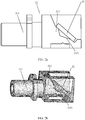
- FIG. 1a is a schematic diagram of an optical module packaged by means of the COB
- FIG. 1b is a schematic diagram of a commonly used molded plastic piece. As shown in FIG. 1a and FIG.
- a manner in which the optical module is packaged by means of the COB is directly fastening an optical chip (for example, a laser or a PD) on a printed circuit board (PCB) by using an integrally formed molded plastic piece, where two prisms are disposed in the molded plastic piece, light from a laser 102 is collimated by a lens 119 and then is turned horizontal by a reflection surface 111, and after travelling through a part of an optical path, a part of rays are reflected by a disposed clearance surface 113 to a monitor photodetector (MPD) for energy testing.
- MPD monitor photodetector
- Embodiments of the present invention provide an optical assembly and an optical module, so as to resolve a problem that when a COB technology is used for an optical module, a length of a molded plastic piece is caused to be relatively long because of an optical path, making it difficult to implement miniaturization of the optical module.
- a first aspect of the present invention provides an optical assembly, according to claim 1.
- the optical assembly comprises:
- a first lens and a second lens are further disposed in the light processing portion, where the first lens is disposed at a position from which the incident rays enter an optical path, and is configured to refract dispersed incident rays to parallel incident rays; and the second lens is disposed on an optical path that is obtained after reflection by the total reflection device, and is configured to focus the incident rays reflected by the total reflection device.
- the total reflection device includes a reflection sheet or a total reflection profile.
- an angle range of a first included angle between a reflective surface of the total reflection device and the incident rays is 30 degrees to 60 degrees.
- the first included angle is 45 degrees.
- an angle range of a second included angle between a plane on which the light splitting surface is located and the incident rays is 45 degrees to 90 degrees.
- the main body is in an integrally formed structure.
- a second aspect of the present invention provides an optical module, including: an optical module circuit, a substrate, and an optical assembly, where the optical module circuit includes a monitor photodetector MPD, and the optical module circuit and the optical assembly are disposed on the substrate; and the optical assembly includes a main body and a total reflection device, where the main body includes a fiber connection portion and a light processing portion, where the fiber connection portion is connected to the light processing portion, the fiber connection portion is connected to an external fiber, a light splitting surface is disposed in the light processing portion and is in contact with the total reflection device, the total reflection device is disposed in the light processing portion, and the light splitting surface is configured to reflect a part of incident rays to the MPD, and transmit the other part of the incident rays; and the total reflection device is configured to reflect, to the fiber connected to the fiber connection portion, the incident rays transmitted by the light splitting surface.
- a first lens and a second lens are further disposed in the light processing portion, where the first lens is disposed at a position from which the incident rays enter an optical path, and is configured to refract dispersed incident rays to parallel incident rays; and the second lens is disposed on an optical path that is obtained after reflection by the total reflection device, and is configured to focus the incident rays reflected by the total reflection device.
- the optical module circuit further includes a laser, where the laser is configured to generate the incident rays.
- the optical module circuit further includes a photodetector (PD), where the light splitting surface is configured to reflect received rays to the PD.
- PD photodetector
- a total reflection device is directly disposed in a light processing portion, and a light splitting surface is disposed to transmit a part of incident rays to the total reflection device, where the incident rays are reflected to a connected fiber by the total reflection device, and the light splitting surface may directly reflect a small part of the incident rays to an MPD for testing.
- an optical path is relatively short, and package can be performed by means of a COB, thereby decreasing a size of the optical assembly, and implementing miniaturization of the optical module to which the optical assembly is applied.
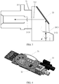
- FIG. 2a is a front view of a structure of Embodiment 1 of an optical assembly according to the present invention
- FIG. 2b is a 3D diagram of a structure of Embodiment 1 of an optical assembly according to the present invention. As shown in FIG. 2a and FIG.
- the optical assembly includes a main body 21 and a total reflection device 22, where the main body 21 includes a fiber connection portion 211 and a light processing portion 212, where the fiber connection portion 211 is connected to the light processing portion 212, and the fiber connection portion 211 is connected to an external fiber; a light splitting surface 2121 is disposed in the light processing portion 212, and is in contact with the total reflection device, where the light splitting surface 2121 is configured to reflect a part of incident rays to a monitor photodetector (English: Monitor Photo Detector, MPD for short), and transmit the other part of the incident rays; and the total reflection device 22 is disposed in the light processing portion 212, configured to reflect, to the fiber connected to the fiber connection portion 211, the incident rays transmitted by the light splitting surface 2121.
- a monitor photodetector International: Monitor Photo Detector, MPD for short
- the total reflection device 22 is disposed on the main body 21, so that incident rays can be reflected, and the light processing portion 212 is configured to process the incident rays.
- the light splitting surface 2121 is disposed by means of a Fresnel reflection effect of a sloping surface, and a smooth sloping surface, that is, the light splitting surface 2121, is formed in the light processing portion 212 of the main body 21 by hollowing an optical path along which the incident rays are input. Most incident rays may be transmitted by the sloping surface. Because of the intrinsic Fresnel reflection effect, a small part of the incident rays are reflected to the disposed MPD, and a photon-generated current is generated, which may reflect a value of an output optical power.
- both a key chip and optical chip (for example, a laser) are placed on a substrate, and then the optical assembly is packaged at a proper position by using a COB technology.
- a total reflection device is directly disposed in a light processing portion, and a light splitting surface is disposed to transmit a part of incident rays to the total reflection device, where the incident rays are reflected to a connected fiber by the total reflection device, and the light splitting surface may directly reflect a small part of the incident rays to an MPD for testing.
- an optical path is relatively short, and package can be performed by means of a COB, thereby decreasing a size of the optical assembly, and implementing miniaturization of an optical module to which the optical assembly is applied.
- FIG. 3 is a schematic sectional view of Embodiment 2 of an optical assembly not according to the present invention.
- a first lens 2122 and a second lens 2123 are further disposed in the light processing portion 212 of the optical assembly, where the first lens 2122 is disposed at a position from which the incident rays enter an optical path, and is configured to refract dispersed incident rays to parallel incident rays; and the second lens 2123 is disposed on an optical path that is obtained after reflection by the total reflection device 22, and is configured to focus the incident rays reflected by the total reflection device.
- the total reflection device 22 includes a reflection sheet or a total reflection profile, or may be another device having a total reflection function.
- an angle range of a first included angle between a reflective surface of the total reflection device and the incident rays is 30 degrees to 60 degrees. As long as the incident rays can be reflected to the fiber connected to the fiber connection portion, a specific value of the first included angle is not limited in this solution.
- the first included angle may be 45 degrees.
- the incident rays when the incident rays are input in a direction perpendicular to a horizontal direction in the figure, the incident rays are refracted by the first lens 2122 into parallel rays, and are transmitted by the light splitting surface 2121 to the reflective surface of the optical reflection device; if the first included angle is 45 degrees, the incident rays may be precisely reflected to the rayconnected to the ray connection portion 211 that is parallel to a horizontal plane.
- an angle range of a second included angle between a plane on which the light splitting surface 2121 is located and the incident rays is 45 degrees to 90 degrees. That is, as a position shown in FIG. 3 , an included angle between the light splitting surface 2121 and the horizontal plane is less than 45 degrees.
- a specific value of the second included angle is not limited in this application, as long as a small part of the incident rays that are reflected by the light splitting surface can be transmitted to the MPD.
- the main body is an injection molded part in an integrally formed structure.
- a transmit optical path when dispersed rays are input to a plastic molded part, the rays are turned into parallel rays by the first lens.
- most parallel rays are transmitted by the light splitting surface, and then are transmitted to the fiber after being reflected by the total reflection device and being focused once by the second lens.
- a small part of the incident rays that are not transmitted by the light splitting surface and are reflected by the light splitting surface are reflected to the MPD for testing, where the light splitting surface is disposed by means of a Fresnel reflection effect of a sloping surface. Because of the intrinsic Fresnel reflection effect, a small part of the rays are reflected to the MPD, and a photon-generated current is generated.
- a value of the current may reflect a value of an output optical power.
- a total reflection device is directly disposed in a light processing portion, and a light splitting surface is disposed to transmit a part of incident rays to the total reflection device, where the incident rays are reflected to a connected fiber by the total reflection device, and the light splitting surface may directly reflect a small part of the incident rays to an MPD for testing.
- an optical path is relatively short, and package can be performed by means of a COB, thereby decreasing a size of the optical assembly, and implementing miniaturization of an optical module to which the optical assembly is applied.
- a first lens and a second lens are disposed to focus rays, improving a processing effect of the rays.
- FIG. 4 is a schematic structural diagram of an Embodiment of an optical module according to the present invention.
- the optical module includes: an optical module circuit 31, a substrate 32, and an optical assembly 33, where the optical module circuit 31 includes an MPD, and the optical module circuit 31 and the optical assembly 33 are disposed on the substrate 32; and the optical assembly 33 includes a main body and a total reflection device, where the main body includes a fiber connection portion and a light processing portion, where the fiber connection portion is connected to the light processing portion, the fiber connection portion is connected to an external fiber, a light splitting surface is disposed in the light processing portion and is in contact with the total reflection device, and the total reflection device is disposed in the light processing portion, where if the optical assembly is applied to a transmit optical path, the light splitting surface is configured to reflect a part of incident rays to the MPD, and transmit the other part of the incident rays; and the total reflection device is configured to reflect, to the fiber connected to the fiber connection portion, the incident rays transmitted by the
- the light processing portion is configured to process the incident rays
- the optical assembly 33 is the optical assembly shown in FIG. 2 .
- a first lens and a second lens are further disposed in the light processing portion, where the first lens is disposed at a position from which the incident rays enter an optical path, and is configured to refract dispersed incident rays to parallel incident rays; and the second lens is disposed on an optical path that is obtained after reflection by the total reflection device, and is configured to focus the incident rays reflected by the total reflection device.
- the optical module circuit 31 further includes a laser, where the laser is configured to generate the incident rays.
- the substrate 32 which may be a PCB, a flexible substrate, a ceramic substrate, or an organic substrate.
- the optical assembly 33 in this application may be effectively applied to a pluggable module, and an application example of the pluggable module is a small form-factor pluggable (English: Small Form-factor Pluggable, SFP for short) optical module shown in FIG. 4 .
- the optical assembly 33 may be directly placed on a PCB in the SFP, and directly externally connected to an LC plug, and internally connected to the laser or a receiver chip.
- the laser and a driver or the receiver chip and a trans-impedance-amplifier (English: trans-impedance-amplifier, TIA for short)) in a transmit part are placed under the main body of the optical assembly and on the module PCB.
- a board on which the module is located inputs an electrical signal to the driver by using an electrical interface of the module, and the driver drives the laser after receiving the signal, so that the laser sends an optical signal.
- a path on a receive side is precisely reverse.
- an LC fiber sends an optical chip, which is transferred to the optical assembly part in this application, and separately output to the receiver chip in a photodetector (PD).
- PD photodetector
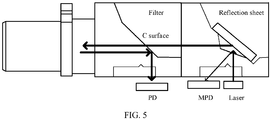
- FIG. 5 is a schematic diagram of an optical path in an embodiment of an optical module according to the present invention.
- the optical assembly 33 not only may be applied to a transmit optical path, but also may be applied to a receive optical path. If the optical assembly 33 is applied to the receive optical path, the optical module circuit further includes a PD, where the light splitting surface is configured to reflect received rays to the PD.
- the optical assembly may be further effectively applied to a module, for example, a cascaded wavelength multiplexing scenario.
- a module for example, a cascaded wavelength multiplexing scenario.
- transmitted rays and received rays have different wavelengths, and a filter is designed to perform transmission for one wavelength, and perform reflection for another wavelength, thereby implementing a BiDi transmission function.
- the rays are turned into parallel rays by a curved lens.
- the parallel rays are reflected by a reflection sheet, then are transmitted by the filter, and are input to a fiber after being focused once by a lens.
- the rays output by the fiber are reflected downward by the light splitting surface according to a total reflection effect, and are input to the PD after being focused once by the lens.
- optical assembly of this application includes a reverse design of receiving and transmission, for example, positions of the laser and the PD are exchanged, and the C surface is turned into a sloping surface, where a same principle is used.
- an improved optical module is applied to a transmit optical path or a receive optical path, a total reflection device is directly disposed in a light processing portion, and a light splitting surface is disposed to transmit a part of incident rays to the total reflection device, where the incident rays are reflected to a connected fiber by the total reflection device, and the light splitting surface may directly reflect a small part of the incident rays to an MPD for testing.
- an optical path is relatively short, and package can be performed by means of a COB, thereby decreasing a size of an optical assembly, and implementing miniaturization of the optical module to which the optical assembly is applied.
- a transmit optical power monitoring function is integrated, which can implement a module digital monitoring function, and can implement a wavelength division multiplexing function by means of multistage cascading.
Landscapes
- Physics & Mathematics (AREA)
- General Physics & Mathematics (AREA)
- Optics & Photonics (AREA)
- Optical Couplings Of Light Guides (AREA)
Claims (11)
- Optische Baugruppe, wobei die Baugruppe folgendes umfasst: einen Hauptkörper (21) und eine Totalreflexionsvorrichtung (22), wobei
der Hauptkörper (21) einen ersten Faserverbindungsteil (211) und einen Lichtverarbeitungsteil (212) umfasst, wobei der Faserverbindungsteil (211) mit dem Lichtverarbeitungsteil (212) verbunden ist;
der Faserverbindungsteil (211) mit einer externen Faser verbunden ist; und
eine Lichtteilungsoberfläche (2121) in dem Lichtverarbeitungsteil (212) angeordnet ist, wobei die Lichtteilungsoberfläche (2121) zum Reflektieren eines Teils von einfallenden Strahlen zu einem Überwachungsfotodetektor MPD und Transmittieren des anderen Teils der einfallenden Strahlen konfiguriert ist; und
die Totalreflexionsvorrichtung (22) in dem Lichtverarbeitungsteil (212) angeordnet ist, zum Reflektieren der einfallenden Strahlen, die durch die Lichtteilungsoberfläche (2121) transmittiert werden, zu der Faser, die mit dem Faserverbindungsteil (211) verbunden ist, konfiguriert ist, dadurch gekennzeichnet, dass
sich die Lichtteilungsoberfläche (2121) in Kontakt mit der Totalreflexionsvorrichtung (22) befindet. - Optische Baugruppe nach Anspruch 1, wobei eine erste Linse und eine zweite Linse ferner in dem Lichtverarbeitungsteil angeordnet sind, wobei die erste Linse bei einer Position angeordnet ist, von der die einfallenden Strahlen in einen optischen Pfad eintreten, und dazu konfiguriert ist, ein zerstreute einfallende Strahlen zu parallelen einfallenden Strahlen zu brechen; und wobei die zweite Linse in einem optischen Pfad angeordnet ist, der nach einer Reflexion durch die Totalreflexionsvorrichtung erhalten wird, und dazu konfiguriert ist, die einfallenden Strahlen, die durch die Totalreflexionsvorrichtung reflektiert werden, zu fokussieren.
- Optische Baugruppe nach Anspruch 1 oder 2, wobei die Totalreflexionsvorrichtung eine Reflexionsplatte oder ein Totalreflexionsprofil umfasst.
- Optische Baugruppe nach Anspruch 3, wobei ein Winkelbereich des ersten eingeschlossenen Winkels zwischen einer reflektierenden Oberfläche der Totalreflexionsvorrichtung und den einfallenden Strahlen 30 Grad bis 60 Grad beträgt.
- Optische Baugruppe nach Anspruch 4, wobei der erste eingeschlossene Winkel 45 Grad beträgt.
- Optische Baugruppe nach einem der Ansprüche 1 bis 5, wobei ein Winkelbereich eines zweiten eingeschlossenen Winkels zwischen einer Ebene, auf der sich die Lichtteilungsoberfläche befindet, und den einfallenden Strahlen 45 Grad bis 90 Grad beträgt.
- Optische Baugruppe nach einem der Ansprüche 1 bis 6, wobei sich der Hauptkörper in einer integral gebildeten Struktur befindet.
- Optisches Modul, wobei das Modul Folgendes umfasst: einen Optikmodulschaltkreis, ein Substrat und eine optische Baugruppe nach Anspruch 1, wobei der Optikmodulschaltkreis einen Überwachungsfotodetektor MPD umfasst und der Optikmodulschaltkreis und die optische Baugruppe auf dem Substrat angeordnet sind.
- Optisches Modul nach Anspruch 8, wobei eine erste Linse und eine zweite Linse ferner in dem Lichtverarbeitungsteil angeordnet sind, wobei die erste Linse bei einer Position angeordnet ist, von der die einfallenden Strahlen in einen optischen Pfad eintreten, und dazu konfiguriert ist, zerstreute einfallende Strahlen zu parallelen einfallenden Strahlen zu brechen; und wobei die zweite Linse in einem optischen Pfad angeordnet ist, der nach einer Reflexion durch die Totalreflexionsvorrichtung erhalten wird, und dazu konfiguriert ist, die einfallenden Strahlen, die durch die Totalreflexionsvorrichtung reflektiert werden, zu fokussieren.
- Optisches Modul nach Anspruch 8 oder 9, wobei der Optikmodulschaltkreis ferner einen Laser umfasst, wobei der Laser dazu konfiguriert ist, die einfallenden Strahlen zu erzeugen.
- Optisches Modul nach einem der Ansprüche 8 bis 10, wobei der Optikmodulschaltkreis ferner einen Fotodetektor PD umfasst, wobei die Lichtteilungsoberfläche dazu konfiguriert ist, empfangene Strahlen zu dem PD zu reflektieren.
Applications Claiming Priority (1)
| Application Number | Priority Date | Filing Date | Title |
|---|---|---|---|
| CN201510364009.5A CN106324771B (zh) | 2015-06-26 | 2015-06-26 | 光学组件和光模块 |
Publications (2)
| Publication Number | Publication Date |
|---|---|
| EP3109681A1 EP3109681A1 (de) | 2016-12-28 |
| EP3109681B1 true EP3109681B1 (de) | 2019-08-07 |
Family
ID=56235698
Family Applications (1)
| Application Number | Title | Priority Date | Filing Date |
|---|---|---|---|
| EP16176153.1A Active EP3109681B1 (de) | 2015-06-26 | 2016-06-24 | Optische anordnung und optisches modul |
Country Status (2)
| Country | Link |
|---|---|
| EP (1) | EP3109681B1 (de) |
| CN (1) | CN106324771B (de) |
Families Citing this family (11)
| Publication number | Priority date | Publication date | Assignee | Title |
|---|---|---|---|---|
| CN107479149B (zh) * | 2017-09-08 | 2019-06-21 | 峻立科技股份有限公司 | 具有监控分光路径的光学元件 |
| CN111868590B (zh) * | 2018-03-15 | 2021-10-22 | 华为技术有限公司 | 收发光器件、光模块及通讯设备 |
| CN108919433B (zh) * | 2018-07-12 | 2020-01-17 | 青岛海信宽带多媒体技术有限公司 | 一种光模块 |
| US11025030B2 (en) | 2018-07-12 | 2021-06-01 | Hisense Broadband Multimedia Technologies Co., Ltd. | Optical module |
| CN109752802A (zh) * | 2019-01-29 | 2019-05-14 | 武汉联特科技有限公司 | 多路波分复用光接收组件以及光模块 |
| CN111856661A (zh) * | 2019-04-30 | 2020-10-30 | 讯芯电子科技(中山)有限公司 | 光通信模块 |
| CN112099159A (zh) * | 2019-06-17 | 2020-12-18 | 青岛海信宽带多媒体技术有限公司 | 一种光模块 |
| CN116068700A (zh) * | 2021-11-01 | 2023-05-05 | 华为技术有限公司 | 波分复用装置 |
| CN119156558A (zh) * | 2023-04-14 | 2024-12-17 | Ii-Vi特拉华有限公司 | 用于液体浸入式冷却的光电装置 |
| CN117111227A (zh) * | 2023-06-30 | 2023-11-24 | 山东大学 | 一种光模块 |
| CN117233903A (zh) * | 2023-09-28 | 2023-12-15 | 四川华岭光子科技有限公司 | 基于光通信cob bidi的单纤双向光路模块及应用方法 |
Citations (1)
| Publication number | Priority date | Publication date | Assignee | Title |
|---|---|---|---|---|
| CN104597576A (zh) * | 2015-01-19 | 2015-05-06 | 武汉锐奥特科技有限公司 | 用在并行光模块上的带发射光功率监控的注塑光学结构 |
Family Cites Families (7)
| Publication number | Priority date | Publication date | Assignee | Title |
|---|---|---|---|---|
| DE50111575D1 (de) * | 2001-09-14 | 2007-01-11 | Infineon Technologies Ag | Sende- und empfangsanordnung für eine bidirektionale optische datenübertragung |
| US6959133B2 (en) * | 2004-01-06 | 2005-10-25 | Agilent Technologies, Inc. | Optical coupling module and method for forming the same |
| US8503838B2 (en) * | 2010-09-15 | 2013-08-06 | Avago Technologies General Ip (Singapore) Pte. Ltd. | Two-part optical coupling system having an air gap therein for reflecting light to provide optical feedback for monitoring optical output power levels in an optical transmitter (TX) |
| JP2013200347A (ja) * | 2012-03-23 | 2013-10-03 | Enplas Corp | 光レセプタクルおよびこれを備えた光モジュール |
| US20140226988A1 (en) * | 2013-02-12 | 2014-08-14 | Avago Technologies General Ip (Singapore) Pte. Ltd | Bidirectional optical data communications module having reflective lens |
| CN203786342U (zh) * | 2014-04-11 | 2014-08-20 | 苏州旭创科技有限公司 | 光学组件 |
| CN104238027A (zh) * | 2014-09-11 | 2014-12-24 | 武汉电信器件有限公司 | 分光透镜阵列元件 |
-
2015
- 2015-06-26 CN CN201510364009.5A patent/CN106324771B/zh active Active
-
2016
- 2016-06-24 EP EP16176153.1A patent/EP3109681B1/de active Active
Patent Citations (1)
| Publication number | Priority date | Publication date | Assignee | Title |
|---|---|---|---|---|
| CN104597576A (zh) * | 2015-01-19 | 2015-05-06 | 武汉锐奥特科技有限公司 | 用在并行光模块上的带发射光功率监控的注塑光学结构 |
Also Published As
| Publication number | Publication date |
|---|---|
| EP3109681A1 (de) | 2016-12-28 |
| CN106324771A (zh) | 2017-01-11 |
| CN106324771B (zh) | 2019-03-05 |
Similar Documents
| Publication | Publication Date | Title |
|---|---|---|
| EP3109681B1 (de) | Optische anordnung und optisches modul | |
| US7539367B2 (en) | Optical system connection structure, optical component, and optical communication module | |
| US7399125B1 (en) | Lens array with integrated folding mirror | |
| JP4983703B2 (ja) | 光伝送システム | |
| US9784919B2 (en) | Wavelength division multiplexing and demultiplexing transistor outline (TO)-can assemblies for use in optical communications, and methods | |
| TWI497142B (zh) | 光纖連接器 | |
| KR950014912A (ko) | 쌍방향 전송용 광모듈 | |
| CN104169767A (zh) | 透镜部件以及具备该透镜部件的光学模块 | |
| US9733438B2 (en) | Optical connector for data transceiver modules and lens block for optical connectors | |
| US9020308B2 (en) | Multi-channel optical module with polyhedral mirror | |
| JP2016009187A (ja) | 上部レンズ及び下部レンズを有するパラレル光トランシーバ | |
| US8995845B2 (en) | Multi-laser transmitter optical subassembly for optoelectronic modules | |
| US9715115B2 (en) | Wavelength division multiplexing of uncooled lasers with wavelength-common dispersive element | |
| EP3425436A1 (de) | Optische steckerbuchs, optisches modul und verfahren zur herstellung eines optischen moduls | |
| US20130094807A1 (en) | Optical coupling system for use in an optical communications module, an optical communications module that incorporates the optical coupling system, and a method | |
| CN111061019A (zh) | 一种光模块 | |
| CN104678517B (zh) | 一种集成的半导体光学器件 | |
| US9423581B2 (en) | Parallel optical system with integrated monitoring photodetectors | |
| US9448373B2 (en) | Opto-electronic micro-module and method for forming the same | |
| KR101723135B1 (ko) | 양방향 광송수신 모듈 | |
| US9851516B2 (en) | Optical components assembly | |
| US9395503B2 (en) | Optical-electric coupling element and optical connector using same | |
| US20150362683A1 (en) | Method And Optical Coupling Package With A Locking Device For A Fiber Array Subassembly And A Lens Array | |
| US10072977B2 (en) | Optical module with capacitor and digital coherent receiver using the same | |
| US20130064503A1 (en) | Optical fiber coupling assembly |
Legal Events
| Date | Code | Title | Description |
|---|---|---|---|
| PUAI | Public reference made under article 153(3) epc to a published international application that has entered the european phase |
Free format text: ORIGINAL CODE: 0009012 |
|
| STAA | Information on the status of an ep patent application or granted ep patent |
Free format text: STATUS: REQUEST FOR EXAMINATION WAS MADE |
|
| 17P | Request for examination filed |
Effective date: 20160624 |
|
| AK | Designated contracting states |
Kind code of ref document: A1 Designated state(s): AL AT BE BG CH CY CZ DE DK EE ES FI FR GB GR HR HU IE IS IT LI LT LU LV MC MK MT NL NO PL PT RO RS SE SI SK SM TR |
|
| AX | Request for extension of the european patent |
Extension state: BA ME |
|
| GRAP | Despatch of communication of intention to grant a patent |
Free format text: ORIGINAL CODE: EPIDOSNIGR1 |
|
| RIC1 | Information provided on ipc code assigned before grant |
Ipc: G02B 6/42 20060101AFI20181031BHEP Ipc: G02B 6/293 20060101ALN20181031BHEP |
|
| STAA | Information on the status of an ep patent application or granted ep patent |
Free format text: STATUS: GRANT OF PATENT IS INTENDED |
|
| INTG | Intention to grant announced |
Effective date: 20181206 |
|
| GRAS | Grant fee paid |
Free format text: ORIGINAL CODE: EPIDOSNIGR3 |
|
| GRAJ | Information related to disapproval of communication of intention to grant by the applicant or resumption of examination proceedings by the epo deleted |
Free format text: ORIGINAL CODE: EPIDOSDIGR1 |
|
| GRAL | Information related to payment of fee for publishing/printing deleted |
Free format text: ORIGINAL CODE: EPIDOSDIGR3 |
|
| STAA | Information on the status of an ep patent application or granted ep patent |
Free format text: STATUS: REQUEST FOR EXAMINATION WAS MADE |
|
| GRAR | Information related to intention to grant a patent recorded |
Free format text: ORIGINAL CODE: EPIDOSNIGR71 |
|
| STAA | Information on the status of an ep patent application or granted ep patent |
Free format text: STATUS: GRANT OF PATENT IS INTENDED |
|
| INTC | Intention to grant announced (deleted) | ||
| RIC1 | Information provided on ipc code assigned before grant |
Ipc: G02B 6/42 20060101AFI20190510BHEP Ipc: G02B 6/293 20060101ALN20190510BHEP |
|
| INTG | Intention to grant announced |
Effective date: 20190523 |
|
| RIN1 | Information on inventor provided before grant (corrected) |
Inventor name: HU, CHIHAO Inventor name: HU, RUI Inventor name: ZHOU, CHUANG |
|
| GRAA | (expected) grant |
Free format text: ORIGINAL CODE: 0009210 |
|
| STAA | Information on the status of an ep patent application or granted ep patent |
Free format text: STATUS: THE PATENT HAS BEEN GRANTED |
|
| AK | Designated contracting states |
Kind code of ref document: B1 Designated state(s): AL AT BE BG CH CY CZ DE DK EE ES FI FR GB GR HR HU IE IS IT LI LT LU LV MC MK MT NL NO PL PT RO RS SE SI SK SM TR |
|
| REG | Reference to a national code |
Ref country code: GB Ref legal event code: FG4D |
|
| REG | Reference to a national code |
Ref country code: CH Ref legal event code: EP Ref country code: AT Ref legal event code: REF Ref document number: 1164721 Country of ref document: AT Kind code of ref document: T Effective date: 20190815 |
|
| REG | Reference to a national code |
Ref country code: DE Ref legal event code: R096 Ref document number: 602016017984 Country of ref document: DE |
|
| REG | Reference to a national code |
Ref country code: IE Ref legal event code: FG4D |
|
| REG | Reference to a national code |
Ref country code: NL Ref legal event code: MP Effective date: 20190807 |
|
| REG | Reference to a national code |
Ref country code: LT Ref legal event code: MG4D |
|
| PG25 | Lapsed in a contracting state [announced via postgrant information from national office to epo] |
Ref country code: PT Free format text: LAPSE BECAUSE OF FAILURE TO SUBMIT A TRANSLATION OF THE DESCRIPTION OR TO PAY THE FEE WITHIN THE PRESCRIBED TIME-LIMIT Effective date: 20191209 Ref country code: BG Free format text: LAPSE BECAUSE OF FAILURE TO SUBMIT A TRANSLATION OF THE DESCRIPTION OR TO PAY THE FEE WITHIN THE PRESCRIBED TIME-LIMIT Effective date: 20191107 Ref country code: NL Free format text: LAPSE BECAUSE OF FAILURE TO SUBMIT A TRANSLATION OF THE DESCRIPTION OR TO PAY THE FEE WITHIN THE PRESCRIBED TIME-LIMIT Effective date: 20190807 Ref country code: LT Free format text: LAPSE BECAUSE OF FAILURE TO SUBMIT A TRANSLATION OF THE DESCRIPTION OR TO PAY THE FEE WITHIN THE PRESCRIBED TIME-LIMIT Effective date: 20190807 Ref country code: HR Free format text: LAPSE BECAUSE OF FAILURE TO SUBMIT A TRANSLATION OF THE DESCRIPTION OR TO PAY THE FEE WITHIN THE PRESCRIBED TIME-LIMIT Effective date: 20190807 Ref country code: SE Free format text: LAPSE BECAUSE OF FAILURE TO SUBMIT A TRANSLATION OF THE DESCRIPTION OR TO PAY THE FEE WITHIN THE PRESCRIBED TIME-LIMIT Effective date: 20190807 Ref country code: NO Free format text: LAPSE BECAUSE OF FAILURE TO SUBMIT A TRANSLATION OF THE DESCRIPTION OR TO PAY THE FEE WITHIN THE PRESCRIBED TIME-LIMIT Effective date: 20191107 Ref country code: FI Free format text: LAPSE BECAUSE OF FAILURE TO SUBMIT A TRANSLATION OF THE DESCRIPTION OR TO PAY THE FEE WITHIN THE PRESCRIBED TIME-LIMIT Effective date: 20190807 |
|
| REG | Reference to a national code |
Ref country code: AT Ref legal event code: MK05 Ref document number: 1164721 Country of ref document: AT Kind code of ref document: T Effective date: 20190807 |
|
| PG25 | Lapsed in a contracting state [announced via postgrant information from national office to epo] |
Ref country code: ES Free format text: LAPSE BECAUSE OF FAILURE TO SUBMIT A TRANSLATION OF THE DESCRIPTION OR TO PAY THE FEE WITHIN THE PRESCRIBED TIME-LIMIT Effective date: 20190807 Ref country code: GR Free format text: LAPSE BECAUSE OF FAILURE TO SUBMIT A TRANSLATION OF THE DESCRIPTION OR TO PAY THE FEE WITHIN THE PRESCRIBED TIME-LIMIT Effective date: 20191108 Ref country code: IS Free format text: LAPSE BECAUSE OF FAILURE TO SUBMIT A TRANSLATION OF THE DESCRIPTION OR TO PAY THE FEE WITHIN THE PRESCRIBED TIME-LIMIT Effective date: 20191207 Ref country code: RS Free format text: LAPSE BECAUSE OF FAILURE TO SUBMIT A TRANSLATION OF THE DESCRIPTION OR TO PAY THE FEE WITHIN THE PRESCRIBED TIME-LIMIT Effective date: 20190807 Ref country code: LV Free format text: LAPSE BECAUSE OF FAILURE TO SUBMIT A TRANSLATION OF THE DESCRIPTION OR TO PAY THE FEE WITHIN THE PRESCRIBED TIME-LIMIT Effective date: 20190807 Ref country code: AL Free format text: LAPSE BECAUSE OF FAILURE TO SUBMIT A TRANSLATION OF THE DESCRIPTION OR TO PAY THE FEE WITHIN THE PRESCRIBED TIME-LIMIT Effective date: 20190807 |
|
| PG25 | Lapsed in a contracting state [announced via postgrant information from national office to epo] |
Ref country code: TR Free format text: LAPSE BECAUSE OF FAILURE TO SUBMIT A TRANSLATION OF THE DESCRIPTION OR TO PAY THE FEE WITHIN THE PRESCRIBED TIME-LIMIT Effective date: 20190807 |
|
| PG25 | Lapsed in a contracting state [announced via postgrant information from national office to epo] |
Ref country code: RO Free format text: LAPSE BECAUSE OF FAILURE TO SUBMIT A TRANSLATION OF THE DESCRIPTION OR TO PAY THE FEE WITHIN THE PRESCRIBED TIME-LIMIT Effective date: 20190807 Ref country code: IT Free format text: LAPSE BECAUSE OF FAILURE TO SUBMIT A TRANSLATION OF THE DESCRIPTION OR TO PAY THE FEE WITHIN THE PRESCRIBED TIME-LIMIT Effective date: 20190807 Ref country code: EE Free format text: LAPSE BECAUSE OF FAILURE TO SUBMIT A TRANSLATION OF THE DESCRIPTION OR TO PAY THE FEE WITHIN THE PRESCRIBED TIME-LIMIT Effective date: 20190807 Ref country code: AT Free format text: LAPSE BECAUSE OF FAILURE TO SUBMIT A TRANSLATION OF THE DESCRIPTION OR TO PAY THE FEE WITHIN THE PRESCRIBED TIME-LIMIT Effective date: 20190807 Ref country code: PL Free format text: LAPSE BECAUSE OF FAILURE TO SUBMIT A TRANSLATION OF THE DESCRIPTION OR TO PAY THE FEE WITHIN THE PRESCRIBED TIME-LIMIT Effective date: 20190807 Ref country code: DK Free format text: LAPSE BECAUSE OF FAILURE TO SUBMIT A TRANSLATION OF THE DESCRIPTION OR TO PAY THE FEE WITHIN THE PRESCRIBED TIME-LIMIT Effective date: 20190807 |
|
| PG25 | Lapsed in a contracting state [announced via postgrant information from national office to epo] |
Ref country code: SK Free format text: LAPSE BECAUSE OF FAILURE TO SUBMIT A TRANSLATION OF THE DESCRIPTION OR TO PAY THE FEE WITHIN THE PRESCRIBED TIME-LIMIT Effective date: 20190807 Ref country code: SM Free format text: LAPSE BECAUSE OF FAILURE TO SUBMIT A TRANSLATION OF THE DESCRIPTION OR TO PAY THE FEE WITHIN THE PRESCRIBED TIME-LIMIT Effective date: 20190807 Ref country code: IS Free format text: LAPSE BECAUSE OF FAILURE TO SUBMIT A TRANSLATION OF THE DESCRIPTION OR TO PAY THE FEE WITHIN THE PRESCRIBED TIME-LIMIT Effective date: 20200224 Ref country code: CZ Free format text: LAPSE BECAUSE OF FAILURE TO SUBMIT A TRANSLATION OF THE DESCRIPTION OR TO PAY THE FEE WITHIN THE PRESCRIBED TIME-LIMIT Effective date: 20190807 |
|
| REG | Reference to a national code |
Ref country code: DE Ref legal event code: R097 Ref document number: 602016017984 Country of ref document: DE |
|
| PLBE | No opposition filed within time limit |
Free format text: ORIGINAL CODE: 0009261 |
|
| STAA | Information on the status of an ep patent application or granted ep patent |
Free format text: STATUS: NO OPPOSITION FILED WITHIN TIME LIMIT |
|
| PG2D | Information on lapse in contracting state deleted |
Ref country code: IS |
|
| 26N | No opposition filed |
Effective date: 20200603 |
|
| PG25 | Lapsed in a contracting state [announced via postgrant information from national office to epo] |
Ref country code: SI Free format text: LAPSE BECAUSE OF FAILURE TO SUBMIT A TRANSLATION OF THE DESCRIPTION OR TO PAY THE FEE WITHIN THE PRESCRIBED TIME-LIMIT Effective date: 20190807 |
|
| PG25 | Lapsed in a contracting state [announced via postgrant information from national office to epo] |
Ref country code: MC Free format text: LAPSE BECAUSE OF FAILURE TO SUBMIT A TRANSLATION OF THE DESCRIPTION OR TO PAY THE FEE WITHIN THE PRESCRIBED TIME-LIMIT Effective date: 20190807 |
|
| REG | Reference to a national code |
Ref country code: CH Ref legal event code: PL |
|
| PG25 | Lapsed in a contracting state [announced via postgrant information from national office to epo] |
Ref country code: LU Free format text: LAPSE BECAUSE OF NON-PAYMENT OF DUE FEES Effective date: 20200624 |
|
| REG | Reference to a national code |
Ref country code: BE Ref legal event code: MM Effective date: 20200630 |
|
| PG25 | Lapsed in a contracting state [announced via postgrant information from national office to epo] |
Ref country code: CH Free format text: LAPSE BECAUSE OF NON-PAYMENT OF DUE FEES Effective date: 20200630 Ref country code: LI Free format text: LAPSE BECAUSE OF NON-PAYMENT OF DUE FEES Effective date: 20200630 Ref country code: IE Free format text: LAPSE BECAUSE OF NON-PAYMENT OF DUE FEES Effective date: 20200624 |
|
| PG25 | Lapsed in a contracting state [announced via postgrant information from national office to epo] |
Ref country code: BE Free format text: LAPSE BECAUSE OF NON-PAYMENT OF DUE FEES Effective date: 20200630 |
|
| PG25 | Lapsed in a contracting state [announced via postgrant information from national office to epo] |
Ref country code: MT Free format text: LAPSE BECAUSE OF FAILURE TO SUBMIT A TRANSLATION OF THE DESCRIPTION OR TO PAY THE FEE WITHIN THE PRESCRIBED TIME-LIMIT Effective date: 20190807 Ref country code: CY Free format text: LAPSE BECAUSE OF FAILURE TO SUBMIT A TRANSLATION OF THE DESCRIPTION OR TO PAY THE FEE WITHIN THE PRESCRIBED TIME-LIMIT Effective date: 20190807 |
|
| PG25 | Lapsed in a contracting state [announced via postgrant information from national office to epo] |
Ref country code: MK Free format text: LAPSE BECAUSE OF FAILURE TO SUBMIT A TRANSLATION OF THE DESCRIPTION OR TO PAY THE FEE WITHIN THE PRESCRIBED TIME-LIMIT Effective date: 20190807 |
|
| PGFP | Annual fee paid to national office [announced via postgrant information from national office to epo] |
Ref country code: DE Payment date: 20250429 Year of fee payment: 10 |
|
| PGFP | Annual fee paid to national office [announced via postgrant information from national office to epo] |
Ref country code: GB Payment date: 20250501 Year of fee payment: 10 |
|
| PGFP | Annual fee paid to national office [announced via postgrant information from national office to epo] |
Ref country code: FR Payment date: 20250508 Year of fee payment: 10 |