EP3113233A1 - Solarzellenmodul - Google Patents
Solarzellenmodul Download PDFInfo
- Publication number
- EP3113233A1 EP3113233A1 EP15754831.4A EP15754831A EP3113233A1 EP 3113233 A1 EP3113233 A1 EP 3113233A1 EP 15754831 A EP15754831 A EP 15754831A EP 3113233 A1 EP3113233 A1 EP 3113233A1
- Authority
- EP
- European Patent Office
- Prior art keywords
- wavelength conversion
- conversion material
- light
- solar cell
- wavelength
- Prior art date
- Legal status (The legal status is an assumption and is not a legal conclusion. Google has not performed a legal analysis and makes no representation as to the accuracy of the status listed.)
- Withdrawn
Links
Images



Classifications
-
- H—ELECTRICITY
- H10—SEMICONDUCTOR DEVICES; ELECTRIC SOLID-STATE DEVICES NOT OTHERWISE PROVIDED FOR
- H10F—INORGANIC SEMICONDUCTOR DEVICES SENSITIVE TO INFRARED RADIATION, LIGHT, ELECTROMAGNETIC RADIATION OF SHORTER WAVELENGTH OR CORPUSCULAR RADIATION
- H10F19/00—Integrated devices, or assemblies of multiple devices, comprising at least one photovoltaic cell covered by group H10F10/00, e.g. photovoltaic modules
- H10F19/80—Encapsulations or containers for integrated devices, or assemblies of multiple devices, having photovoltaic cells
-
- H—ELECTRICITY
- H02—GENERATION; CONVERSION OR DISTRIBUTION OF ELECTRIC POWER
- H02S—GENERATION OF ELECTRIC POWER BY CONVERSION OF INFRARED RADIATION, VISIBLE LIGHT OR ULTRAVIOLET LIGHT, e.g. USING PHOTOVOLTAIC [PV] MODULES
- H02S30/00—Structural details of PV modules other than those related to light conversion
- H02S30/10—Frame structures
-
- H—ELECTRICITY
- H10—SEMICONDUCTOR DEVICES; ELECTRIC SOLID-STATE DEVICES NOT OTHERWISE PROVIDED FOR
- H10F—INORGANIC SEMICONDUCTOR DEVICES SENSITIVE TO INFRARED RADIATION, LIGHT, ELECTROMAGNETIC RADIATION OF SHORTER WAVELENGTH OR CORPUSCULAR RADIATION
- H10F77/00—Constructional details of devices covered by this subclass
- H10F77/40—Optical elements or arrangements
- H10F77/42—Optical elements or arrangements directly associated or integrated with photovoltaic cells, e.g. light-reflecting means or light-concentrating means
- H10F77/45—Wavelength conversion means, e.g. by using luminescent material, fluorescent concentrators or up-conversion arrangements
-
- H—ELECTRICITY
- H10—SEMICONDUCTOR DEVICES; ELECTRIC SOLID-STATE DEVICES NOT OTHERWISE PROVIDED FOR
- H10F—INORGANIC SEMICONDUCTOR DEVICES SENSITIVE TO INFRARED RADIATION, LIGHT, ELECTROMAGNETIC RADIATION OF SHORTER WAVELENGTH OR CORPUSCULAR RADIATION
- H10F77/00—Constructional details of devices covered by this subclass
- H10F77/40—Optical elements or arrangements
- H10F77/42—Optical elements or arrangements directly associated or integrated with photovoltaic cells, e.g. light-reflecting means or light-concentrating means
- H10F77/488—Reflecting light-concentrating means, e.g. parabolic mirrors or concentrators using total internal reflection
-
- Y—GENERAL TAGGING OF NEW TECHNOLOGICAL DEVELOPMENTS; GENERAL TAGGING OF CROSS-SECTIONAL TECHNOLOGIES SPANNING OVER SEVERAL SECTIONS OF THE IPC; TECHNICAL SUBJECTS COVERED BY FORMER USPC CROSS-REFERENCE ART COLLECTIONS [XRACs] AND DIGESTS
- Y02—TECHNOLOGIES OR APPLICATIONS FOR MITIGATION OR ADAPTATION AGAINST CLIMATE CHANGE
- Y02E—REDUCTION OF GREENHOUSE GAS [GHG] EMISSIONS, RELATED TO ENERGY GENERATION, TRANSMISSION OR DISTRIBUTION
- Y02E10/00—Energy generation through renewable energy sources
- Y02E10/50—Photovoltaic [PV] energy
- Y02E10/52—PV systems with concentrators
Definitions
- the present disclosure relates to a solar cell module.
- Patent Literature 1 has disclosed a solar cell module that includes a first encapsulant layer not containing a wavelength conversion material and a second encapsulant layer containing a wavelength conversion material between a protective glass and a solar cell.
- the solar cell module has been required to refine usage efficiency of the incident light to improve incident photon-to-current conversion efficiency.
- the solar cell module has been desired to not only be high in the incident photon-to-current conversion efficiency but also look good and be excellent in design.
- a solar cell module includes a plurality of solar cells, a first protective member provided on a light-receiving surface side of the solar cells, a second protective member provided on a rear-surface side of the solar cells, a encapsulant layer provided between the respective protective members and sealing the solar cells, and a wavelength conversion material absorbing light of a specific wavelength and converting the light into light of a longer wavelength, in which the wavelength conversion material is contained in at least a gap region which is in a rear-surface side area in the encapsulant layer located closer to a side of the second protective material than the solar cell and corresponds to a gap between the solar cells, and a concentration of the wavelength conversion material is higher in the gap region than in a region sandwiched by the rear surface of the solar cell and the second protective member.
- the solar cell module of the present disclosure usage efficiency of the incident light can be refined to improve incident photon-to-current conversion efficiency.
- the solar cell module according to the present disclosure looks good and is excellent in design, for example.
- a "light receiving surface” of a solar cell module and solar cell refers to a surface on which a light is mainly incident (more than 50% up to 100% of the light is incident on the light receiving surface) and a “rear surface” refers to a surface on a side opposite to the light receiving surface.
- a description "provide a first member on a second member” or the like is not necessarily intended for only a case where the first and second members directly connect with each other, unless otherwise stated. In other words, the description includes a case where another member exists between the first and second members.
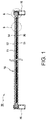
- FIG. 1 is a sectional view of the solar cell module 10 and FIG. 2 is an enlarged view of A portion in FIG. 1 .
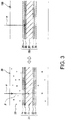
- FIG. 3 is an enlarged view of B portion in FIG. 1 and a structure of related art thereof is shown on the right side by way of comparison.
- each protective member, a conducting wire 14, and an electrode of a solar cell 11 are omitted.
- FIG. 4 is a sectional view of an encapsulant layer 30.
- the conducting wire 14 is also omitted in FIG. 4 .
- a wavelength conversion material 33 is denoted by " ⁇ " for the purpose of illustration.
- FIG. 5 is a diagram showing a modification example of the embodiment.
- the solar cell module 10 includes a plurality of solar cells 11, a first protective member 12 provided on a light-receiving-surface side of the solar cells 11, and a second protective member 13 provided on a rear-surface side of the solar cells 11.
- the solar cells 11 are sandwiched between the first protective member 12 and the second protective member 13 and are sealed by the encapsulant layer 30 provided between the respective protective members.
- at least a gap region 32x of a rear-surface side area 32 in the encapsulant layer 30, the gap region 32x corresponding to a gap between the solar cells 11, contains the wavelength conversion material 33 which absorbs the light of a specific wavelength and converts the light into a light of a longer wavelength.
- the wavelength conversion material 33 may be contained in only the gap region 32x, or may be contained in substantially the entire area of the rear-surface side area 32. In the latter case, a concentration of the wavelength conversion material 33 is set to be higher in the gap region 32x than in a region (hidden region 32y) sandwiched between the rear surface of the solar cell 11 and the second protective member 12. In the former case, since the concentration of the wavelength conversion material 33 in the hidden region 32y is 0%, the concentration of the wavelength conversion material 33 is obviously higher in the gap region 32x than in the hidden region 32y.
- the encapsulant layer 30 is also referred to as a filler layer (filler).
- the plurality of solar cells 11 are arranged substantially on the same plane.
- the solar cells 11 that are adjacent to each other are connected in series through the conducting wire 14, which forms a string of the solar cells 11.
- the conducting wire 14 is bent in a thickness direction of the module between the adjacent solar cells 11, and attached to each of the light receiving surface of one solar cell 11 and the rear surface of the other solar cell 11 by use of an adhesive or the like.
- a part of the conducting wire 14 is extended from an end of the string and connected with a wiring material for output (not shown).
- the wiring material is drawn out from, for example, a rear side of the second protective member 13 to be drawn into a terminal box (not shown).
- the solar cell 11, the first protective member 12, the second protective member 13, and the encapsulant layer 30 constitute a solar cell panel 15.
- the solar cell panel 15 is a plate-like body having the string of the solar cells 11 sandwiched between the respective protective members as described above, and has a substantially rectangular shape in a plane view (in a case viewed from a direction vertical to the light receiving surface), for example.
- the second protective member 13 may be bent around to, for example, a lateral face 15a of the solar cell panel 15 to cover the lateral face 15a.
- the lateral face 15a is a face along a thickness direction of the solar cell panel 15.
- the first protective member 12 may include a member having translucency such as a glass substrate, a resin substrate, or a resin film, for example.
- the glass substrate is preferably used from the viewpoint of fire resistance, durability or the like.
- a thickness of the glass substrate is not specifically limited, but is preferably about 2 mm to 6 mm.
- the second protective member 13 may include a transparent member the same as for the first protective member 12 and may include a non-transparent member.
- the embodiment uses the resin film as the second protective member 13.
- the resin film is not specifically limited, but is preferably a polyethylene terephthalate (PET) film. From the viewpoint of lowering moisture permeability or the like, the resin film may have formed therein an inorganic compound layer of silica and the like, or a metal layer of aluminium and the like in a case where it is not assumed that the light is incident on the rear-surface side.
- a thickness of the resin film is not specifically limited, but is preferably 100 ⁇ m to 300 ⁇ m.
- the solar cell module 10 preferably includes a frame 16 attached to an end edge of the solar cell panel 15.
- the frame 16 protects the end edge of the solar cell panel 15 and is used when the solar cell module 10 is installed on a roof or the like.
- the frame 16 is made of a metal such as stainless-steel, aluminium or the like, for example, and has a main body of a hollow construction and a concave portion in which the end edge of the solar cell panel 15 is fitted.
- the solar cell module 10 preferably includes a reflector 18 which is provided to cover the lateral face 15a of the solar cell panel 15.
- the reflector 18 reflects the light wavelength-converted by the wavelength conversion material 33 and confines the light to go out from the end edge of the solar cell panel 15 to the panel, functioning to increase the light incident on the solar cell 11.
- the reflector 18 reflects also light other than the wavelength-converted light. Since the wavelength conversion material 33 having absorbed the light of a specific wavelength isotropically emits the light, installation of the reflector 18 is particularly effective in the solar cell module 10 provided with the wavelength conversion material 33.
- the reflector 18 preferably covers substantially the entire lateral face 15a and covers a light receiving surface of the first protective member 12 and a rear surface of the second protective member 13 which are located at the end edge of the solar cell panel 15.
- the reflector 18 is preferably limited to be provided at a portion on each protective member covered by the frame 16.
- the reflector 18 which is, for example, a resin sheet containing a white pigment or the like is attached to the end edge of the solar cell panel 15.
- a coating film may be formed on the end edge of the solar cell panel 15 or the concave portion of the frame 16 by use of a white paint and the coating film used as the reflector 18.
- the adhesive 17 to which the white pigment or the like is added may be made to function as the reflector 18.
- the solar cell 11 includes a photoelectric conversion part 20 which receives sunlight to generate carriers.
- the photoelectric conversion part 20 has, as electrodes for collecting the generated carriers, a light-receiving-surface electrode formed on the light receiving surface of the photoelectric conversion part 20 and a rear-surface electrode formed on the rear surface (neither not shown). Each electrode is electrically connected with the conducting wire 14.
- a structure of the solar cell 11 is not limited thereto, and may have a structure in which the electrode is formed only on the rear surface of the photoelectric conversion part 20, for example.
- the rear-surface electrode is preferably formed to have an area larger than the light-receiving-surface electrode, and a surface having a larger electrode area (or a surface having the electrode formed thereon) may be said to be the "rear surface" of the solar cell 11.
- the photoelectric conversion part 20 has, for example, a semiconductor substrate 21, amorphous semiconductor layers 22 and 23 formed on the substrate, and transparent conductive layers 24 and 25 formed on the amorphous semiconductor layers.
- the semiconductor constituting the semiconductor substrate 21 include crystalline silicon (c-Si), gallium arsenide (GaAs), indium phosphide (InP) and the like.
- the amorphous semiconductor constituting the amorphous semiconductor layers 22 and 23 include i-type amorphous silicon, n-type amorphous silicon, p-type amorphous silicon and the like.
- the transparent conductive layers 24 and 25 preferably include a transparent conductive oxide in which metal oxide such as indium oxide (In 2 O 3 ), zinc oxide (ZnO) is doped with tin (Sn), antimony (Sb) or the like.
- an n-type single-crystal silicon substrate is applied to the semiconductor substrate 21.
- the photoelectric conversion part 20 has a structure in which an i-type amorphous silicon layer, a p-type amorphous silicon layer, and the transparent conductive layer 24 are formed in this order on a light receiving surface of the n-type single-crystal silicon substrate, and an i-type amorphous silicon layer, an n-type amorphous silicon layer, and the transparent conductive layer 25 are formed in this order on a rear surface of the substrate.
- the p-type amorphous silicon layer may be formed on the rear-surface side of the n-type single-crystal silicon substrate and the n-type amorphous silicon layer may be formed on the light-receiving-surface side of the substrate, respectively.
- the photoelectric conversion part 20 has a junction (heterojunction) between the semiconductors in which optical gaps are different from each other.
- the amorphous silicon layer forming the heterojunction generally absorbs the light having a wavelength of 600 nm or less.
- the wavelength conversion material 33 contained in the encapsulant layer 30 preferably absorbs and wavelength-converts the light of a wavelength having an energy equal to or more than a bandgap of the amorphous semiconductor layers 22 and 23, which are each a heterojunction layer.
- the encapsulant layer 30 which is provided between each protective member and the solar cell 11 functions to prevent moisture or the like from contacting the solar cell 11.
- the encapsulant layer 30 contains the wavelength conversion material 33 in at least the gap region 32x of the rear-surface side area 32.
- the wavelength conversion material 33 is also contained in the light-receiving-surface side area 31 and the hidden region 32y of the rear-surface side area 32.
- the wavelength conversion material 33 is preferably contained in the end edge of the solar cell panel 15, that is, is between the lateral face 15a of the solar cell panel 15 and the solar cell 11 positioned at an end of the string.
- the light-receiving-surface side area 31 is an area in the encapsulant layer 30 located closer to the first protective member 12 side than the solar cell 11.
- the rear-surface side area 32 is an area in the encapsulant layer 30 located closer to the second protective member 13 side than the solar cell 11.
- the gap region 32x is an area corresponding to a gap between the solar cells 11 in the rear-surface side area 32.
- the hidden region 32y is an area sandwiched between the rear surface of the solar cell 11 and the second protective member 13 in the rear-surface side area 32.
- the encapsulant layer 30 is preferably formed in a laminating process described later using a resin sheet constituting the light-receiving-surface side area 31 (hereinafter, referred to as "resin sheet 31”) and a resin sheet constituting the rear-surface side area 32 (hereinafter, referred to as "resin sheet 32").
- resin sheet 31 a resin sheet constituting the light-receiving-surface side area
- resin sheet 32 a resin sheet constituting the rear-surface side area 32
- FIG. 4 a boundary between the light-receiving-surface side area 31 and the rear-surface side area 32 is clearly defined, but the boundary may not be confirmed in some cases, depending on a kind of the resin and conditions of the laminating process.
- the resin constituting the encapsulant layer 30 is preferably one having excellent adhesion to each protective member and the solar cell 11, and unlikely to be permeable to moisture.
- the resins include an olefin-based resin obtained by polymerizing at least one kind selected from ⁇ olefin having the carbon number of 2 to 20 (e.g., polyethylene, polypropylene, a random or block copolymer of ethylene and other ⁇ olefin, etc.), an ester-based resin (e.g., polycondensate of polyol and polycarboxylic acid or acid anhydride/lower alkyl ester, etc.), a urethane-based resin (e.g., polyaddition compound of polyisocyanate and active hydrogen group-containing compound (diol, polyol riol, dicarboxylic acid, polycarboxylic acid, polyamine, polythiol, etc.) or the like), an epoxy-based resin (e.g., ring-
- olefin-based resin in particular, polymer including ethylene
- olefin-based resin in particular, polymer including ethylene
- Ethylene vinyl acetate copolymer EVA is particularly preferable as the copolymer of ⁇ olefin and carboxylic acid vinyl.
- the thickness of the encapsulant layer 30 is not specifically limited, but the thicknesses of the light-receiving-surface side area 31 and the rear-surface side area 32 are each preferably about 100 to 600 ⁇ m.
- a high crosslink density resin is generally preferably used for the light-receiving-surface side area 31 and a low crosslink density resin or non-crosslinked resin is generally preferably used for the rear-surface side area 32, depending on the structure or intended purpose (usage environment) of the solar cell module 10.
- a refractive index of the encapsulant layer 30 is preferably set to be higher than a refractive index of an outermost layer of the first protective member 12 at the area containing the wavelength conversion material 33.
- the refractive index of the encapsulant layer 30 is preferably set to be higher than the refractive index of a glass surface.
- the refractive index of the encapsulant layer 30 can be adjusted by, for example, adequately changing a composition of resin components.
- the wavelength conversion material 33 having absorbed the light of a specific wavelength isotropically emits the light, there exists light passing through the glass to go out from the panel, but a totally reflected component at the glass surface is increased by the adjustment of the refractive index, preventing the relevant light from going out.
- the wavelength conversion material 33 which is a material absorbing light of a specific wavelength and converting the wavelength as described above, converts light in a wavelength region contributing less to power generation into light in a wavelength region contributing largely to power generation.
- the wavelength conversion material 33 absorbs ultraviolet rays that are light of a shorter wavelength than 380 nm, for example, to convert into light of a longer wavelength (e.g., 400 to 800 nm). In this case, the wavelength conversion material 33 also contributes to deterioration suppression of the constituent material due to the ultraviolet rays.
- the wavelength conversion material 33 is preferably one that absorbs the ultraviolet rays to emit visible light, but may be a material that absorbs visible light or infrared light. In general, the wavelength conversion material 33 converts the shorter wavelength into the longer wavelength, but may be a material performing a so-called upconversion emission in which the longer wavelength is converted into the shorter wavelength. A preferable converted wavelength depends on a kind of the solar cell 11.
- the wavelength conversion material 33 preferably absorbs and wavelength-converts the light of a wavelength having an energy equal to or more than a bandgap of the heterojunction layer, as described above. In other words, the wavelength conversion material 33 preferably converts the light of the wavelength absorbed into the heterojunction layer.
- the wavelength conversion material 33 is preferably used which can absorb light ⁇ of a wavelength ⁇ absorbed by the amorphous semiconductor layers 22 and 23 which are each the heterojunction layer to convert into light ⁇ of a wavelength ⁇ not absorbed by the semiconductor layers (see FIG. 3 ).
- ⁇ is equal to or less than 600 nm, for example.
- a part of the light ⁇ is absorbed by the amorphous semiconductor layers 22 and 23.
- the wavelength conversion material 33 examples include semiconductor nanoparticles (quantum dot), luminescent metal complexes, organic fluorescent dyes and the like.
- semiconductor nanoparticle examples include nanoparticles of zinc oxide (ZnO), cadmium selenide (CdSe), cadmium telluride (CdTe), gallium nitride (GaN), yttrium oxide (Y 2 O 3 ), indium phosphide (InP) and the like.
- the luminescent metal complex examples include an Ir complex such as [Ir(bqn) 3 ](PF 6 ) 3 , [Ir(dpbpy) 3 ](PF 6 ) 3 or the like, a Ru complex such as [Ru(bqn) 3 ](PF 6 ) 3 , [Ru(bpy) 3 ](ClO 4 ) 2 or the like, an Eu complex such as [Eu(FOD) 3 ]phen, [Eu(TFA) 3 ]phen or the like, and a Tb complex such as [Tb(FOD) 3 ]phen, [Tb(HFA) 3 ]phen or the like.
- the organic fluorescent dye examples include a rhodamine-based dye, a coumarin-based dye, a fluorescein-based dye, a perylene-based dye and the like.
- ⁇ 33 a concentration of the wavelength conversion material 33 in the respective areas of the encapsulant layer 30.
- the gap region 32x and the hidden region 32y are different from each other with respect to ⁇ 33 in the rear-surface side area 32 (see FIG. 4 ). This allows the usage efficiency of the wavelength conversion material 33 to be improved, for example.
- ⁇ 33 is set to be higher in the gap region 32x than in the hidden region 32y. In other words, it is preferable that a concentration gradient of the wavelength conversion material 33 exists in the rear-surface side area 32 and the wavelength conversion material 33 is biasedly held in the gap region 32x.
- ⁇ 33 in the end edge of the solar cell panel 15 may be, for example, substantially the same as ⁇ 33 in the gap region 32x.
- ⁇ 33 in the gap region 32x> ⁇ 33 in the hidden region 32y should hold is due to a difference in an amount of incident light in the gap region 32x and in the hidden region 32y.
- the hidden region 32y is a region hidden by the solar cell 11 when seen from the light-receiving-surface side as well as a region with a lower amount of incident light.
- the gap region 32x is a region with a larger amount of incident light because the solar cell 11 does not exist on the light-receiving-surface side. Therefore, the wavelength conversion material 33 being biasedly held in the gap region 32x is important in efficiently using the wavelength conversion material 33, which is expensive. This allows the wavelength conversion efficiency to be enhanced while suppressing a usage amount of the wavelength conversion material 33.
- the wavelength conversion material 33 is preferably biasedly held in the gap region 32x.
- the wavelength conversion material 33 is preferably used which is capable of conversion into a light of a wavelength close to reflected light from the solar cell 11.
- a wavelength conversion material 33 which absorbs the ultraviolet rays having a wavelength of 380 nm or less to convert into light having a wavelength close to the blue color (e.g., 450 to 490 nm).
- the concentration gradient of the wavelength conversion material 33 may exist in a thickness direction of the rear-surface side area 32.
- the wavelength conversion material 33 may be contained in, for example, an area adjacent to the solar cell 11 (light-receiving-surface side area 31) in larger amounts than in an area adjacent to the second protective member 13, and the closer to the second protective member 13, the more ⁇ 33 may be decreased gradually or in a stepwise fashion.
- ⁇ 33 in the gap region 32x is preferably 0.1 to 15 wt% with respect to a total weight of the gap region 32x and more preferably 1.5 to 10 wt%, in a case where the wavelength conversion material 33 is an inorganic system compound such as a semiconductor nanoparticle, a luminescent metal complex and the like.
- ⁇ 33 is preferably 0.02 to 2.0 wt% with respect to the total weight of the gap region 32x and more preferably 0.05 to 0.8 wt%, in a case where the wavelength conversion material 33 is an organic system compound such as an organic fluorescent dye and the like.
- ⁇ 33 in the hidden region 32y is preferably 0 to 5 wt% with respect to a total weight of the hidden region 32y and more preferably 0 to 2 wt%, in a case where the wavelength conversion material 33 is an inorganic system compound.
- ⁇ 33 is preferably is 0 to 0.5 wt% with respect to the total weight of the hidden region 32y and more preferably 0 to 0.1 wt%, in a case where the wavelength conversion material 33 is an organic system compound.
- ⁇ 33 in the light-receiving-surface side area 31 is substantially uniform, for example.
- the wavelength conversion material 33 may be contained in an area adjacent to the first protective member 12 in larger amounts than in an area adjacent to solar cell 11, and the closer to the second protective member 13, the more ⁇ 33 may be decreased gradually or in a stepwise fashion.
- ⁇ 33 in the light-receiving-surface side area 31 and ⁇ 33 in the gap region 32x may be substantially the same as or different from each other. From the viewpoint of incident photon-to-current conversion efficiency improvement, ⁇ 33 in the light-receiving-surface side area 31 ⁇ 33 in the gap region 32x preferably holds. In order to reduce the above contrast to make the look refined, ⁇ 33 in the light-receiving-surface side area 31 ⁇ 33 gap region 32x may hold. In either case, both ⁇ 33 in the light-receiving-surface side area 31 and ⁇ 33 in the gap region 32x> ⁇ 33 in the hidden region 32y preferably holds.
- an ultraviolet-ray absorption material, an antioxidizing agent, a flame retardant or the like, besides the wavelength conversion material 33, may be added to the encapsulant layer 30.
- a pigment of titanium oxide or the like may be added to the rear-surface side area 32 in a case where it is not assumed that the light is incident on the rear-surface side.
- the ultraviolet-ray absorption material which is a material selectively absorbing ultraviolet rays that are light of a shorter wavelength than 380 nm, does not have a wavelength-conversion function like the wavelength conversion material 33.
- ultraviolet-ray absorption material examples include a benzotriazole-based compound, a benzophenone-based compound, a salicylate-based compound, a cyanoacrylate-based compound, a nickel-based compound, a triazine-based compound, and the like.
- the solar cell module 10 including the above structure can be manufactured by laminating the string of the solar cells 11 connected by the conducting wire 14, by use of the resin sheet constituting the first protective member 12, the second protective member 13, and the encapsulant layer 30.
- the first protective member 12, the resin sheet 31, the string of the solar cells 11, the resin sheet 32, and the second protective member 13 are laminated in this order on a heater, for example.
- This laminated body is heated to about 150°C in a vacuum state. After that, heating is continued under an atmospheric pressure with each constituent member being pressed to the heater side to crosslink resin components in the resin sheet, obtaining the solar cell panel 15.
- the reflector 18, the terminal box, the frame 16 and the like are attached to the solar cell panel 15 to obtain the solar cell module 10.
- the concentration gradient of the wavelength conversion material 33 in the rear-surface side area 32 can be formed by using a plurality of resin sheets as the resin sheet 32 in which contents of the wavelength conversion material 33 are different from each other, for example.
- a resin sheet (referred to as resin sheet X) containing the wavelength conversion material 33 in large amounts, and a resin sheet (referred to as resin sheet Y) having a lower content of the wavelength conversion material 33 than the resin sheet X or not containing the wavelength conversion material 33 are used.
- the resin sheet X is arranged in a portion corresponding to the gap region 32x and the resin sheet Y is arranged in a portion corresponding to the hidden region 32y.
- a method may be used in which diffusion of the wavelength conversion material 33 from the light-receiving-surface side area 31 is used.
- the resin sheet 31 containing the wavelength conversion material 33, and the resin sheet 32 having lower content of the wavelength conversion material 33 than the resin sheet 31 or not containing the wavelength conversion material 33 are used. By laminating these, the wavelength conversion material 33 is diffused from the resin sheet 31 to a portion which is to be the gap region 32x in the resin sheet 32, obtaining the above concentration gradient of the wavelength conversion material 33 in the rear-surface side area 32.
- the usage efficiency of the incident light can be refined to improve the incident photon-to-current conversion efficiency.
- efficient use of the wavelength conversion material 33 is allowed by devising the concentration distributions of the wavelength conversion material 33 particularly in the rear-surface side area 32 of the encapsulant layer 30.
- the incident light can be used more efficiently by biasedly holding the wavelength conversion material 33 in the gap region 32x of the rear-surface side area 32, compared with the case where the wavelength conversion material 33 is not contained in the rear-surface side area 32 and the case where the wavelength conversion material 33 is uniformly contained in the rear-surface side area 32.
- the wavelength conversion material 33 which emits light of a wavelength close to a reflected light from the solar cell 11 can reduce the coloristic contrast between the region where the solar cell 11 exists and the region positioned at a gap between the solar cells. This allows a product that looks good and has excellent design to be obtained.
- the structure may be used in which the wavelength conversion material 33 is contained in only the gap region 36x.
- the wavelength conversion material 33 is substantially not contained in the light-receiving-surface side area 35 nor the hidden region 36y of the rear-surface side area 36.
- the concentration of the wavelength conversion material 33 is substantially 0% in the hidden region 36y.
- the wavelength conversion material 33 is preferably contained between the solar cell 11 positioned at the end of the string and the lateral face 15a of the solar cell panel 15 at the concentration substantially the same as the gap region 36x.
- the structure is particularly directed to the purpose of improving the design by reducing the contrast.
- FIG. 6 is a sectional view of an encapsulant layer 50 similar to FIG. 4 .
- FIG. 7 is a diagram showing a relationship between a transmittance and a wavelength of light in the encapsulant layer 50.
- FIG. 7 shows on the right a case of an encapsulant layer which contains only each of a first wavelength conversion material 33a and a second wavelength conversion material 33b by way of comparison.
- a different point from the first embodiment is mainly explained, and the same components as the first embodiment are designated by the same reference signs and duplicated description is omitted.
- a structure of the encapsulant layer 50 is different from the encapsulant layer 30 in the first embodiment.
- the encapsulant layer 50 is different from the encapsulant layer 30, which contains only one kind of wavelength conversion material 33, in that it contains two kinds, namely the first wavelength conversion material 33a and the second wavelength conversion material 33b.
- the second wavelength conversion material 33b is a material which absorbs and wavelength-converts light of a longer wavelength than the first wavelength conversion material 33a.
- the first wavelength conversion material 33a and the second wavelength conversion material 33b preferably have at least the maximal absorption wavelength not overlapping each other. Moreover, at least the maximum emission wavelength of the first wavelength conversion material 33a and the maximal absorption wavelength of the second wavelength conversion material 33b preferably do not overlap each other. Of course, it is particularly preferable that the first wavelength conversion material 33a substantially does not absorb the ultraviolet rays or the like absorbed by the second wavelength conversion material 33b, and the second wavelength conversion material 33b substantially does not absorb the light wavelength-converted by the first wavelength conversion material 33a.
- the first wavelength conversion material 33a and the second wavelength conversion material 33b are not specifically limited in individual materials so long as a combination thereof satisfies the above relationship, and the same material as the wavelength conversion material 33 may be used, for example.
- a perylene-based dye may be used for the first wavelength conversion material 33a and a fluorescein-based dye may be used for the second wavelength conversion material 33b.
- materials may be applied which are of the same kind as each other (e.g., perylene-based dye) and different from each other in wavelength conversion characteristics (absorption wavelength and emission wavelength).
- the first wavelength conversion material 33a is contained in a light-receiving-surface side area 51
- the second wavelength conversion material 33b is contained in a rear-surface side area 52.
- a concentration of the second wavelength conversion material 33b in the rear-surface side area 52 is higher in a gap region 52x than in a hidden region 52y.
- a part of the first wavelength conversion material 33a may be contained in the rear-surface side area 52, or a part of the second wavelength conversion material 33b may be contained in the light-receiving-surface side area 51.
- the first wavelength conversion material 33a is preferably contained in the gap region 52x in larger amounts than in the hidden region 52y.
- the first wavelength conversion material 33a and the second wavelength conversion material 33b are used to improve a conversion efficiency of the ultraviolet rays which contribute less to power generation and deteriorate the constituent material, for example.
- the ultraviolet rays close to the visible region for example, cannot be sufficiently converted in some cases.
- a part of the ultraviolet rays of a shorter wavelength for example, is difficult to convert.
- a concentration of the first wavelength conversion material 33a (hereinafter, referred to as " ⁇ 33a ”) is preferably higher in the light-receiving-surface side area 51 than the concentration of the second wavelength conversion material 33b.
- the concentration of the second wavelength conversion material 33b (hereinafter, referred to as “( ⁇ 33b ") is preferably higher in the rear-surface side area 52 than the concentration of the first wavelength conversion material 33a.
- the second wavelength conversion material 33b converting the light of a longer wavelength is likely to suffer damage from the light of a shorter wavelength compared to the first wavelength conversion material 33a, but deterioration of the second wavelength conversion material 33b can be suppressed by applying the relevant concentration distribution.
- the first wavelength conversion material 33a converts the light of a shorter wavelength which deteriorates the second wavelength conversion material 33b, protecting the second wavelength conversion material 33b.
- the light of a longer wavelength which the first wavelength conversion material 33a cannot convert may be converted by the second wavelength conversion material 33b contained in the rear-surface side area 52 in large amounts.
- ⁇ 33a in the light-receiving-surface side area 51 is preferably 0.1 to 15 wt% with respect to a total weight of the light-receiving-surface side area 51 and more preferably 1.5 to 10 wt%, in a case where the first wavelength conversion material 33a is an inorganic system compound.
- ⁇ 33a is preferably 0.02 to 2.0 wt% with respect to the total weight of the light-receiving-surface side area 51 and more preferably 0.05 to 0.8 wt%, in a case where the first wavelength conversion material 33a is an organic system compound.
- ⁇ 33b in the light-receiving-surface side area 51 is preferably 0 to 1.5 wt% with respect to the total weight of the rear-surface side area 51 and more preferably 0 to 0.1 wt% in a case where the second wavelength conversion material 33b is an inorganic system compound.
- ⁇ 33b is preferably 0 to 0.05 wt% with respect to the total weight of the rear-surface side area 51 and more preferably 0 to 0.02 wt% in a case where the second wavelength conversion material 33b is an organic system compound.
- ⁇ 33a in the rear-surface side area 52 is preferably 0 to 1.5 wt% with respect to a total weight of the rear-surface side area 52 and more preferably 0 to 0.1 wt% in a case where the first wavelength conversion material 33a is an inorganic system compound.
- ⁇ 33a is preferably 0 to 0.05 wt% with respect to the total weight of the rear-surface side area 52 and more preferably 0 to 0.02 wt% in a case where the first wavelength conversion material 33a is an organic system compound.
- ⁇ 33b in gap region 52x of the rear-surface side area 52 is preferably 0.1 to 15 wt% with respect to a total weight of the gap region 52x and more preferably 1.5 to 10 wt%, in a case where the second wavelength conversion material 33b is an inorganic system compound.
- ⁇ 33b is preferably 0.02 to 2.0 wt% with respect to the total weight of the gap region 52x and more preferably 0.05 to 0.8 wt%, in a case where the second wavelength conversion material 33b is an organic system compound.
- ⁇ 33a is set to be lower than ⁇ 33b in the light-receiving-surface side area 51 and ⁇ 33a is set to be higher than ⁇ 33b in the rear-surface side area 52 to suppress duplicated wavelength conversion, enhancing the wavelength conversion efficiency.
- the case is shown where two kinds of wavelength conversion material, namely the first wavelength conversion material 33a and the second wavelength conversion material 33b, are used, but three or more kinds of wavelength conversion materials may be used.
Landscapes
- Photovoltaic Devices (AREA)
Applications Claiming Priority (2)
| Application Number | Priority Date | Filing Date | Title |
|---|---|---|---|
| JP2014035110 | 2014-02-26 | ||
| PCT/JP2015/000632 WO2015129183A1 (ja) | 2014-02-26 | 2015-02-12 | 太陽電池モジュール |
Publications (2)
| Publication Number | Publication Date |
|---|---|
| EP3113233A1 true EP3113233A1 (de) | 2017-01-04 |
| EP3113233A4 EP3113233A4 (de) | 2017-03-08 |
Family
ID=54008521
Family Applications (1)
| Application Number | Title | Priority Date | Filing Date |
|---|---|---|---|
| EP15754831.4A Withdrawn EP3113233A4 (de) | 2014-02-26 | 2015-02-12 | Solarzellenmodul |
Country Status (4)
| Country | Link |
|---|---|
| US (1) | US10930807B2 (de) |
| EP (1) | EP3113233A4 (de) |
| JP (1) | JP6583828B2 (de) |
| WO (1) | WO2015129183A1 (de) |
Families Citing this family (5)
| Publication number | Priority date | Publication date | Assignee | Title |
|---|---|---|---|---|
| CN110998866B (zh) * | 2017-08-10 | 2022-12-06 | 株式会社钟化 | 太阳能电池模块 |
| CN108123671A (zh) * | 2017-11-29 | 2018-06-05 | 北京创昱科技有限公司 | 一种框架压缩装置及薄膜拉伸方法 |
| US11695089B2 (en) | 2019-12-31 | 2023-07-04 | Industrial Technology Research Institute | Solar cell modules |
| EP3846227B1 (de) * | 2019-12-31 | 2022-05-04 | Industrial Technology Research Institute | Solarzellenmodule |
| WO2022083370A1 (zh) * | 2021-09-16 | 2022-04-28 | 星昱科技(上海)有限公司 | 发光太阳能收集装置及其制作方法 |
Family Cites Families (19)
| Publication number | Priority date | Publication date | Assignee | Title |
|---|---|---|---|---|
| US20040131792A1 (en) * | 2001-03-22 | 2004-07-08 | Bhattacharya Raghu N. | Electroless deposition of cu-in-ga-se film |
| JP2008311604A (ja) * | 2007-02-06 | 2008-12-25 | Hitachi Chem Co Ltd | 太陽電池モジュール及び太陽電池モジュール用波長変換型集光フィルム |
| WO2008110567A1 (en) * | 2007-03-13 | 2008-09-18 | Basf Se | Photovoltaic modules with improved quantum efficiency |
| EP2203943A4 (de) * | 2007-10-12 | 2015-10-14 | Omnipv Inc | Solarmodule mit vergrösserten wirkungsgraden durch verwendung von spektralen konzentratoren |
| JP2010034489A (ja) * | 2008-06-30 | 2010-02-12 | Mitsubishi Chemicals Corp | 膜状太陽電池及び太陽電池パネル |
| JP2011238639A (ja) * | 2010-05-06 | 2011-11-24 | Toppan Printing Co Ltd | 太陽電池モジュール用封止材シート及び太陽電池モジュール |
| EP2579329A1 (de) | 2010-05-26 | 2013-04-10 | Hitachi Chemical Company, Ltd. | Dichtmaterial für solarzellen mit wellenlängenumwandlung und solarzellenmodul |
| JP2012069865A (ja) * | 2010-09-27 | 2012-04-05 | Toppan Printing Co Ltd | 太陽電池封止材及びそれを用いた太陽電池モジュール |
| US9525092B2 (en) * | 2010-11-05 | 2016-12-20 | Pacific Light Technologies Corp. | Solar module employing quantum luminescent lateral transfer concentrator |
| CN103477446A (zh) * | 2011-03-31 | 2013-12-25 | 陶氏环球技术有限公司 | 包含下转换材料的透光热塑性树脂及其在光伏模块中的用途 |
| JP2012216620A (ja) * | 2011-03-31 | 2012-11-08 | Denso Corp | 太陽電池モジュール |
| JP2012230968A (ja) * | 2011-04-25 | 2012-11-22 | Hitachi Chem Co Ltd | 封止材シート及び太陽電池モジュール |
| JP2013065595A (ja) * | 2011-09-15 | 2013-04-11 | Hitachi Chemical Co Ltd | 波長変換型太陽電池封止材、及び太陽電池モジュール |
| US9399730B2 (en) * | 2011-12-06 | 2016-07-26 | Nitto Denko Corporation | Wavelength conversion material as encapsulate for solar module systems to enhance solar harvesting efficiency |
| JP2013120926A (ja) * | 2011-12-06 | 2013-06-17 | Nitto Denko Corp | 太陽光集光効率を高めるためのソーラーモジュールシステムの封止材としての波長変換物質 |
| FR2988222B1 (fr) * | 2012-03-13 | 2016-06-24 | Commissariat Energie Atomique | Module photovoltaique comprenant des elements de conversion spectrale localises et procede de realisation |
| JP2013254854A (ja) * | 2012-06-07 | 2013-12-19 | Sharp Corp | 太陽電池モジュールおよび太陽光発電装置 |
| KR20150135346A (ko) * | 2013-03-26 | 2015-12-02 | 닛토덴코 가부시키가이샤 | 다중 광안정성 유기 발색단을 갖는 파장 변환 필름 |
| JP2013128153A (ja) * | 2013-03-27 | 2013-06-27 | Hitachi Ltd | 封止材シートおよび太陽電池モジュール |
-
2015
- 2015-02-12 JP JP2016505028A patent/JP6583828B2/ja not_active Expired - Fee Related
- 2015-02-12 EP EP15754831.4A patent/EP3113233A4/de not_active Withdrawn
- 2015-02-12 WO PCT/JP2015/000632 patent/WO2015129183A1/ja not_active Ceased
-
2016
- 2016-08-17 US US15/239,327 patent/US10930807B2/en not_active Expired - Fee Related
Also Published As
| Publication number | Publication date |
|---|---|
| JPWO2015129183A1 (ja) | 2017-03-30 |
| WO2015129183A1 (ja) | 2015-09-03 |
| JP6583828B2 (ja) | 2019-10-02 |
| EP3113233A4 (de) | 2017-03-08 |
| US20160359064A1 (en) | 2016-12-08 |
| US10930807B2 (en) | 2021-02-23 |
Similar Documents
| Publication | Publication Date | Title |
|---|---|---|
| US20160336470A1 (en) | Solar cell module | |
| US20170288080A1 (en) | Luminescent Electricity-Generating Window for Plant Growth | |
| US10930807B2 (en) | Solar cell module | |
| EP2648229A1 (de) | Solarzellenmodul und herstellungsverfahren dafür | |
| US20190273171A1 (en) | Solar window | |
| US20170018672A1 (en) | High power solar cell module | |
| WO2016146676A1 (en) | Solal panel photo-luminescent layer | |
| US20190148578A1 (en) | Solar cell module | |
| KR102770504B1 (ko) | 미디어 건물 일체형 태양광 모듈 | |
| KR102521335B1 (ko) | 광합성 파장 투과형 발광태양광 패널 및 그 제조방법 | |
| US20130037084A1 (en) | Photovoltaic Module Light Manipulation for Increased Module Output | |
| KR20140012226A (ko) | 태양전지 모듈 | |
| KR20220166520A (ko) | 태양광 모듈 및 이의 제조 방법 | |
| KR102514859B1 (ko) | 미디어 건물 일체형 태양광 모듈 | |
| JP6655798B2 (ja) | 太陽電池モジュールの製造方法 | |
| KR102532077B1 (ko) | 미디어 건물 일체형 태양광 모듈 및 이를 이용한 영상 구현시스템 | |
| WO2017207558A1 (en) | Distributed photovoltaic cell panel | |
| WO2015190047A1 (ja) | 太陽電池モジュール | |
| JP2017188525A (ja) | 太陽電池モジュール及び太陽光発電システム | |
| JPWO2015145925A1 (ja) | 太陽電池モジュール |
Legal Events
| Date | Code | Title | Description |
|---|---|---|---|
| PUAI | Public reference made under article 153(3) epc to a published international application that has entered the european phase |
Free format text: ORIGINAL CODE: 0009012 |
|
| STAA | Information on the status of an ep patent application or granted ep patent |
Free format text: STATUS: REQUEST FOR EXAMINATION WAS MADE |
|
| 17P | Request for examination filed |
Effective date: 20160923 |
|
| AK | Designated contracting states |
Kind code of ref document: A1 Designated state(s): AL AT BE BG CH CY CZ DE DK EE ES FI FR GB GR HR HU IE IS IT LI LT LU LV MC MK MT NL NO PL PT RO RS SE SI SK SM TR |
|
| AX | Request for extension of the european patent |
Extension state: BA ME |
|
| A4 | Supplementary search report drawn up and despatched |
Effective date: 20170208 |
|
| RIC1 | Information provided on ipc code assigned before grant |
Ipc: H01L 31/055 20140101AFI20170202BHEP Ipc: H01L 31/048 20140101ALI20170202BHEP Ipc: H02S 30/10 20140101ALI20170202BHEP Ipc: H01L 31/054 20140101ALI20170202BHEP |
|
| DAX | Request for extension of the european patent (deleted) | ||
| RAP1 | Party data changed (applicant data changed or rights of an application transferred) |
Owner name: PANASONIC INTELLECTUAL PROPERTY MANAGEMENT CO., LT |
|
| STAA | Information on the status of an ep patent application or granted ep patent |
Free format text: STATUS: EXAMINATION IS IN PROGRESS |
|
| 17Q | First examination report despatched |
Effective date: 20200528 |
|
| GRAP | Despatch of communication of intention to grant a patent |
Free format text: ORIGINAL CODE: EPIDOSNIGR1 |
|
| STAA | Information on the status of an ep patent application or granted ep patent |
Free format text: STATUS: GRANT OF PATENT IS INTENDED |
|
| INTG | Intention to grant announced |
Effective date: 20220214 |
|
| STAA | Information on the status of an ep patent application or granted ep patent |
Free format text: STATUS: THE APPLICATION IS DEEMED TO BE WITHDRAWN |
|
| 18D | Application deemed to be withdrawn |
Effective date: 20220625 |