EP3113235A1 - Elektrolumineszenzvorrichtung - Google Patents
Elektrolumineszenzvorrichtung Download PDFInfo
- Publication number
- EP3113235A1 EP3113235A1 EP16176191.1A EP16176191A EP3113235A1 EP 3113235 A1 EP3113235 A1 EP 3113235A1 EP 16176191 A EP16176191 A EP 16176191A EP 3113235 A1 EP3113235 A1 EP 3113235A1
- Authority
- EP
- European Patent Office
- Prior art keywords
- layer
- filling material
- alloy
- metal layer
- type
- Prior art date
- Legal status (The legal status is an assumption and is not a legal conclusion. Google has not performed a legal analysis and makes no representation as to the accuracy of the status listed.)
- Granted
Links
Images


Classifications
-
- H—ELECTRICITY
- H10—SEMICONDUCTOR DEVICES; ELECTRIC SOLID-STATE DEVICES NOT OTHERWISE PROVIDED FOR
- H10H—INORGANIC LIGHT-EMITTING SEMICONDUCTOR DEVICES HAVING POTENTIAL BARRIERS
- H10H20/00—Individual inorganic light-emitting semiconductor devices having potential barriers, e.g. light-emitting diodes [LED]
- H10H20/80—Constructional details
- H10H20/81—Bodies
- H10H20/822—Materials of the light-emitting regions
- H10H20/824—Materials of the light-emitting regions comprising only Group III-V materials, e.g. GaP
- H10H20/825—Materials of the light-emitting regions comprising only Group III-V materials, e.g. GaP containing nitrogen, e.g. GaN
- H10H20/8252—Materials of the light-emitting regions comprising only Group III-V materials, e.g. GaP containing nitrogen, e.g. GaN characterised by the dopants
-
- H—ELECTRICITY
- H10—SEMICONDUCTOR DEVICES; ELECTRIC SOLID-STATE DEVICES NOT OTHERWISE PROVIDED FOR
- H10H—INORGANIC LIGHT-EMITTING SEMICONDUCTOR DEVICES HAVING POTENTIAL BARRIERS
- H10H20/00—Individual inorganic light-emitting semiconductor devices having potential barriers, e.g. light-emitting diodes [LED]
- H10H20/80—Constructional details
- H10H20/81—Bodies
- H10H20/817—Bodies characterised by the crystal structures or orientations, e.g. polycrystalline, amorphous or porous
- H10H20/818—Bodies characterised by the crystal structures or orientations, e.g. polycrystalline, amorphous or porous within the light-emitting regions
-
- H—ELECTRICITY
- H10—SEMICONDUCTOR DEVICES; ELECTRIC SOLID-STATE DEVICES NOT OTHERWISE PROVIDED FOR
- H10H—INORGANIC LIGHT-EMITTING SEMICONDUCTOR DEVICES HAVING POTENTIAL BARRIERS
- H10H20/00—Individual inorganic light-emitting semiconductor devices having potential barriers, e.g. light-emitting diodes [LED]
- H10H20/80—Constructional details
- H10H20/81—Bodies
- H10H20/819—Bodies characterised by their shape, e.g. curved or truncated substrates
-
- H—ELECTRICITY
- H10—SEMICONDUCTOR DEVICES; ELECTRIC SOLID-STATE DEVICES NOT OTHERWISE PROVIDED FOR
- H10H—INORGANIC LIGHT-EMITTING SEMICONDUCTOR DEVICES HAVING POTENTIAL BARRIERS
- H10H20/00—Individual inorganic light-emitting semiconductor devices having potential barriers, e.g. light-emitting diodes [LED]
- H10H20/80—Constructional details
- H10H20/81—Bodies
- H10H20/819—Bodies characterised by their shape, e.g. curved or truncated substrates
- H10H20/82—Roughened surfaces, e.g. at the interface between epitaxial layers
-
- H—ELECTRICITY
- H10—SEMICONDUCTOR DEVICES; ELECTRIC SOLID-STATE DEVICES NOT OTHERWISE PROVIDED FOR
- H10H—INORGANIC LIGHT-EMITTING SEMICONDUCTOR DEVICES HAVING POTENTIAL BARRIERS
- H10H20/00—Individual inorganic light-emitting semiconductor devices having potential barriers, e.g. light-emitting diodes [LED]
- H10H20/80—Constructional details
- H10H20/81—Bodies
- H10H20/819—Bodies characterised by their shape, e.g. curved or truncated substrates
- H10H20/821—Bodies characterised by their shape, e.g. curved or truncated substrates of the light-emitting regions, e.g. non-planar junctions
-
- H—ELECTRICITY
- H10—SEMICONDUCTOR DEVICES; ELECTRIC SOLID-STATE DEVICES NOT OTHERWISE PROVIDED FOR
- H10H—INORGANIC LIGHT-EMITTING SEMICONDUCTOR DEVICES HAVING POTENTIAL BARRIERS
- H10H20/00—Individual inorganic light-emitting semiconductor devices having potential barriers, e.g. light-emitting diodes [LED]
- H10H20/80—Constructional details
- H10H20/83—Electrodes
- H10H20/831—Electrodes characterised by their shape
-
- H—ELECTRICITY
- H10—SEMICONDUCTOR DEVICES; ELECTRIC SOLID-STATE DEVICES NOT OTHERWISE PROVIDED FOR
- H10H—INORGANIC LIGHT-EMITTING SEMICONDUCTOR DEVICES HAVING POTENTIAL BARRIERS
- H10H20/00—Individual inorganic light-emitting semiconductor devices having potential barriers, e.g. light-emitting diodes [LED]
- H10H20/80—Constructional details
- H10H20/83—Electrodes
- H10H20/832—Electrodes characterised by their material
- H10H20/833—Transparent materials
Definitions
- the present invention relates to an electroluminescent device for emitting radiation in a spectral range.
- such a device of the state of the art is obtained by successive epitaxies of the second layer, the electroluminescent layer, and the first layer on a growth substrate, sapphire or AlGaN. Then, the metal layer is formed on the epitaxial layers. The assembly is then transferred to a host substrate, a good heat conductor. Finally, the growth substrate is removed by laser lift-off (" Laser Lift-off" in English). The texturing of the outer surface of the second layer is obtained by a selective chemical attack, based on KOH.
- the III / N type alloys have a hexagonal wurtzite crystal structure, and the defects take the form of cavities, emerging at the dislocations, especially at the first surface of the first layer.
- the cavities form classically hollow patterns in an inverted pyramid, based on hexagonal (" V-pits" in English); the vertices of the pyramids point to a dislocation or group of dislocations. Such cavities form a natural texturing of the first surface of the first layer, and are filled with metal during the formation of the metal layer.
- the Applicant has found that the total reflection, that is to say specular and diffuse, radiation at the interface between the metal layer and the first surface of the first layer decreases when the density of cavities increases, which is detrimental to obtain a high light extraction efficiency (i.e., greater than 50%) and high device efficiency, the efficiency of the device being the ratio of the available optical watts to the injected electric watts.
- spectral domain is meant the wavelength or the wavelength band of the emitted radiation.
- the spectral domain preferably belongs to the ultraviolet or visible domain.
- Metal layer means a layer (or more sub-layers) of a metallic material, the metal material may be a pure metal or a metal alloy.
- Type III / N alloy means a nitride of at least one element located in column III of the Periodic Table of the Elements.
- doped p-type is meant that the corresponding alloy comprises impurities adapted to promote electrical conduction through holes (respectively by electrons).
- transparent it is meant that the filler material has an extinction coefficient of less than or equal to 0.1 in the spectral range.
- Such a device according to the invention makes it possible, compared with the state of the art, to reduce the absorption losses at the interface between the metal layer and the first surface of the first layer, thanks to a such filling material.
- Such a device according to the invention thus makes it possible to increase the total reflection of the radiation at said interface, and thus the light extraction. Absorption losses are even smaller as the surface density of cavities at the first surface is high.
- the filler material is non-metallic so as to also avoid optical coupling between the radiation produced by the electroluminescent layer and surface plasmons at the first surface of the first layer.
- the filler material forms a planar layer extending between the metal layer and the first surface of the first layer, and the filler material is electrically conductive.
- electrically conductive is meant that the filler material has an electrical conductivity at 300 K between 10 3 and 10 4 S / cm.
- Such a plane layer interposed between the first surface of the first layer and the metal layer, avoids a flattening of the first surface of the first layer (for example by chemical mechanical polishing), and thereby to avoid degradation of electrical performance of the first layer.
- Such a flat layer prevents any direct contact between the first surface of the first layer and the metal layer.
- the filler material is electrically conductive to allow polarization of the device.
- the filling material is an oxide, preferably selected from the group comprising indium tin oxide, zinc oxide ZnO doped with aluminum, indium or gallium.
- transparent conductive oxides can be formed simply at the first surface of the first layer. Indium tin oxide is particularly advantageous because it is an excellent injector of holes.
- the filler material is flush with the first surface of the first layer, and the first surface of the first layer is in contact with the metal layer.
- the filler material may therefore be an electrically conductive material or a dielectric material.
- dielectric is meant that the filling material has an electrical conductivity at 300 K strictly less than 10 -8 S / cm.
- the filling material is selected from the group comprising titanium dioxide TiO 2 , silicon dioxide SiO 2 , zinc oxide ZnO, zinc oxide ZnO doped with aluminum, with indium or gallium, silicon nitride SiN, indium-tin oxide.
- the filler material forms dielectric beads, and the first surface of the first layer is in contact with the metal layer.
- Such dielectric beads are advantageously formed by evaporation of a colloidal suspension.
- the filling material is selected from the group comprising titanium dioxide TiO 2 , silicon nitride SiN, silicon dioxide SiO 2 , zinc oxide ZnO.
- the metal layer is based on silver or aluminum.
- the alloy of the first and second layers and of the electroluminescent layer is a binary alloy or a ternary alloy, the binary alloy preferably being based on GaN, the ternary alloy being preferably based on InGaN or AlGaN.
- the cavities have a surface density greater than 10 8 cm -2 at the first surface of the first layer.
- the filling material 6 is different from the material of the substrate 2.
- a contact pad 7 is advantageously formed on the second layer 5.
- the device 1 is preferably a light emitting diode, more preferably with VTF technology (for Vertical Thin Film in English language) or with TFFC (for Thin Film Flip Chip ) technology.
- the spectral domain is preferably the ultraviolet or visible domain, between 200 nm and 780 nm.
- the metal layer 20 is of a metallic material, the metal material being a pure metal or a metal alloy.
- the metallic material is advantageously based on silver or aluminum.
- the metal layer 20 may comprise sub-layers of a metallic material.
- the metal layer 20 forms a reflector mirror adapted to reflect the radiation.
- the metal layer 20 advantageously has a reflection coefficient greater than 0.8, preferably greater than 0.9, in order to obtain a high optical extraction efficiency.
- the metal layer 20 is adapted to conduct an electric current.
- the metal layer 20 allows the polarization of the device 1 by injection of carriers.
- the metal layer 20 extends at least partially in contact with the filling material 6.
- the metal layer 20 extends between the substrate 2 and the filling material 6.
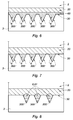
- the device 1 comprises successively the substrate 2, the metal layer 20, the filling material 6, the first layer 3, as illustrated in FIGS. Figures 6 to 8 .
- the alloy of the first and second layers 3, 5 and of the electroluminescent layer 4 is advantageously a binary alloy or a ternary alloy, the binary alloy preferably being based on GaN, the ternary alloy being preferably based on InGaN or AlGaN.
- the electroluminescent layer 4 may comprise electroluminescent sub-layers.
- the second layer 5 has an outer surface forming an interface with the output medium.
- the outer surface of the second layer 5 is advantageously textured in order to prevent a major part of the radiation produced from being trapped inside the device 1 by total internal reflections.
- the texturing of the outer surface of the second layer 5 is preferably obtained by a selective chemical attack based on KOH.
- the first and second layers 3, 5 and the electroluminescent layer 4 are preferably formed on an epitaxial growth substrate.
- the growth substrate is preferably sapphire when the spectral domain is visible; the growth substrate is preferably AlGaN when the spectral range is ultraviolet.
- the growth substrate is preferably removed by laser lift-off in the English language.
- the cavities 300 form inverted pyramid hollow patterns, generally hexagonal base (" V-pits " in English, the section being V-shaped). The peaks of the pyramids point to a dislocation or group of dislocations.
- the cavities 300 generally have a surface density between 10 8 and 10 10 cm -2 to the first surface 30 of the first layer 3. The Applicant has found that the total reflection, that is to say specular and diffuse, from radiation at the interface between the metal layer 20 and the first surface 30 of the first layer 3 decreases significantly from a surface density of the order of 10 8 cm -2 .
- the cavities 300 have a depth (that is to say the height of the pyramid) of the order of 150 nm, and a diameter (that is to say the diameter of the hexagon, substantially regular, forming the base of the pyramid) of the order of 100 nm.
- the filling material 6 forms a flat layer 60 extending between the metal layer 20 and the first surface 30 of the first layer 3, and the filling material 6 is electrically conductive.
- the filler material 6 is preferably an oxide, preferably selected from the group comprising indium tin oxide, zinc oxide ZnO doped with aluminum, indium or gallium. The doping level is adapted according to the desired level of conduction.
- the filling material 6 is deposited on the first surface 30 of the first layer 3 before the formation of the metal layer 20.
- the plane layer 60 is advantageously obtained by mechanical-chemical polishing.
- the flat layer 60 prevents any direct contact between the first layer 3 and the metal layer 20.
- the filling material 6 is flush with the first surface 30 of the first layer 3, and the first surface 30 of the first layer 3 is in contact with the metal layer 20.
- the filling material 6 is deposited on the first surface 30 of the first layer 3 before the formation of the metal layer 20. Then the outcropping is preferably obtained by mechano-chemical polishing of the filling material 6 to the first surface 30 of the first layer 3.
- the filling material 6 is advantageously selected from the group consisting of titanium dioxide TiO 2 , silicon dioxide SiO 2 , zinc oxide ZnO, zinc oxide ZnO doped with aluminum, silicon nitride SiN, indium oxide -tin.
- the metal layer 20 is in direct contact with the first layer 3 and the filling material 6.
- the filling material 6 forms dielectric balls 61, and the first surface 30 of the first layer 3 is in contact with the metal layer 20.
- dielectric beads 61 are advantageously formed by evaporation of a colloidal suspension, one of which example of implementation is given in the document T. Pinedo et al, "Assisted convective-capillary force assembly of gold colloids in a microfluid cell: Plasmonic properties of deterministic nanostructures", J. Vac. Sci. Technol., B 26 (6), 2008, p. 2513-2519 .
- This embodiment is advantageous because such a filling material 6 has a good flatness.
- Several dielectric balls 61 may also occupy a cavity 300.
- the dielectric beads 61 advantageously have a radius of between 2 nm and 20 nm so that the filling material 6 is projecting or withdrawn from the first surface 30 of the first layer 3 with a maximum distance of less than or equal to 10 nm.
- a roughness of the filling material 6 greater than 10 nm significantly degrades the reflection of the radiation at the interface between the filling material 6 and the metal layer 20. increasing absorption.
- such a radius of dielectric balls 61 much smaller than the size of the cavities 300, allows several dielectric beads 61 to occupy a cavity 300, which allows adaptation to different sizes of cavities 300.
- a dielectric ball size 61 as low as possible.
- the filler material 6 is advantageously selected from the group comprising titanium dioxide TiO 2 , silicon nitride SiN, silicon dioxide SiO 2 , zinc oxide ZnO.
Landscapes
- Led Devices (AREA)
- Electroluminescent Light Sources (AREA)
Applications Claiming Priority (1)
| Application Number | Priority Date | Filing Date | Title |
|---|---|---|---|
| FR1556152A FR3038451B1 (fr) | 2015-06-30 | 2015-06-30 | Dispositif electroluminescent. |
Publications (2)
| Publication Number | Publication Date |
|---|---|
| EP3113235A1 true EP3113235A1 (de) | 2017-01-04 |
| EP3113235B1 EP3113235B1 (de) | 2021-09-08 |
Family
ID=54478141
Family Applications (1)
| Application Number | Title | Priority Date | Filing Date |
|---|---|---|---|
| EP16176191.1A Active EP3113235B1 (de) | 2015-06-30 | 2016-06-24 | Elektrolumineszenzvorrichtung |
Country Status (3)
| Country | Link |
|---|---|
| US (1) | US10186636B2 (de) |
| EP (1) | EP3113235B1 (de) |
| FR (1) | FR3038451B1 (de) |
Cited By (1)
| Publication number | Priority date | Publication date | Assignee | Title |
|---|---|---|---|---|
| WO2021037457A1 (de) * | 2019-08-27 | 2021-03-04 | Osram Opto Semiconductors Gmbh | Halbleiterchip und verfahren zur herstellung eines halbleiterchips |
Families Citing this family (2)
| Publication number | Priority date | Publication date | Assignee | Title |
|---|---|---|---|---|
| DE102017105397A1 (de) | 2017-03-14 | 2018-09-20 | Osram Opto Semiconductors Gmbh | Verfahren zur Herstellung von Leuchtdioden und Leuchtdiode |
| WO2021090790A1 (ja) * | 2019-11-08 | 2021-05-14 | 出光興産株式会社 | 積層体及び半導体装置 |
Citations (5)
| Publication number | Priority date | Publication date | Assignee | Title |
|---|---|---|---|---|
| US6657236B1 (en) * | 1999-12-03 | 2003-12-02 | Cree Lighting Company | Enhanced light extraction in LEDs through the use of internal and external optical elements |
| US20080303047A1 (en) * | 2007-05-15 | 2008-12-11 | Epistar Corporation | Light-emitting diode device and manufacturing method therof |
| US20120280260A1 (en) * | 2008-11-17 | 2012-11-08 | Hyung Jo Park | Semiconductor light emitting device |
| US20120299040A1 (en) * | 2011-05-23 | 2012-11-29 | Samsung Electronics Co., Ltd. | Semiconductor light emitting device and method of manufacturing the same |
| US20140175474A1 (en) * | 2012-12-21 | 2014-06-26 | Samsung Electronics Co., Ltd. | Semiconductor light emitting device and method of manufacturing the same |
Family Cites Families (1)
| Publication number | Priority date | Publication date | Assignee | Title |
|---|---|---|---|---|
| US9508902B2 (en) * | 2005-02-21 | 2016-11-29 | Epistar Corporation | Optoelectronic semiconductor device |
-
2015
- 2015-06-30 FR FR1556152A patent/FR3038451B1/fr not_active Expired - Fee Related
-
2016
- 2016-06-24 EP EP16176191.1A patent/EP3113235B1/de active Active
- 2016-06-30 US US15/199,152 patent/US10186636B2/en active Active
Patent Citations (5)
| Publication number | Priority date | Publication date | Assignee | Title |
|---|---|---|---|---|
| US6657236B1 (en) * | 1999-12-03 | 2003-12-02 | Cree Lighting Company | Enhanced light extraction in LEDs through the use of internal and external optical elements |
| US20080303047A1 (en) * | 2007-05-15 | 2008-12-11 | Epistar Corporation | Light-emitting diode device and manufacturing method therof |
| US20120280260A1 (en) * | 2008-11-17 | 2012-11-08 | Hyung Jo Park | Semiconductor light emitting device |
| US20120299040A1 (en) * | 2011-05-23 | 2012-11-29 | Samsung Electronics Co., Ltd. | Semiconductor light emitting device and method of manufacturing the same |
| US20140175474A1 (en) * | 2012-12-21 | 2014-06-26 | Samsung Electronics Co., Ltd. | Semiconductor light emitting device and method of manufacturing the same |
Non-Patent Citations (2)
| Title |
|---|
| C.M. TSAI ET AL.: "Photonics Technology Letters", vol. 18, 2006, IEEE, article "High efficiency and improved ESD characteristics of GaN-based LEDs with naturally textured surface grown by MOCVD", pages: 1213 - 1215 |
| T. PINEDO ET AL.: "Assisted convective-capillary force assembly of gold colloids in a microfluid ce// : Plasmonic properties of deterministic nanostructures", J. VAC. SCI. TECHNOL., B, vol. 26, no. 6, 2008, pages 2513 - 2519, XP012114504, DOI: doi:10.1116/1.3021396 |
Cited By (2)
| Publication number | Priority date | Publication date | Assignee | Title |
|---|---|---|---|---|
| WO2021037457A1 (de) * | 2019-08-27 | 2021-03-04 | Osram Opto Semiconductors Gmbh | Halbleiterchip und verfahren zur herstellung eines halbleiterchips |
| US12261242B2 (en) | 2019-08-27 | 2025-03-25 | Osram Opto Semiconductors Gmbh | Semiconductor chip and method for producing a semiconductor chip |
Also Published As
| Publication number | Publication date |
|---|---|
| US10186636B2 (en) | 2019-01-22 |
| US20170005230A1 (en) | 2017-01-05 |
| FR3038451B1 (fr) | 2017-07-21 |
| EP3113235B1 (de) | 2021-09-08 |
| FR3038451A1 (fr) | 2017-01-06 |
Similar Documents
| Publication | Publication Date | Title |
|---|---|---|
| EP2203939B1 (de) | Optoelektronische anordnung mit nanodrähten und entsprechende verfahren | |
| EP2715808B1 (de) | Halbleiterstruktur zur ausstrahlung von licht und verfahren zur herstellung einer solchen struktur | |
| CN100565942C (zh) | 用于光电子学的半导体芯片及其制造方法 | |
| JP5623074B2 (ja) | 光電子半導体部品 | |
| EP3373345B1 (de) | Optoelektronische vorrichtung mit leuchtdioden mit verbesserter lichtextraktion | |
| FR3080487A1 (fr) | Procede de fabrication d’un dispositif optoelectronique a matrice de diodes | |
| FR2964796A1 (fr) | Dispositif optoelectronique a base de nanofils pour l'emission de lumiere | |
| FR2923651A1 (fr) | Procede de realisation d'une jonction pn dans un nanofil, et d'un nanofil avec au moins une jonction pn. | |
| FR2988904A1 (fr) | Structure semiconductrice optoelectronique a nanofils et procede de fabrication d'une telle structure | |
| WO2021130136A1 (fr) | Dispositif pour traitement par laser et procédé de traitement au laser | |
| EP3113235B1 (de) | Elektrolumineszenzvorrichtung | |
| EP3130010B1 (de) | Optoelektronische vorrichtung mit leuchtdioden und mit verbessertem emission diagramm | |
| CN100557835C (zh) | 用于光电子学的半导体芯片及其制造方法 | |
| EP3871255B1 (de) | Optoelektronische vorrichtung mit leuchtdioden mit verbesserter lichtextraktion und ein verfahren zu seiner herstellung | |
| EP2800151B1 (de) | Optoelektronische Anordnung, die mit einem Halbleiter-Nanodraht ausgestattet ist, dessen Längsabschnitt von einem Spiegelteil umgeben ist | |
| WO2013102664A1 (fr) | Substrat structure pour leds a forte extraction de lumiere | |
| EP3843162B1 (de) | Verfahren zur herstellung einer leuchtdiode mit einer extraktionsschicht, das einen dimensionierungsschritt einer halbleiterschicht umfasst | |
| EP2827390B1 (de) | Emissionsstruktur mit seitlicher Einspritzung von Trägerstoffen | |
| EP3843161B1 (de) | Verfahren zur herstellung einer leuchtdiode, das einen dimensionierungsschritt einer halbleiterschicht umfasst | |
| FR3137497A1 (fr) | Dispositif optoélectronique à réflecteur | |
| WO2021209460A1 (fr) | Procédé de fabrication d'un dispositif émetteur de rayonnement | |
| FR3105878A1 (fr) | Dispositif à composants optoélectroniques tridimensionnels pour découpe au laser et procédé de découpe au laser d'un tel dispositif |
Legal Events
| Date | Code | Title | Description |
|---|---|---|---|
| PUAI | Public reference made under article 153(3) epc to a published international application that has entered the european phase |
Free format text: ORIGINAL CODE: 0009012 |
|
| STAA | Information on the status of an ep patent application or granted ep patent |
Free format text: STATUS: EXAMINATION IS IN PROGRESS |
|
| 17P | Request for examination filed |
Effective date: 20160624 |
|
| AK | Designated contracting states |
Kind code of ref document: A1 Designated state(s): AL AT BE BG CH CY CZ DE DK EE ES FI FR GB GR HR HU IE IS IT LI LT LU LV MC MK MT NL NO PL PT RO RS SE SI SK SM TR |
|
| AX | Request for extension of the european patent |
Extension state: BA ME |
|
| RBV | Designated contracting states (corrected) |
Designated state(s): AL AT BE BG CH CY CZ DE DK EE ES FI FR GB GR HR HU IE IS IT LI LT LU LV MC MK MT NL NO PL PT RO RS SE SI SK SM TR |
|
| GRAP | Despatch of communication of intention to grant a patent |
Free format text: ORIGINAL CODE: EPIDOSNIGR1 |
|
| STAA | Information on the status of an ep patent application or granted ep patent |
Free format text: STATUS: GRANT OF PATENT IS INTENDED |
|
| INTG | Intention to grant announced |
Effective date: 20210407 |
|
| GRAS | Grant fee paid |
Free format text: ORIGINAL CODE: EPIDOSNIGR3 |
|
| GRAA | (expected) grant |
Free format text: ORIGINAL CODE: 0009210 |
|
| STAA | Information on the status of an ep patent application or granted ep patent |
Free format text: STATUS: THE PATENT HAS BEEN GRANTED |
|
| AK | Designated contracting states |
Kind code of ref document: B1 Designated state(s): AL AT BE BG CH CY CZ DE DK EE ES FI FR GB GR HR HU IE IS IT LI LT LU LV MC MK MT NL NO PL PT RO RS SE SI SK SM TR |
|
| REG | Reference to a national code |
Ref country code: GB Ref legal event code: FG4D Free format text: NOT ENGLISH |
|
| REG | Reference to a national code |
Ref country code: AT Ref legal event code: REF Ref document number: 1429358 Country of ref document: AT Kind code of ref document: T Effective date: 20210915 Ref country code: CH Ref legal event code: EP |
|
| REG | Reference to a national code |
Ref country code: IE Ref legal event code: FG4D Free format text: LANGUAGE OF EP DOCUMENT: FRENCH |
|
| REG | Reference to a national code |
Ref country code: DE Ref legal event code: R096 Ref document number: 602016063365 Country of ref document: DE |
|
| REG | Reference to a national code |
Ref country code: LT Ref legal event code: MG9D |
|
| REG | Reference to a national code |
Ref country code: NL Ref legal event code: MP Effective date: 20210908 |
|
| PG25 | Lapsed in a contracting state [announced via postgrant information from national office to epo] |
Ref country code: LT Free format text: LAPSE BECAUSE OF FAILURE TO SUBMIT A TRANSLATION OF THE DESCRIPTION OR TO PAY THE FEE WITHIN THE PRESCRIBED TIME-LIMIT Effective date: 20210908 Ref country code: BG Free format text: LAPSE BECAUSE OF FAILURE TO SUBMIT A TRANSLATION OF THE DESCRIPTION OR TO PAY THE FEE WITHIN THE PRESCRIBED TIME-LIMIT Effective date: 20211208 Ref country code: NO Free format text: LAPSE BECAUSE OF FAILURE TO SUBMIT A TRANSLATION OF THE DESCRIPTION OR TO PAY THE FEE WITHIN THE PRESCRIBED TIME-LIMIT Effective date: 20211208 Ref country code: FI Free format text: LAPSE BECAUSE OF FAILURE TO SUBMIT A TRANSLATION OF THE DESCRIPTION OR TO PAY THE FEE WITHIN THE PRESCRIBED TIME-LIMIT Effective date: 20210908 Ref country code: ES Free format text: LAPSE BECAUSE OF FAILURE TO SUBMIT A TRANSLATION OF THE DESCRIPTION OR TO PAY THE FEE WITHIN THE PRESCRIBED TIME-LIMIT Effective date: 20210908 Ref country code: SE Free format text: LAPSE BECAUSE OF FAILURE TO SUBMIT A TRANSLATION OF THE DESCRIPTION OR TO PAY THE FEE WITHIN THE PRESCRIBED TIME-LIMIT Effective date: 20210908 Ref country code: RS Free format text: LAPSE BECAUSE OF FAILURE TO SUBMIT A TRANSLATION OF THE DESCRIPTION OR TO PAY THE FEE WITHIN THE PRESCRIBED TIME-LIMIT Effective date: 20210908 Ref country code: HR Free format text: LAPSE BECAUSE OF FAILURE TO SUBMIT A TRANSLATION OF THE DESCRIPTION OR TO PAY THE FEE WITHIN THE PRESCRIBED TIME-LIMIT Effective date: 20210908 |
|
| REG | Reference to a national code |
Ref country code: AT Ref legal event code: MK05 Ref document number: 1429358 Country of ref document: AT Kind code of ref document: T Effective date: 20210908 |
|
| PG25 | Lapsed in a contracting state [announced via postgrant information from national office to epo] |
Ref country code: LV Free format text: LAPSE BECAUSE OF FAILURE TO SUBMIT A TRANSLATION OF THE DESCRIPTION OR TO PAY THE FEE WITHIN THE PRESCRIBED TIME-LIMIT Effective date: 20210908 Ref country code: GR Free format text: LAPSE BECAUSE OF FAILURE TO SUBMIT A TRANSLATION OF THE DESCRIPTION OR TO PAY THE FEE WITHIN THE PRESCRIBED TIME-LIMIT Effective date: 20211209 |
|
| PG25 | Lapsed in a contracting state [announced via postgrant information from national office to epo] |
Ref country code: AT Free format text: LAPSE BECAUSE OF FAILURE TO SUBMIT A TRANSLATION OF THE DESCRIPTION OR TO PAY THE FEE WITHIN THE PRESCRIBED TIME-LIMIT Effective date: 20210908 |
|
| PG25 | Lapsed in a contracting state [announced via postgrant information from national office to epo] |
Ref country code: IS Free format text: LAPSE BECAUSE OF FAILURE TO SUBMIT A TRANSLATION OF THE DESCRIPTION OR TO PAY THE FEE WITHIN THE PRESCRIBED TIME-LIMIT Effective date: 20220108 Ref country code: SM Free format text: LAPSE BECAUSE OF FAILURE TO SUBMIT A TRANSLATION OF THE DESCRIPTION OR TO PAY THE FEE WITHIN THE PRESCRIBED TIME-LIMIT Effective date: 20210908 Ref country code: SK Free format text: LAPSE BECAUSE OF FAILURE TO SUBMIT A TRANSLATION OF THE DESCRIPTION OR TO PAY THE FEE WITHIN THE PRESCRIBED TIME-LIMIT Effective date: 20210908 Ref country code: RO Free format text: LAPSE BECAUSE OF FAILURE TO SUBMIT A TRANSLATION OF THE DESCRIPTION OR TO PAY THE FEE WITHIN THE PRESCRIBED TIME-LIMIT Effective date: 20210908 Ref country code: PT Free format text: LAPSE BECAUSE OF FAILURE TO SUBMIT A TRANSLATION OF THE DESCRIPTION OR TO PAY THE FEE WITHIN THE PRESCRIBED TIME-LIMIT Effective date: 20220110 Ref country code: PL Free format text: LAPSE BECAUSE OF FAILURE TO SUBMIT A TRANSLATION OF THE DESCRIPTION OR TO PAY THE FEE WITHIN THE PRESCRIBED TIME-LIMIT Effective date: 20210908 Ref country code: NL Free format text: LAPSE BECAUSE OF FAILURE TO SUBMIT A TRANSLATION OF THE DESCRIPTION OR TO PAY THE FEE WITHIN THE PRESCRIBED TIME-LIMIT Effective date: 20210908 Ref country code: EE Free format text: LAPSE BECAUSE OF FAILURE TO SUBMIT A TRANSLATION OF THE DESCRIPTION OR TO PAY THE FEE WITHIN THE PRESCRIBED TIME-LIMIT Effective date: 20210908 Ref country code: CZ Free format text: LAPSE BECAUSE OF FAILURE TO SUBMIT A TRANSLATION OF THE DESCRIPTION OR TO PAY THE FEE WITHIN THE PRESCRIBED TIME-LIMIT Effective date: 20210908 Ref country code: AL Free format text: LAPSE BECAUSE OF FAILURE TO SUBMIT A TRANSLATION OF THE DESCRIPTION OR TO PAY THE FEE WITHIN THE PRESCRIBED TIME-LIMIT Effective date: 20210908 |
|
| REG | Reference to a national code |
Ref country code: DE Ref legal event code: R097 Ref document number: 602016063365 Country of ref document: DE |
|
| PLBE | No opposition filed within time limit |
Free format text: ORIGINAL CODE: 0009261 |
|
| STAA | Information on the status of an ep patent application or granted ep patent |
Free format text: STATUS: NO OPPOSITION FILED WITHIN TIME LIMIT |
|
| PG25 | Lapsed in a contracting state [announced via postgrant information from national office to epo] |
Ref country code: DK Free format text: LAPSE BECAUSE OF FAILURE TO SUBMIT A TRANSLATION OF THE DESCRIPTION OR TO PAY THE FEE WITHIN THE PRESCRIBED TIME-LIMIT Effective date: 20210908 |
|
| 26N | No opposition filed |
Effective date: 20220609 |
|
| PG25 | Lapsed in a contracting state [announced via postgrant information from national office to epo] |
Ref country code: SI Free format text: LAPSE BECAUSE OF FAILURE TO SUBMIT A TRANSLATION OF THE DESCRIPTION OR TO PAY THE FEE WITHIN THE PRESCRIBED TIME-LIMIT Effective date: 20210908 |
|
| PG25 | Lapsed in a contracting state [announced via postgrant information from national office to epo] |
Ref country code: MC Free format text: LAPSE BECAUSE OF FAILURE TO SUBMIT A TRANSLATION OF THE DESCRIPTION OR TO PAY THE FEE WITHIN THE PRESCRIBED TIME-LIMIT Effective date: 20210908 Ref country code: IT Free format text: LAPSE BECAUSE OF FAILURE TO SUBMIT A TRANSLATION OF THE DESCRIPTION OR TO PAY THE FEE WITHIN THE PRESCRIBED TIME-LIMIT Effective date: 20210908 |
|
| REG | Reference to a national code |
Ref country code: CH Ref legal event code: PL |
|
| REG | Reference to a national code |
Ref country code: BE Ref legal event code: MM Effective date: 20220630 |
|
| PG25 | Lapsed in a contracting state [announced via postgrant information from national office to epo] |
Ref country code: LU Free format text: LAPSE BECAUSE OF NON-PAYMENT OF DUE FEES Effective date: 20220624 Ref country code: LI Free format text: LAPSE BECAUSE OF NON-PAYMENT OF DUE FEES Effective date: 20220630 Ref country code: IE Free format text: LAPSE BECAUSE OF NON-PAYMENT OF DUE FEES Effective date: 20220624 Ref country code: CH Free format text: LAPSE BECAUSE OF NON-PAYMENT OF DUE FEES Effective date: 20220630 |
|
| PG25 | Lapsed in a contracting state [announced via postgrant information from national office to epo] |
Ref country code: BE Free format text: LAPSE BECAUSE OF NON-PAYMENT OF DUE FEES Effective date: 20220630 |
|
| PG25 | Lapsed in a contracting state [announced via postgrant information from national office to epo] |
Ref country code: HU Free format text: LAPSE BECAUSE OF FAILURE TO SUBMIT A TRANSLATION OF THE DESCRIPTION OR TO PAY THE FEE WITHIN THE PRESCRIBED TIME-LIMIT; INVALID AB INITIO Effective date: 20160624 |
|
| PG25 | Lapsed in a contracting state [announced via postgrant information from national office to epo] |
Ref country code: MK Free format text: LAPSE BECAUSE OF FAILURE TO SUBMIT A TRANSLATION OF THE DESCRIPTION OR TO PAY THE FEE WITHIN THE PRESCRIBED TIME-LIMIT Effective date: 20210908 Ref country code: CY Free format text: LAPSE BECAUSE OF FAILURE TO SUBMIT A TRANSLATION OF THE DESCRIPTION OR TO PAY THE FEE WITHIN THE PRESCRIBED TIME-LIMIT Effective date: 20210908 |
|
| PG25 | Lapsed in a contracting state [announced via postgrant information from national office to epo] |
Ref country code: MT Free format text: LAPSE BECAUSE OF FAILURE TO SUBMIT A TRANSLATION OF THE DESCRIPTION OR TO PAY THE FEE WITHIN THE PRESCRIBED TIME-LIMIT Effective date: 20210908 |
|
| REG | Reference to a national code |
Ref country code: DE Ref legal event code: R079 Ref document number: 602016063365 Country of ref document: DE Free format text: PREVIOUS MAIN CLASS: H01L0033200000 Ipc: H10H0020819000 |
|
| PGFP | Annual fee paid to national office [announced via postgrant information from national office to epo] |
Ref country code: DE Payment date: 20250618 Year of fee payment: 10 |
|
| PGFP | Annual fee paid to national office [announced via postgrant information from national office to epo] |
Ref country code: GB Payment date: 20250625 Year of fee payment: 10 |
|
| PGFP | Annual fee paid to national office [announced via postgrant information from national office to epo] |
Ref country code: FR Payment date: 20250623 Year of fee payment: 10 |
|
| PG25 | Lapsed in a contracting state [announced via postgrant information from national office to epo] |
Ref country code: TR Free format text: LAPSE BECAUSE OF FAILURE TO SUBMIT A TRANSLATION OF THE DESCRIPTION OR TO PAY THE FEE WITHIN THE PRESCRIBED TIME-LIMIT Effective date: 20210908 |