EP3113345B1 - Convertisseur électrique et procédé de commande - Google Patents
Convertisseur électrique et procédé de commande Download PDFInfo
- Publication number
- EP3113345B1 EP3113345B1 EP15174720.1A EP15174720A EP3113345B1 EP 3113345 B1 EP3113345 B1 EP 3113345B1 EP 15174720 A EP15174720 A EP 15174720A EP 3113345 B1 EP3113345 B1 EP 3113345B1
- Authority
- EP
- European Patent Office
- Prior art keywords
- voltage
- phase
- converter
- input
- electrical converter
- Prior art date
- Legal status (The legal status is an assumption and is not a legal conclusion. Google has not performed a legal analysis and makes no representation as to the accuracy of the status listed.)
- Active
Links
Images






Classifications
-
- H—ELECTRICITY
- H02—GENERATION; CONVERSION OR DISTRIBUTION OF ELECTRIC POWER
- H02M—APPARATUS FOR CONVERSION BETWEEN AC AND AC, BETWEEN AC AND DC, OR BETWEEN DC AND DC, AND FOR USE WITH MAINS OR SIMILAR POWER SUPPLY SYSTEMS; CONVERSION OF DC OR AC INPUT POWER INTO SURGE OUTPUT POWER; CONTROL OR REGULATION THEREOF
- H02M1/00—Details of apparatus for conversion
- H02M1/42—Circuits or arrangements for compensating for or adjusting power factor in converters or inverters
- H02M1/4208—Arrangements for improving power factor of AC input
- H02M1/4216—Arrangements for improving power factor of AC input operating from a three-phase input voltage
-
- H—ELECTRICITY
- H02—GENERATION; CONVERSION OR DISTRIBUTION OF ELECTRIC POWER
- H02M—APPARATUS FOR CONVERSION BETWEEN AC AND AC, BETWEEN AC AND DC, OR BETWEEN DC AND DC, AND FOR USE WITH MAINS OR SIMILAR POWER SUPPLY SYSTEMS; CONVERSION OF DC OR AC INPUT POWER INTO SURGE OUTPUT POWER; CONTROL OR REGULATION THEREOF
- H02M1/00—Details of apparatus for conversion
- H02M1/12—Arrangements for reducing harmonics from AC input or output
-
- H—ELECTRICITY
- H02—GENERATION; CONVERSION OR DISTRIBUTION OF ELECTRIC POWER
- H02M—APPARATUS FOR CONVERSION BETWEEN AC AND AC, BETWEEN AC AND DC, OR BETWEEN DC AND DC, AND FOR USE WITH MAINS OR SIMILAR POWER SUPPLY SYSTEMS; CONVERSION OF DC OR AC INPUT POWER INTO SURGE OUTPUT POWER; CONTROL OR REGULATION THEREOF
- H02M3/00—Conversion of DC power input into DC power output
- H02M3/02—Conversion of DC power input into DC power output without intermediate conversion into AC
- H02M3/04—Conversion of DC power input into DC power output without intermediate conversion into AC by static converters
- H02M3/10—Conversion of DC power input into DC power output without intermediate conversion into AC by static converters using discharge tubes with control electrode or semiconductor devices with control electrode
- H02M3/145—Conversion of DC power input into DC power output without intermediate conversion into AC by static converters using discharge tubes with control electrode or semiconductor devices with control electrode using devices of a triode or transistor type requiring continuous application of a control signal
- H02M3/155—Conversion of DC power input into DC power output without intermediate conversion into AC by static converters using discharge tubes with control electrode or semiconductor devices with control electrode using devices of a triode or transistor type requiring continuous application of a control signal using semiconductor devices only
- H02M3/156—Conversion of DC power input into DC power output without intermediate conversion into AC by static converters using discharge tubes with control electrode or semiconductor devices with control electrode using devices of a triode or transistor type requiring continuous application of a control signal using semiconductor devices only with automatic control of output voltage or current, e.g. switching regulators
- H02M3/158—Conversion of DC power input into DC power output without intermediate conversion into AC by static converters using discharge tubes with control electrode or semiconductor devices with control electrode using devices of a triode or transistor type requiring continuous application of a control signal using semiconductor devices only with automatic control of output voltage or current, e.g. switching regulators including plural semiconductor devices as final control devices for a single load
-
- H—ELECTRICITY
- H02—GENERATION; CONVERSION OR DISTRIBUTION OF ELECTRIC POWER
- H02M—APPARATUS FOR CONVERSION BETWEEN AC AND AC, BETWEEN AC AND DC, OR BETWEEN DC AND DC, AND FOR USE WITH MAINS OR SIMILAR POWER SUPPLY SYSTEMS; CONVERSION OF DC OR AC INPUT POWER INTO SURGE OUTPUT POWER; CONTROL OR REGULATION THEREOF
- H02M7/00—Conversion of AC power input into DC power output; Conversion of DC power input into AC power output
- H02M7/02—Conversion of AC power input into DC power output without possibility of reversal
- H02M7/04—Conversion of AC power input into DC power output without possibility of reversal by static converters
- H02M7/06—Conversion of AC power input into DC power output without possibility of reversal by static converters using discharge tubes without control electrode or semiconductor devices without control electrode
-
- H—ELECTRICITY
- H02—GENERATION; CONVERSION OR DISTRIBUTION OF ELECTRIC POWER
- H02M—APPARATUS FOR CONVERSION BETWEEN AC AND AC, BETWEEN AC AND DC, OR BETWEEN DC AND DC, AND FOR USE WITH MAINS OR SIMILAR POWER SUPPLY SYSTEMS; CONVERSION OF DC OR AC INPUT POWER INTO SURGE OUTPUT POWER; CONTROL OR REGULATION THEREOF
- H02M7/00—Conversion of AC power input into DC power output; Conversion of DC power input into AC power output
- H02M7/02—Conversion of AC power input into DC power output without possibility of reversal
- H02M7/04—Conversion of AC power input into DC power output without possibility of reversal by static converters
- H02M7/12—Conversion of AC power input into DC power output without possibility of reversal by static converters using discharge tubes with control electrode or semiconductor devices with control electrode
- H02M7/21—Conversion of AC power input into DC power output without possibility of reversal by static converters using discharge tubes with control electrode or semiconductor devices with control electrode using devices of a triode or transistor type requiring continuous application of a control signal
- H02M7/217—Conversion of AC power input into DC power output without possibility of reversal by static converters using discharge tubes with control electrode or semiconductor devices with control electrode using devices of a triode or transistor type requiring continuous application of a control signal using semiconductor devices only
-
- H—ELECTRICITY
- H02—GENERATION; CONVERSION OR DISTRIBUTION OF ELECTRIC POWER
- H02M—APPARATUS FOR CONVERSION BETWEEN AC AND AC, BETWEEN AC AND DC, OR BETWEEN DC AND DC, AND FOR USE WITH MAINS OR SIMILAR POWER SUPPLY SYSTEMS; CONVERSION OF DC OR AC INPUT POWER INTO SURGE OUTPUT POWER; CONTROL OR REGULATION THEREOF
- H02M7/00—Conversion of AC power input into DC power output; Conversion of DC power input into AC power output
- H02M7/42—Conversion of DC power input into AC power output without possibility of reversal
- H02M7/44—Conversion of DC power input into AC power output without possibility of reversal by static converters
- H02M7/48—Conversion of DC power input into AC power output without possibility of reversal by static converters using discharge tubes with control electrode or semiconductor devices with control electrode
- H02M7/483—Converters with outputs that each can have more than two voltages levels
-
- H—ELECTRICITY
- H02—GENERATION; CONVERSION OR DISTRIBUTION OF ELECTRIC POWER
- H02M—APPARATUS FOR CONVERSION BETWEEN AC AND AC, BETWEEN AC AND DC, OR BETWEEN DC AND DC, AND FOR USE WITH MAINS OR SIMILAR POWER SUPPLY SYSTEMS; CONVERSION OF DC OR AC INPUT POWER INTO SURGE OUTPUT POWER; CONTROL OR REGULATION THEREOF
- H02M1/00—Details of apparatus for conversion
- H02M1/0067—Converter structures employing plural converter units, other than for parallel operation of the units on a single load
- H02M1/007—Plural converter units in cascade
-
- H—ELECTRICITY
- H02—GENERATION; CONVERSION OR DISTRIBUTION OF ELECTRIC POWER
- H02M—APPARATUS FOR CONVERSION BETWEEN AC AND AC, BETWEEN AC AND DC, OR BETWEEN DC AND DC, AND FOR USE WITH MAINS OR SIMILAR POWER SUPPLY SYSTEMS; CONVERSION OF DC OR AC INPUT POWER INTO SURGE OUTPUT POWER; CONTROL OR REGULATION THEREOF
- H02M3/00—Conversion of DC power input into DC power output
- H02M3/005—Conversion of DC power input into DC power output using Cuk converters
-
- H—ELECTRICITY
- H02—GENERATION; CONVERSION OR DISTRIBUTION OF ELECTRIC POWER
- H02M—APPARATUS FOR CONVERSION BETWEEN AC AND AC, BETWEEN AC AND DC, OR BETWEEN DC AND DC, AND FOR USE WITH MAINS OR SIMILAR POWER SUPPLY SYSTEMS; CONVERSION OF DC OR AC INPUT POWER INTO SURGE OUTPUT POWER; CONTROL OR REGULATION THEREOF
- H02M3/00—Conversion of DC power input into DC power output
- H02M3/02—Conversion of DC power input into DC power output without intermediate conversion into AC
- H02M3/04—Conversion of DC power input into DC power output without intermediate conversion into AC by static converters
- H02M3/10—Conversion of DC power input into DC power output without intermediate conversion into AC by static converters using discharge tubes with control electrode or semiconductor devices with control electrode
- H02M3/145—Conversion of DC power input into DC power output without intermediate conversion into AC by static converters using discharge tubes with control electrode or semiconductor devices with control electrode using devices of a triode or transistor type requiring continuous application of a control signal
- H02M3/155—Conversion of DC power input into DC power output without intermediate conversion into AC by static converters using discharge tubes with control electrode or semiconductor devices with control electrode using devices of a triode or transistor type requiring continuous application of a control signal using semiconductor devices only
- H02M3/1557—Single ended primary inductor converters [SEPIC]
-
- H—ELECTRICITY
- H02—GENERATION; CONVERSION OR DISTRIBUTION OF ELECTRIC POWER
- H02M—APPARATUS FOR CONVERSION BETWEEN AC AND AC, BETWEEN AC AND DC, OR BETWEEN DC AND DC, AND FOR USE WITH MAINS OR SIMILAR POWER SUPPLY SYSTEMS; CONVERSION OF DC OR AC INPUT POWER INTO SURGE OUTPUT POWER; CONTROL OR REGULATION THEREOF
- H02M3/00—Conversion of DC power input into DC power output
- H02M3/22—Conversion of DC power input into DC power output with intermediate conversion into AC
- H02M3/24—Conversion of DC power input into DC power output with intermediate conversion into AC by static converters
- H02M3/28—Conversion of DC power input into DC power output with intermediate conversion into AC by static converters using discharge tubes with control electrode or semiconductor devices with control electrode to produce the intermediate AC
- H02M3/325—Conversion of DC power input into DC power output with intermediate conversion into AC by static converters using discharge tubes with control electrode or semiconductor devices with control electrode to produce the intermediate AC using devices of a triode or a transistor type requiring continuous application of a control signal
- H02M3/335—Conversion of DC power input into DC power output with intermediate conversion into AC by static converters using discharge tubes with control electrode or semiconductor devices with control electrode to produce the intermediate AC using devices of a triode or a transistor type requiring continuous application of a control signal using semiconductor devices only
- H02M3/3353—Conversion of DC power input into DC power output with intermediate conversion into AC by static converters using discharge tubes with control electrode or semiconductor devices with control electrode to produce the intermediate AC using devices of a triode or a transistor type requiring continuous application of a control signal using semiconductor devices only having at least two simultaneously operating switches on the input side, e.g. "double forward" or "double (switched) flyback" converter
-
- H—ELECTRICITY
- H02—GENERATION; CONVERSION OR DISTRIBUTION OF ELECTRIC POWER
- H02M—APPARATUS FOR CONVERSION BETWEEN AC AND AC, BETWEEN AC AND DC, OR BETWEEN DC AND DC, AND FOR USE WITH MAINS OR SIMILAR POWER SUPPLY SYSTEMS; CONVERSION OF DC OR AC INPUT POWER INTO SURGE OUTPUT POWER; CONTROL OR REGULATION THEREOF
- H02M3/00—Conversion of DC power input into DC power output
- H02M3/22—Conversion of DC power input into DC power output with intermediate conversion into AC
- H02M3/24—Conversion of DC power input into DC power output with intermediate conversion into AC by static converters
- H02M3/28—Conversion of DC power input into DC power output with intermediate conversion into AC by static converters using discharge tubes with control electrode or semiconductor devices with control electrode to produce the intermediate AC
- H02M3/325—Conversion of DC power input into DC power output with intermediate conversion into AC by static converters using discharge tubes with control electrode or semiconductor devices with control electrode to produce the intermediate AC using devices of a triode or a transistor type requiring continuous application of a control signal
- H02M3/335—Conversion of DC power input into DC power output with intermediate conversion into AC by static converters using discharge tubes with control electrode or semiconductor devices with control electrode to produce the intermediate AC using devices of a triode or a transistor type requiring continuous application of a control signal using semiconductor devices only
- H02M3/33569—Conversion of DC power input into DC power output with intermediate conversion into AC by static converters using discharge tubes with control electrode or semiconductor devices with control electrode to produce the intermediate AC using devices of a triode or a transistor type requiring continuous application of a control signal using semiconductor devices only having several active switching elements
- H02M3/33576—Conversion of DC power input into DC power output with intermediate conversion into AC by static converters using discharge tubes with control electrode or semiconductor devices with control electrode to produce the intermediate AC using devices of a triode or a transistor type requiring continuous application of a control signal using semiconductor devices only having several active switching elements having at least one active switching element at the secondary side of an isolation transformer
-
- H—ELECTRICITY
- H02—GENERATION; CONVERSION OR DISTRIBUTION OF ELECTRIC POWER
- H02M—APPARATUS FOR CONVERSION BETWEEN AC AND AC, BETWEEN AC AND DC, OR BETWEEN DC AND DC, AND FOR USE WITH MAINS OR SIMILAR POWER SUPPLY SYSTEMS; CONVERSION OF DC OR AC INPUT POWER INTO SURGE OUTPUT POWER; CONTROL OR REGULATION THEREOF
- H02M7/00—Conversion of AC power input into DC power output; Conversion of DC power input into AC power output
- H02M7/42—Conversion of DC power input into AC power output without possibility of reversal
- H02M7/44—Conversion of DC power input into AC power output without possibility of reversal by static converters
- H02M7/48—Conversion of DC power input into AC power output without possibility of reversal by static converters using discharge tubes with control electrode or semiconductor devices with control electrode
- H02M7/483—Converters with outputs that each can have more than two voltages levels
- H02M7/487—Neutral point clamped inverters
-
- Y—GENERAL TAGGING OF NEW TECHNOLOGICAL DEVELOPMENTS; GENERAL TAGGING OF CROSS-SECTIONAL TECHNOLOGIES SPANNING OVER SEVERAL SECTIONS OF THE IPC; TECHNICAL SUBJECTS COVERED BY FORMER USPC CROSS-REFERENCE ART COLLECTIONS [XRACs] AND DIGESTS
- Y02—TECHNOLOGIES OR APPLICATIONS FOR MITIGATION OR ADAPTATION AGAINST CLIMATE CHANGE
- Y02B—CLIMATE CHANGE MITIGATION TECHNOLOGIES RELATED TO BUILDINGS, e.g. HOUSING, HOUSE APPLIANCES OR RELATED END-USER APPLICATIONS
- Y02B70/00—Technologies for an efficient end-user side electric power management and consumption
- Y02B70/10—Technologies improving the efficiency by using switched-mode power supplies [SMPS], i.e. efficient power electronics conversion e.g. power factor correction or reduction of losses in power supplies or efficient standby modes
Definitions
- the invention relates to the field of current conversion.
- the invention relates to an electrical converter and a method for controlling the electrical converter.
- an electrical converter may convert a three-phase AC voltage and may supply it to a DC bus, to which several batteries may be connected. Also data centres and telco sites usually need such an AC-to-DC conversion.
- low voltage (about 400 V) DC distribution systems and DC micro grids typically require AC-to-DC conversion from an existing AC electrical grid.
- Such electrical converters may comprise a boost-type power factor correction (PFC) stage with a 700V - 800V DC output connected in series with a DC-DC converter to achieve the desired lower DC bus voltage.
- PFC boost-type power factor correction
- Buck-type PFC converters are an alternative, allowing a single-stage energy conversion between the three-phase mains and a DC bus with lower voltage.
- CH 704 553 A2 shows a hybrid three-phase AC/DC converter with a three-phase bridge circuit and a four-quadrant switch, which are interconnected via a lower, intermediate and upper interconnection point with an output converter.
- An input filter comprises three star-connected capacitors.
- An aspect of the invention relates to an electrical converter, which, for example may be used for converting a three-phase AC voltage from an electrical grid (which may be a medium voltage, i.e. more than 1.000 kV into a low AC or DC output voltage, i.e. below 1.000 kV).
- an electrical grid which may be a medium voltage, i.e. more than 1.000 kV into a low AC or DC output voltage, i.e. below 1.000 kV).
- the electrical converter comprises an input voltage selector for converting a three-phase AC input voltage provided at three phase inputs of the electrical converter into an intermediate three-phase voltage provided at an upper voltage node, a middle voltage node and a lower voltage node; capacitors interconnecting an upper voltage node, a middle voltage node and a lower voltage node; and an output converter for converting the intermediate three-phase voltage into an output voltage.
- the input voltage selector which may be seen as a first converter stage, is adapted for connecting the upper voltage node to a phase input with the highest voltage of the three-phase AC input voltage, the lower voltage node to a phase input with the lowest voltage of the three-phase AC input voltage, and the middle voltage node to the phase input having a voltage between the highest voltage and the lowest voltage.
- the input voltage selector may convert the three sinusoidal AC input voltages into three piece-wise sinusoidal voltages provided at the upper voltage, middle voltage and lower voltage node.
- the output converter which may be seen as a second converter stage and/or which may have different topologies (see below) may convert these piece-wise sinusoidal voltages into a DC voltage or a further AC voltage of different voltage magnitude and/or different frequency.
- capacitors are arranged between the input voltage selector and the output converter. These capacitors may be seen as (a part of) an input filter for the output converter. These capacitors may interconnect the upper voltage, middle voltage and lower voltage node.
- the capacitors are arranged behind (and not before) the input voltage selector from the point of the view of the phase inputs of the electrical converter (and an electrical grid connected to these phase inputs), the current distortions at the intersection of phase voltages in the phase inputs, which are mainly caused by switching voltage ripples across the capacitors, may be better controlled.
- the electrical converter is controlled such that the current distortions caused by the switching of the output converter are suppressed by switching the input voltage selector in a specific way, when two of the phase voltages in the phase inputs cross.
- the upper voltage node, the middle voltage node and the lower voltage node are star-connected and/or are delta-connected via the capacitors.
- Each node may be directly connected via a capacitor with both of the other nodes or may be connected with a capacitor via a star-point with the other nodes.
- a filter inductor is interconnected in each phase input.
- These filter inductors and the capacitors may be seen as parts of a (split) LC-filter before the input of the output converter.
- the input voltage selector may be seen as interconnected in this electrical filter.
- each of the upper voltage node, the middle voltage node and the lower voltage node is connected via a filter inductor with the capacitors interconnecting the upper voltage node, the middle voltage node and the lower voltage node.
- the input voltage selector may be designed to achieve the above-mentioned distribution of the three sinusoidal AC input voltages into the three piece-wise sinusoidal voltages provided at the high, middle and lower voltage node.
- the input voltage selector comprises three selector legs for interconnecting one of the phase inputs with the upper voltage node, the middle voltage node and the lower voltage node, each selector leg comprising a half-bridge and an injector switch unit, the half-bridge connected to the upper voltage node and lower voltage node and the injector switch unit connected to the middle voltage node.
- each selector leg may comprise two half-bridges in parallel.
- the half-bridge comprises diodes and/or the half-bridge comprises controllable semiconductor switches.
- the half-bridge may be a diode-half-bridge.
- these diodes may have to be substituted with semiconductor switches to allow a power transfer towards the phase inputs.
- phase inputs are connected with the injector switch unit.
- the injector switch unit comprises two series-connected semiconductor switches, which are reverse to each other, the injector switch unit comprises one controllable semiconductor switch interconnected in parallel with two pairs of two series-connected diodes and/or the injector switch unit comprises a half-bridge of diodes and/or controllable semiconductor switches.
- the injector switch unit interconnects a middle point of the half-bridge with the middle voltage node or the injector switch unit is interconnected between arms of the half-bridge.
- the output converter is a DC-to-DC converter or a DC-to-AC converter.
- the output converter may be adapted for converting the piece-wise sinusoidal voltage provided at the nodes at the output of the input selector in a DC voltage or into a possibly multi-phase AC voltage.
- the electrical converter may be used for DC-distribution systems, datacenter and battery charging.
- the output converter may have many possible topologies, for example, it may be or may comprise at least one of: a simple buck or boost converter, a buck-boost converter, a non-inverting buck-boost converter, a SEPIC converter, a Cuk converter, an inverting buck-boost converter, and/or interleaved buck or boost converters.
- the output converter comprises three-level half-bridges; and/or wherein the half-bridges are NPC based or T-type based.
- the output converter is an isolated output converter comprising a transformer between two subconverter units.
- a common mode filter is provided at an output of the output converter.
- the output converter may have two DC outputs, which may be coupled with a common mode inductor and/or a common mode capacitor.
- a star-point of the capacitors interconnecting the upper voltage node, the middle voltage node and the lower voltage node is connected with the common mode filter.
- the common mode filter may comprise two series connected common mode capacitors, which are interconnecting two outputs of the output converter. The point between the two capacitors may be connected to the star-point of the capacitors interconnecting the upper voltage node, the middle voltage node and the lower voltage node.
- a further aspect of the invention relates to a method for controlling an electrical converter as described in the above and in the following.
- the method is performed by a controller, which based on measurements in the electrical converter determines switching instants of semiconductor switches of the electrical converter.
- the measurements may provide information on currents as input currents, intermediate currents and/or output currents as well as voltages, such as input (grid) voltages, intermediate voltages, capacitor voltages and/or output voltages in the electrical converter.
- the method comprises: switching semiconductor switches of the input voltage selector such that the upper voltage node is connected to the phase input with the highest voltage of the three-phase AC input voltage, the lower voltage node is connected to the phase input with the lowest voltage of the three-phase AC input voltage, and the middle voltage node is connected to the phase input with a voltage between the highest voltage and the lowest voltage; wherein, when two of the voltages of the three-phase AC input voltage are crossing, the semiconductor switches of the input voltage selector are switched such that the corresponding two phase inputs are short-circuited for a specific duration in order to lower current distortions in the phase inputs of the electrical converter.
- the controller switches the semiconductor switches of the input voltage selector, such that the highest, intermediate and lowest voltage provided at the phase inputs (for example by an electrical grid) is provided to the highest voltage node, middle voltage node and lowest voltage node.
- the controller may switch semiconductor switches of the output converter (for example with a PWM scheme) such that the (piece-wise sinusoidal) voltages at the nodes are converted into a DC or AC output voltage.
- the input voltage selector may be used to mitigate current distortions at the phase inputs of the electrical converter.
- the controller switches semiconductor switches of the input voltage selector such that during the crossing of the input phases, the phase inputs of the crossing phases are short circuited, which may cancel at least partially the current distortions.
- the crossing of phases not only may relate to the point, where the two phase voltages are equal but also to the vicinity of this point, for example a time interval.
- the electrical converter comprises phase inductors, each phase inductor interconnected between a phase input of the electrical converter and a respective phase input of the input voltage selector, wherein the two phase inputs of the electrical converter and the corresponding phase inductors are short-circuited such that a voltage average of a voltage between the corresponding phase inputs of the input voltage selector equals a grid voltage provided between the two phase inputs of the electrical converter.
- the electrical converter comprises phase inductors at its phase inputs, which together with the capacitors at the output of the input voltage selector may form a split electrical filter.
- the voltages at the phase inputs of the electrical converter may equalize via the phase inductors in such a way that a current reverse to a current distortion is generated, which mitigates the current distortion.
- the specific duration, during which the two phase inputs are short-circuited is determined such that during each switching cycle of a PWM modulation scheme of the output converter, the voltage average equals a grid voltage provided between the two phase inputs of the electrical converter.
- the short-circuiting takes place every switching cycle, i.e. the corresponding switch of the input voltage selector is toggled on and off every switching cycle.
- the time at which the two phase inputs are short-circuited is determined based on a time, at which a semiconductor switch of an output side DC-DC converter is switched based on a PWM modulation scheme.
- the switching time is not determined on the beginning of the switching cycle but on the switching time of the output converter.
- the electrical converter is a bidirectional converter, also a power transfer in the reverse direction is possible and current distortions may be mitigated by correspondingly switching semiconductor switches of the input voltage selector.
- Fig. 1 shows an electrical converter 10 comprising two converter stages 12, 14 in the form of an input voltage selector 12 and an output converter 14.
- the electrical converter 10 of Fig. 1 is an AC-to-DC converter having three phase inputs a, b, c for connecting to an electrical grid and two DC outputs p, n, which for example may be connected with a DC bus bar of a battery charging station.
- the input voltage selector 12 also has three phase inputs a , b , c , which are interconnected via the phase inductors L f with the phase inputs a, b, c, and three outputs x, y, z. These outputs may be seen as an upper voltage node x, a middle voltage node y and a lower voltage node z.
- the input voltage selector 12 connects the upper voltage node x to the phase input a, b, c with the highest voltage of the three-phase AC input voltage, the lower voltage node z to a phase input a, b, c with the lowest voltage of the three-phase AC input voltage, and the middle voltage node y to the phase input a, b, c having a voltage between the highest voltage and the lowest voltage.
- the input voltage selector 12 comprises three selector legs 16, each of which interconnects one of the phase inputs a , b , c with the nodes x, y, z.
- Each selector leg 16 comprises a half-bridge 18 (in case of Fig. 1 of diodes) interconnecting the nodes x and z, and an injector switch unit 20 (S aya , S byb and S cyc ) connected to the node y.
- the outputs x, y, z of the input voltage selector 16 are the inputs of the output converter 14, which in the embodiment of Fig.1 comprises two DC-DC buck converters and a DC output capacitor C pn .
- the switches of the output converter 14 pare switched with a PWM (pulse width modulation) scheme to generate a DC voltage between the outputs p, n.
- Three AC capacitors C x , C y , C z are connected between the nodes x, y, z. Note that in Fig. 1 , the capacitors C x , C y , C z are star-connected, while in Fig. 2 the capacitors C x , C y , C z are delta-connected. However, a delta-connection is also possible in Fig. 1 or a star-connection in Fig. 2 . In general, the three capacitors C x , C y , C z should have equal capacitance, in order to symmetrically load the AC grid. This may be required as the voltages at nodes x, y and z are piece-wise sinusoidal and form a three-phase system within every 60° sector of the AC input voltage.
- phase inductors and the capacitors C x , C y , C z may be seen as an electrical filter that is split into two parts by the input voltage selector 12.
- the structure of the proposed circuit with the capacitors on the output side of the input voltage selector 12 has several advantages: It shortens the commutation loops of the output converters 14, which means that no additional capacitors are required. Furthermore, the currents i x , i y and i z flowing through the input voltage selector 12 are continuous with these filter capacitors C x , C y , C z . This leads to a reduction of conduction losses in the switches of the input voltage selector 12. Additionally, the capacitors decouple the switching operations of the input voltage selector 12 and the output converter 14. Finally, in the proposed circuit, the distortions in the AC side input currents i a , i b and i c can be prevented by properly modulating the switches in the input voltage selector 12 as described below and above.
- Fig. 1 shows a unidirectional converter 10
- Fig. 2 shows a bidirectional converter 10, in which the diodes in the input voltage selector 12 and the output converter 14 have been supplemented with controllable semiconductor switches.
- a full bidirectional solution may be obtained by connecting active switches in parallel with the diodes and by connecting diodes in parallel with the existent active switches.
- the outputs x, y, z of the input voltage selector 12 are connected via inductors L f with the capacitors C x , C y , C z .
- the whole electrical LC filter may be arranged between the input voltage selector 12 and the output converter.
- Fig. 3A, 3B , 3C, 3D show different variants of a unidirectional input voltage selector 12a, 12b, 12c, 12d, which may be used in Fig. 1 .
- 12a and 12c may be made bidirectional by connecting active switches in parallel with the diodes Dax, Dbx, Dcx, Dza, Dzb and Dzc.
- the injector switch unit 20 is connected via a middle point of the respective half-bridge 18 with the node y. In the input selector 12b, the injector switch unit 20 is integrated into the respective half-bridge 18.
- the injector switch units 20 of Fig. 1 and 2 have two switches connected in antiseries
- the injector switch units 20 of Fig. 3A and 3B have one switch interconnected with four diodes.
- Fig. 3C and 3D show input voltage selector 12c and 12d with a further half-bridge used as injector switch unit 20 per selector leg 16.
- an active half-bridge 18 is connected to the phase input, while a passive (diode) half-bridge 20 is connected to the middle voltage node y.
- Fig. 3D is vice versa.
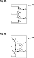
- Fig. 4A to 4D show further embodiments 14a to 14f for the output converter stage providing a DC output voltage at outputs p, n.
- a full bidirectional converter 10 may be obtained by connecting active switches in parallel with the circuit diodes and by connecting diodes in parallel with the existent active switches.
- the output converter 14 may be or may comprise a boost converter 14a, a non-inverting boost converter 14b, a SEPIC converter 14c, a Cuk converter 14d with inversed output voltage, an inverting buck-boost converter 14e with reversed output voltage, and/or two interleaved buck converters 14f.
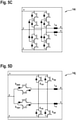
- Fig. 5A to 5D show further embodiments 14g to 14j for the output converter stage providing a DC output voltage at outputs p, n based on three-level circuit topologies.
- the output converters 14g and 14h support AC-to-DC power transfer only, which means that if the output power is reversed, the load current has to be reversed as well. If additional diodes are added as shown with output converters 14i and 14j, bidirectional power transfer is possible, provided a bidirectional input voltage selector 12 is also used.
- Output converters 14g and 14i are NPC (neutral point clamped) based, while 14h and 14j are T-type based.
- the output converters 14a to 14j are all non-isolating.
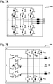
- Fig. 6A and 6B show isolating output converters 14k, 141, which comprise an isolating transformer 22 between two subconverters 24.
- output converter 14k an NPC based full-bridge configuration and in output converter 141 a T-type configuration of switches on the transformer's primary side are used.
- an active conventional full-bridge circuit is implemented, however, a simple diode bridge also may be implemented.
- the secondary side circuit 24 such as current doubler, voltage doubler, etc. may be used.
- the secondary side circuit may be like the ones shown in Fig. 6A or 6B , but with the semiconductor switches replaced by diodes.
- the electrical converter provides a one phase or three-phase output voltage as shown in Fig. 7A and 7B , which show output converters 14m, 14n with AC output.
- 14m is a non-isolated converter based on NPC bridge legs and 14n is a non-isolating converter based on T-type bridge legs.
- Fig. 1 to 7B instead of parallel diodes to a semicoductor switch, anti-parallel diodes inside each IGBT may be used.
- Fig. 8 shows a diagram with the voltage u ab between the phase inputs a and b, the voltage u ab between the phase inputs a , b and the voltage u xy between the upper voltage node x and the middle voltage node y.
- the middle part of Fig. 8 shows the phase currents i a and i b and the lower part shows the switching instants/control signals of the switches (injector switch units 20) S a y a , S b y b of the input voltage selector 12 and switches S x p , S n z of the output converter 12.
- the voltage u ab is zero, when the corresponding voltages in the phases a, b cross.
- the other voltages show that there are voltage ripples with a length of the switching cycle of the output converter 14 caused due to the switching of the switches S x p , S n z of the output converter 12.
- the AC input current distortions may have a significant contribution to the current THD of the electrical converter 10. These distortions can be prevented by properly modulating the switches in the input voltage selector 12 as described in the following.
- the capacitors C x , C y , C z would be interconnecting the phase inputs a , b , c of the input voltage selector 12, the cause of the current distortions is the switching frequency voltage ripple across these capacitors and the fact that the voltages u xy and u yz cannot be negative.
- the filter capacitors C x , C y , C z have been moved to the DC side of the input voltage selector 12.
- the input voltage selector 12 can be used to temporarily disconnect the filter capacitors C x , C y , C z from the filter inductors L f by simultaneously turning on two of the three injector switch units 20, e.g. S a y a and S b y b as shown in Fig. 8 (this short-circuits the corresponding phase inputs a and b). Therefore, it is possible to mitigate the current distortions by toggling the second injection switch such that the average over one switching period of voltage u ab equals the grid voltage, i.e. u ab .
- Fig. 8 shows that S a y a is switched on and off during a number of switching cycles before the zero-crossing and is switched on after the zero-crossing.
- S b y b is switched on before the zero-crossing and is switched on and off during a number of switching cycles after the zero-crossing.
- Fig. 9 shows a diagram with one switching cycle of the output converter 12.
- the diagram shows a model of the filter capacitor voltage u xy during the first half of the first intersection ( ⁇ t ⁇ ⁇ /3, u a > u b ).
- the additional injection switch S a y a is turned on at time ⁇ ' and is turned off together with S x p in order to allow the capacitor with u xy to charge.
- d p may be seen as the switching cycle of S xp .
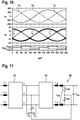
- Fig. 10 shows a diagram analogously to Fig. 8 . Contrary to Fig. 8 , a whole oscillation of the input voltages u a , u b , u c is depicted. In the lower part of Fig. 10 , it is indicated that the switches of the input voltage selector are not simply switched from on to off and vice versa during the corresponding crossing of the AC input voltages. They are switched on and off according to the control method as described above, thus the current distortions in the currents i a , i b , i c in the vicinity of the crossings are mitigated.
- Fig. 11 shows a further electrical converter 10, which may have an input voltage selector 12 and an output converter 14 as described above.
- the output converter 14 has a common mode filter 26 connected to its two DC outputs p, n.
- the common mode filter 26 comprises a common mode inductor L CM with a winding in each output p, n and a common core.
- the common mode filter 26 comprises two series connected common mode capacitors C CM1 , C CM2 , which are connecting the two outputs p, n.
- the point between the two capacitors C CM1 , C CM2 may be connected to the star-point of the capacitors C x , C y , C z interconnecting the nodes x, y, z between the input voltage selector 12 and the output converter 14.
Landscapes
- Engineering & Computer Science (AREA)
- Power Engineering (AREA)
- Rectifiers (AREA)
Claims (13)
- Convertisseur électrique (10), comprenant :un sélecteur de tension d'entrée (12) pour convertir une tension d'entrée alternative triphasée fournie sur trois entrées de phase (a, b, c) du convertisseur électrique en trois tensions intermédiaires fournies sur un nœud à tension supérieure (x), un nœud à tension médiane (y) et un nœud à tension inférieure (z) ;des condensateurs de filtrage (Cx, Cy, Cz) interconnectant le nœud à tension supérieure (x), le nœud à tension médiane (y) et le nœud à tension inférieure (z) ;un convertisseur de sortie (14) pour convertir les trois tensions intermédiaires en une tension de sortie ;dans lequel une inductance de filtrage (Lf) est interconnectée dans chaque entrée de phase (a, b, c) et des condensateurs de filtrage (Cx, Cy, Cz) sont disposés uniquement derrière le sélecteur de tension d'entrée du point de vue des entrées de phase (a, b, c) ;dans lequel le nœud à tension supérieure (x), le nœud à tension médiane (y) et le nœud à tension inférieure (z) sont connectés en étoile ou connectés en delta par l'intermédiaire des condensateurs de filtrage (Cx, Cy, Cz) ;dans lequel le convertisseur électrique comprend un dispositif de commande conçu pour faire commuter des commutateurs à semi-conducteurs du sélecteur de tension d'entrée (12) de telle sorte que le nœud à tension supérieure (x) soit connecté à l'entrée de phase (a, b, c) ayant la tension la plus élevée de la tension d'entrée alternative triphasée, que le nœud à tension inférieure (z) soit connecté à l'entrée de phase (a, b, c) ayant la tension la plus basse de la tension d'entrée de la tension alternative triphasée, et que le nœud à tension médiane (y) soit connecté à l'entrée de phase (a, b, c) ayant une tension comprise entre la tension la plus élevée et la tension la plus basse ;caractérisé en ce que,lorsque deux des tensions de la tension d'entrée alternative triphasée se croisent, le dispositif de commande est configuré pour faire commuter des commutateurs à semi-conducteurs du sélecteur de tension d'entrée (12) de telle sorte que les deux entrées de phase correspondantes (
a ,b ,c ) soient court-circuitées afin de réduire les distorsions de courant dans les entrées de phase (a, b, c) du convertisseur électrique (10) ;dans lequel les deux entrées de phase (a, b, c) du convertisseur électrique et les inductances de phase correspondantes sont court-circuitées de telle sorte qu'une moyenne de tension d'une tension entre les entrées de phase correspondantes (a ,b ,c ) du sélecteur de tension d'entrée (12) soit égale à une tension de réseau fournie entre les deux entrées de phase (a, b, c) du convertisseur électrique (10) ; etune durée, pendant laquelle les deux entrées de phase (a, b, c) sont court-circuitées, est déterminée de telle sorte que pendant chaque cycle de commutation d'une technique de modulation PWM du convertisseur de sortie, la moyenne de tension soit égale à une tension de réseau fournie entre les deux entrées de phase (a, b, c) du convertisseur électrique (10). - Convertisseur électrique (10) selon la revendication 1,
dans lequel chacun du nœud à tension supérieure (x), du nœud à tension médiane (y) et du nœud à tension inférieure (z) est connecté par l'intermédiaire d'une inductance de filtrage (Lf) aux condensateurs de filtrage (Cx, Cy, Cz) interconnectant le nœud à tension supérieure (x), le nœud à tension médiane (y) et le nœud à tension inférieure (z) . - Convertisseur électrique (10) selon la revendication 1 ou 2,
dans lequel le sélecteur de tension d'entrée (12) comprend trois branches de sélecteur (16) pour interconnecter l'une des entrées de phase (a, b, c) au nœud à tension supérieure (x), au nœud à tension médiane (y) et au nœud à tension inférieure (z), chaque branche de sélecteur (16) comprenant un demi-pont (18) et une unité de commutation d'injecteur (20), le demi-pont (18) étant connecté au nœud à tension supérieure (x) et au nœud à tension inférieure (z) et l'unité de commutation d'injecteur (20) étant connectée au nœud à tension médiane (z). - Convertisseur électrique (10) selon la revendication 3,
dans lequel le demi-pont (18) comprend des diodes. - Convertisseur électrique (10) selon la revendication 3 ou 4,
dans lequel le demi-pont (18) comprend des commutateurs à semi-conducteurs commandables. - Convertisseur électrique (10) selon l'une des revendications 3 à 5,dans lequel l'unité de commutation d'injecteur (20) comprend deux commutateurs à semi-conducteurs connectés en série, qui sont inversés l'un par rapport à l'autre ; oudans lequel l'unité de commutation d'injecteur (20) comprend un commutateur à semi-conducteur commandable interconnecté en parallèle avec deux paires de deux diodes connectées en série ; oudans lequel l'unité de commande d'injecteur (20) comprend un demi-pont de diodes et/ou de commutateurs à semi-conducteurs commandables.
- Convertisseur électrique (10) selon l'une des revendications 3 à 6,dans lequel l'unité de commutation d'injecteur (20) interconnecte un point médian du demi-pont (18) au nœud à tension médiane (y) ; oudans lequel l'unité de commutation d'injecteur (20) est interconnectée entre des bras du demi-pont (18).
- Convertisseur électrique (10) selon l'une des revendications précédentes,
dans lequel le convertisseur de sortie est ou comprend au moins l'un des éléments suivants :un convertisseur élévateur (14a),un convertisseur abaisseur-élévateur non-inverseur (14b),un convertisseur SEPIC (14c),un convertisseur Cuk (14d),un convertisseur abaisseur-élévateur inverseur (14e),des convertisseurs abaisseurs entrelacés (14f). - Convertisseur électrique (10) selon l'une des revendications précédentes,
dans lequel le convertisseur de sortie est un convertisseur continu-continu (14, 14a à 141) ou un convertisseur continu-alternatif (14m, 14n) ; et/ou dans lequel le convertisseur de sortie est un convertisseur de sortie isolé (14k, 141) comprenant un transformateur entre deux unités de sous-convertisseur. - Convertisseur électrique (10) selon l'une des revendications précédentes,
dans lequel le convertisseur de sortie (14g à 14j, 14m, 14n) comprend des demi-ponts à trois niveaux ; et/ou dans lequel les demi-ponts sont à base de NPC ou à base de type T. - Convertisseur électrique (10) selon l'une des revendications précédentes,dans lequel un filtre de mode commun (26) est prévu à une sortie (p, n) du convertisseur de sortie (14) ; et facultativementdans lequel un point d'étoile des condensateurs de filtrage (Cx, Cy, Cz) interconnectant le nœud à tension supérieure (x), le nœud à tension médiane (y) et le nœud à tension inférieure (z) est connecté au filtre de mode commun (26).
- Procédé de commande d'un convertisseur électrique (10) selon l'une des revendications précédentes, dans lequel le procédé est exécuté par le dispositif de commande du convertisseur électrique (10) et comprend :la commutation de commutateurs à semi-conducteurs du sélecteur de tension d'entrée (12) de telle sorte que le nœud à tension supérieure (x) soit connecté à l'entrée de phase (a, b, c) ayant la tension la plus élevée de la tension d'entrée alternative triphasée, que le nœud à tension inférieure (z) soit connecté à l'entrée de phase (a, b, c) ayant la tension la plus basse de la tension d'entrée alternative triphasée, et que le nœud à tension médiane (y) soit connecté à l'entrée de phase (a, b, c) ayant une tension comprise entre la tension la plus élevée et la tension la plus basse ;caractérisé en ce que,lorsque deux des tensions de la tension d'entrée alternative triphasée se croisent, les commutateurs à semi-conducteurs du sélecteur de tension d'entrée (12) sont commutés de telle sorte que les deux entrées de phase correspondantes (
a ,b ,c ) soient court-circuitées afin de réduire les distorsions de courant dans les entrées de phase (a, b, c) du convertisseur électrique (10) ;en ce que les deux entrées de phase (a, b, c) du convertisseur électrique et les inductances de phase correspondantes sont court-circuitées de telle sorte qu'une moyenne de tension d'une tension entre les entrées de phase correspondantes (a ,b ,c ) du sélecteur de tension d'entrée (12) soit égale à une tension de réseau fournie entre les deux entrées de phase (a, b, c) du convertisseur électrique (10) ; eten ce qu'une durée, pendant laquelle les deux entrées de phase (a, b, c) sont court-circuitées, est déterminée de telle sorte que pendant chaque cycle de commutation d'une technique de modulation PWM du convertisseur de sortie, la moyenne de tension soit égale à une tension de réseau fournie entre les deux entrées de phase (a, b, c) du convertisseur électrique (10). - Procédé selon la revendication 12,
dans lequel l'instant où les deux entrées de phase (a, b, c) sont court-circuitées est déterminé sur la base d'un instant où un commutateur à semi-conducteur du convertisseur électrique (10) est commuté sur la base d'une technique de modulation PWM.
Priority Applications (2)
| Application Number | Priority Date | Filing Date | Title |
|---|---|---|---|
| EP15174720.1A EP3113345B1 (fr) | 2015-07-01 | 2015-07-01 | Convertisseur électrique et procédé de commande |
| ES15174720T ES2908960T3 (es) | 2015-07-01 | 2015-07-01 | Convertidor eléctrico y método de control |
Applications Claiming Priority (1)
| Application Number | Priority Date | Filing Date | Title |
|---|---|---|---|
| EP15174720.1A EP3113345B1 (fr) | 2015-07-01 | 2015-07-01 | Convertisseur électrique et procédé de commande |
Publications (2)
| Publication Number | Publication Date |
|---|---|
| EP3113345A1 EP3113345A1 (fr) | 2017-01-04 |
| EP3113345B1 true EP3113345B1 (fr) | 2022-02-23 |
Family
ID=53510696
Family Applications (1)
| Application Number | Title | Priority Date | Filing Date |
|---|---|---|---|
| EP15174720.1A Active EP3113345B1 (fr) | 2015-07-01 | 2015-07-01 | Convertisseur électrique et procédé de commande |
Country Status (2)
| Country | Link |
|---|---|
| EP (1) | EP3113345B1 (fr) |
| ES (1) | ES2908960T3 (fr) |
Families Citing this family (17)
| Publication number | Priority date | Publication date | Assignee | Title |
|---|---|---|---|---|
| WO2018126393A1 (fr) | 2017-01-05 | 2018-07-12 | General Electric Company | Station de recharge rapide c.c. pour véhicules électriques |
| US10326357B1 (en) * | 2018-07-31 | 2019-06-18 | Raytheon Company | Adaptive power converter topologies supporting active power factor correction (PFC) |
| NL2021926B1 (en) * | 2018-11-02 | 2020-05-14 | Prodrive Tech Bv | Electrical power converter |
| DE102019102550B4 (de) * | 2019-02-01 | 2022-06-30 | Infineon Technologies Austria Ag | Leistungswandler und leistungswandlungsverfahren |
| US10917019B2 (en) | 2019-03-11 | 2021-02-09 | Utah State University | Quasi-single stage power converter topology |
| WO2020221807A1 (fr) * | 2019-05-02 | 2020-11-05 | Prodrive Technologies B.V. | Convertisseur électrique |
| CN112838773A (zh) | 2019-11-25 | 2021-05-25 | 开利公司 | 具有不对称半导体额定值布置的功率模块和转换器 |
| CN111431394B (zh) * | 2020-04-17 | 2024-08-02 | 广东工业大学 | 一种降压式单相三电平无桥pfc变换器系统的控制方法 |
| NL2025502B1 (en) * | 2020-05-04 | 2021-11-18 | Prodrive Tech Bv | Electrical power converter with pre-charge mode of operation |
| CN112532038B (zh) * | 2020-10-27 | 2021-12-28 | 东南大学 | 降低三相史维斯电路边界处电流畸变的控制系统及方法 |
| DE102020214265A1 (de) * | 2020-11-12 | 2022-05-12 | Universität Paderborn | Vorrichtung zur gleichtaktarmen Umrichtung von Wechselspannung |
| DE102021206982A1 (de) * | 2021-07-02 | 2023-01-05 | Universität Paderborn, Körperschaft des öffentlichen Rechts | Transformatorloses On-Board -Ladegerät für Elektrofahrzeuge und Verfahren zur Ansteuerung einer DC/DC-Stufe in einem transformatorlosen On-Board-Ladegerät für Elektrofahrzeuge |
| CN113783453B (zh) * | 2021-09-29 | 2023-07-07 | 山东建筑大学 | 一种低成本高增益三电平逆变器及其空间矢量调制方法 |
| TR2022008988A1 (tr) * | 2022-06-01 | 2023-12-21 | Aselsan Elektroni̇k Sanayi̇ Ve Ti̇caret Anoni̇m Şi̇rketi̇ | Üç fazli, üç sevi̇yeli̇, trafosuz, düşüren-yükselten evi̇ri̇ci̇ |
| CN115102417B (zh) * | 2022-06-06 | 2024-01-12 | 江苏科曜能源科技有限公司 | 一种四线三电平储能变换器 |
| CN116365890B (zh) * | 2023-05-04 | 2023-11-24 | 西南交通大学 | 一种三相交错t型三电平llc变换器及其宽变压控制方法 |
| DE102023211916B4 (de) * | 2023-11-29 | 2025-07-31 | Zf Friedrichshafen Ag | Ladeschaltung für ein elektrisch antreibbares Kraftfahrzeug |
Family Cites Families (3)
| Publication number | Priority date | Publication date | Assignee | Title |
|---|---|---|---|---|
| US20090040800A1 (en) * | 2007-08-10 | 2009-02-12 | Maximiliano Sonnaillon | Three phase rectifier and rectification method |
| CH704553B1 (de) * | 2011-02-21 | 2016-06-15 | Eth Zürich Eth Transfer | Hybrider dreiphasiger AC/DC-Konverter und Verfahren zu dessen Steuerung. |
| AT514654B1 (de) * | 2013-08-13 | 2019-05-15 | Schneider Electric Power Drives Gmbh | Gleichrichterschaltung mit Strominjektion |
-
2015
- 2015-07-01 EP EP15174720.1A patent/EP3113345B1/fr active Active
- 2015-07-01 ES ES15174720T patent/ES2908960T3/es active Active
Also Published As
| Publication number | Publication date |
|---|---|
| EP3113345A1 (fr) | 2017-01-04 |
| ES2908960T3 (es) | 2022-05-04 |
Similar Documents
| Publication | Publication Date | Title |
|---|---|---|
| EP3113345B1 (fr) | Convertisseur électrique et procédé de commande | |
| Sahoo et al. | A three-level LC-switching-based voltage boost NPC inverter | |
| US10978948B2 (en) | Interleaved multi-channel, multi-level, multi-quadrant DC-DC converters | |
| Khan et al. | An improved single-phase direct PWM inverting buck–boost AC–AC converter | |
| Ahmed et al. | A novel buck–boost AC–AC converter with both inverting and noninverting operations and without commutation problem | |
| EP3956972B1 (fr) | Convertisseur électrique | |
| JP7309870B2 (ja) | 電力変換器 | |
| Siwakoti et al. | Power electronics converters—An overview | |
| JP5687498B2 (ja) | 電力変換システム | |
| JP2013504295A (ja) | 電気エネルギ変換回路装置 | |
| US11065968B2 (en) | Integrated multi-source IPT system | |
| US12040713B2 (en) | DC-DC converter of power conversion system | |
| Valipour et al. | Extended range bridgeless PFC converter with high-voltage DC bus and small inductor | |
| Yuan | A four-level π-type converter for low-voltage applications | |
| US20150003132A1 (en) | Inverter with less snubber capacitors | |
| Barbie et al. | Modeling and simulation of a novel active three-phase multilevel power factor correction front end–The “Negev” rectifier | |
| Tan et al. | A bipolar-DC-bus EV fast charging station with intrinsic DC-bus voltages equalization and minimized voltage ripples | |
| Kang et al. | Optimized coupling factor design of multiple-phase coupled inductor for minimum inductor current ripple operation in EV charger systems | |
| Li et al. | A boost-Full-Bridge-type single-Active-bridge isolated AC-DC converter | |
| CN114008902A (zh) | 电转换器 | |
| Nayak et al. | An asymmetrical space vector PWM scheme for a three phase single-stage DC-AC Converter | |
| Karaman et al. | A 3Ф-3Ф quasi Z-source matrix converter for residential wind energy systems | |
| Gaafar et al. | Multi‐input transformer‐less four‐wire microinverter with distributed MPPT for PV systems | |
| Rizet et al. | A simplified resonant pole for three-level soft-switching PFC rectifier used in UPS | |
| US20240333124A1 (en) | Balancer Circuit for Series Connection of Two DC-Link Capacitors, Method for Controlling the Balancer Circuit and Converter Arrangement |
Legal Events
| Date | Code | Title | Description |
|---|---|---|---|
| PUAI | Public reference made under article 153(3) epc to a published international application that has entered the european phase |
Free format text: ORIGINAL CODE: 0009012 |
|
| STAA | Information on the status of an ep patent application or granted ep patent |
Free format text: STATUS: THE APPLICATION HAS BEEN PUBLISHED |
|
| AK | Designated contracting states |
Kind code of ref document: A1 Designated state(s): AL AT BE BG CH CY CZ DE DK EE ES FI FR GB GR HR HU IE IS IT LI LT LU LV MC MK MT NL NO PL PT RO RS SE SI SK SM TR |
|
| AX | Request for extension of the european patent |
Extension state: BA ME |
|
| RAP1 | Party data changed (applicant data changed or rights of an application transferred) |
Owner name: ABB SCHWEIZ AG |
|
| STAA | Information on the status of an ep patent application or granted ep patent |
Free format text: STATUS: REQUEST FOR EXAMINATION WAS MADE |
|
| 17P | Request for examination filed |
Effective date: 20170703 |
|
| RBV | Designated contracting states (corrected) |
Designated state(s): AL AT BE BG CH CY CZ DE DK EE ES FI FR GB GR HR HU IE IS IT LI LT LU LV MC MK MT NL NO PL PT RO RS SE SI SK SM TR |
|
| STAA | Information on the status of an ep patent application or granted ep patent |
Free format text: STATUS: EXAMINATION IS IN PROGRESS |
|
| 17Q | First examination report despatched |
Effective date: 20181022 |
|
| GRAP | Despatch of communication of intention to grant a patent |
Free format text: ORIGINAL CODE: EPIDOSNIGR1 |
|
| STAA | Information on the status of an ep patent application or granted ep patent |
Free format text: STATUS: GRANT OF PATENT IS INTENDED |
|
| RIC1 | Information provided on ipc code assigned before grant |
Ipc: H02M 1/00 20060101ALN20210902BHEP Ipc: H02M 7/487 20070101ALN20210902BHEP Ipc: H02M 7/483 20070101ALN20210902BHEP Ipc: H02M 3/335 20060101ALN20210902BHEP Ipc: H02M 3/00 20060101ALN20210902BHEP Ipc: H02M 3/155 20060101ALN20210902BHEP Ipc: H02M 7/217 20060101ALI20210902BHEP Ipc: H02M 7/06 20060101ALI20210902BHEP Ipc: H02M 3/158 20060101ALI20210902BHEP Ipc: H02M 1/42 20070101ALI20210902BHEP Ipc: H02M 1/12 20060101AFI20210902BHEP |
|
| INTG | Intention to grant announced |
Effective date: 20210923 |
|
| RAP3 | Party data changed (applicant data changed or rights of an application transferred) |
Owner name: ABB SCHWEIZ AG |
|
| GRAS | Grant fee paid |
Free format text: ORIGINAL CODE: EPIDOSNIGR3 |
|
| GRAA | (expected) grant |
Free format text: ORIGINAL CODE: 0009210 |
|
| STAA | Information on the status of an ep patent application or granted ep patent |
Free format text: STATUS: THE PATENT HAS BEEN GRANTED |
|
| AK | Designated contracting states |
Kind code of ref document: B1 Designated state(s): AL AT BE BG CH CY CZ DE DK EE ES FI FR GB GR HR HU IE IS IT LI LT LU LV MC MK MT NL NO PL PT RO RS SE SI SK SM TR |
|
| REG | Reference to a national code |
Ref country code: GB Ref legal event code: FG4D |
|
| REG | Reference to a national code |
Ref country code: CH Ref legal event code: EP |
|
| REG | Reference to a national code |
Ref country code: DE Ref legal event code: R096 Ref document number: 602015077040 Country of ref document: DE |
|
| REG | Reference to a national code |
Ref country code: AT Ref legal event code: REF Ref document number: 1471212 Country of ref document: AT Kind code of ref document: T Effective date: 20220315 |
|
| REG | Reference to a national code |
Ref country code: IE Ref legal event code: FG4D |
|
| REG | Reference to a national code |
Ref country code: ES Ref legal event code: FG2A Ref document number: 2908960 Country of ref document: ES Kind code of ref document: T3 Effective date: 20220504 |
|
| REG | Reference to a national code |
Ref country code: LT Ref legal event code: MG9D |
|
| REG | Reference to a national code |
Ref country code: NL Ref legal event code: MP Effective date: 20220223 |
|
| REG | Reference to a national code |
Ref country code: AT Ref legal event code: MK05 Ref document number: 1471212 Country of ref document: AT Kind code of ref document: T Effective date: 20220223 |
|
| PG25 | Lapsed in a contracting state [announced via postgrant information from national office to epo] |
Ref country code: SE Free format text: LAPSE BECAUSE OF FAILURE TO SUBMIT A TRANSLATION OF THE DESCRIPTION OR TO PAY THE FEE WITHIN THE PRESCRIBED TIME-LIMIT Effective date: 20220223 Ref country code: RS Free format text: LAPSE BECAUSE OF FAILURE TO SUBMIT A TRANSLATION OF THE DESCRIPTION OR TO PAY THE FEE WITHIN THE PRESCRIBED TIME-LIMIT Effective date: 20220223 Ref country code: PT Free format text: LAPSE BECAUSE OF FAILURE TO SUBMIT A TRANSLATION OF THE DESCRIPTION OR TO PAY THE FEE WITHIN THE PRESCRIBED TIME-LIMIT Effective date: 20220623 Ref country code: NO Free format text: LAPSE BECAUSE OF FAILURE TO SUBMIT A TRANSLATION OF THE DESCRIPTION OR TO PAY THE FEE WITHIN THE PRESCRIBED TIME-LIMIT Effective date: 20220523 Ref country code: NL Free format text: LAPSE BECAUSE OF FAILURE TO SUBMIT A TRANSLATION OF THE DESCRIPTION OR TO PAY THE FEE WITHIN THE PRESCRIBED TIME-LIMIT Effective date: 20220223 Ref country code: LT Free format text: LAPSE BECAUSE OF FAILURE TO SUBMIT A TRANSLATION OF THE DESCRIPTION OR TO PAY THE FEE WITHIN THE PRESCRIBED TIME-LIMIT Effective date: 20220223 Ref country code: HR Free format text: LAPSE BECAUSE OF FAILURE TO SUBMIT A TRANSLATION OF THE DESCRIPTION OR TO PAY THE FEE WITHIN THE PRESCRIBED TIME-LIMIT Effective date: 20220223 Ref country code: BG Free format text: LAPSE BECAUSE OF FAILURE TO SUBMIT A TRANSLATION OF THE DESCRIPTION OR TO PAY THE FEE WITHIN THE PRESCRIBED TIME-LIMIT Effective date: 20220523 |
|
| PG25 | Lapsed in a contracting state [announced via postgrant information from national office to epo] |
Ref country code: PL Free format text: LAPSE BECAUSE OF FAILURE TO SUBMIT A TRANSLATION OF THE DESCRIPTION OR TO PAY THE FEE WITHIN THE PRESCRIBED TIME-LIMIT Effective date: 20220223 Ref country code: LV Free format text: LAPSE BECAUSE OF FAILURE TO SUBMIT A TRANSLATION OF THE DESCRIPTION OR TO PAY THE FEE WITHIN THE PRESCRIBED TIME-LIMIT Effective date: 20220223 Ref country code: GR Free format text: LAPSE BECAUSE OF FAILURE TO SUBMIT A TRANSLATION OF THE DESCRIPTION OR TO PAY THE FEE WITHIN THE PRESCRIBED TIME-LIMIT Effective date: 20220524 Ref country code: FI Free format text: LAPSE BECAUSE OF FAILURE TO SUBMIT A TRANSLATION OF THE DESCRIPTION OR TO PAY THE FEE WITHIN THE PRESCRIBED TIME-LIMIT Effective date: 20220223 Ref country code: AT Free format text: LAPSE BECAUSE OF FAILURE TO SUBMIT A TRANSLATION OF THE DESCRIPTION OR TO PAY THE FEE WITHIN THE PRESCRIBED TIME-LIMIT Effective date: 20220223 |
|
| PG25 | Lapsed in a contracting state [announced via postgrant information from national office to epo] |
Ref country code: IS Free format text: LAPSE BECAUSE OF FAILURE TO SUBMIT A TRANSLATION OF THE DESCRIPTION OR TO PAY THE FEE WITHIN THE PRESCRIBED TIME-LIMIT Effective date: 20220623 |
|
| PG25 | Lapsed in a contracting state [announced via postgrant information from national office to epo] |
Ref country code: SM Free format text: LAPSE BECAUSE OF FAILURE TO SUBMIT A TRANSLATION OF THE DESCRIPTION OR TO PAY THE FEE WITHIN THE PRESCRIBED TIME-LIMIT Effective date: 20220223 Ref country code: SK Free format text: LAPSE BECAUSE OF FAILURE TO SUBMIT A TRANSLATION OF THE DESCRIPTION OR TO PAY THE FEE WITHIN THE PRESCRIBED TIME-LIMIT Effective date: 20220223 Ref country code: RO Free format text: LAPSE BECAUSE OF FAILURE TO SUBMIT A TRANSLATION OF THE DESCRIPTION OR TO PAY THE FEE WITHIN THE PRESCRIBED TIME-LIMIT Effective date: 20220223 Ref country code: EE Free format text: LAPSE BECAUSE OF FAILURE TO SUBMIT A TRANSLATION OF THE DESCRIPTION OR TO PAY THE FEE WITHIN THE PRESCRIBED TIME-LIMIT Effective date: 20220223 Ref country code: DK Free format text: LAPSE BECAUSE OF FAILURE TO SUBMIT A TRANSLATION OF THE DESCRIPTION OR TO PAY THE FEE WITHIN THE PRESCRIBED TIME-LIMIT Effective date: 20220223 Ref country code: CZ Free format text: LAPSE BECAUSE OF FAILURE TO SUBMIT A TRANSLATION OF THE DESCRIPTION OR TO PAY THE FEE WITHIN THE PRESCRIBED TIME-LIMIT Effective date: 20220223 |
|
| REG | Reference to a national code |
Ref country code: DE Ref legal event code: R097 Ref document number: 602015077040 Country of ref document: DE |
|
| PG25 | Lapsed in a contracting state [announced via postgrant information from national office to epo] |
Ref country code: AL Free format text: LAPSE BECAUSE OF FAILURE TO SUBMIT A TRANSLATION OF THE DESCRIPTION OR TO PAY THE FEE WITHIN THE PRESCRIBED TIME-LIMIT Effective date: 20220223 |
|
| PLBE | No opposition filed within time limit |
Free format text: ORIGINAL CODE: 0009261 |
|
| STAA | Information on the status of an ep patent application or granted ep patent |
Free format text: STATUS: NO OPPOSITION FILED WITHIN TIME LIMIT |
|
| 26N | No opposition filed |
Effective date: 20221124 |
|
| PG25 | Lapsed in a contracting state [announced via postgrant information from national office to epo] |
Ref country code: SI Free format text: LAPSE BECAUSE OF FAILURE TO SUBMIT A TRANSLATION OF THE DESCRIPTION OR TO PAY THE FEE WITHIN THE PRESCRIBED TIME-LIMIT Effective date: 20220223 Ref country code: MC Free format text: LAPSE BECAUSE OF FAILURE TO SUBMIT A TRANSLATION OF THE DESCRIPTION OR TO PAY THE FEE WITHIN THE PRESCRIBED TIME-LIMIT Effective date: 20220223 |
|
| REG | Reference to a national code |
Ref country code: BE Ref legal event code: MM Effective date: 20220731 |
|
| PG25 | Lapsed in a contracting state [announced via postgrant information from national office to epo] |
Ref country code: LU Free format text: LAPSE BECAUSE OF NON-PAYMENT OF DUE FEES Effective date: 20220701 |
|
| PG25 | Lapsed in a contracting state [announced via postgrant information from national office to epo] |
Ref country code: BE Free format text: LAPSE BECAUSE OF NON-PAYMENT OF DUE FEES Effective date: 20220731 |
|
| PG25 | Lapsed in a contracting state [announced via postgrant information from national office to epo] |
Ref country code: IE Free format text: LAPSE BECAUSE OF NON-PAYMENT OF DUE FEES Effective date: 20220701 |
|
| PG25 | Lapsed in a contracting state [announced via postgrant information from national office to epo] |
Ref country code: HU Free format text: LAPSE BECAUSE OF FAILURE TO SUBMIT A TRANSLATION OF THE DESCRIPTION OR TO PAY THE FEE WITHIN THE PRESCRIBED TIME-LIMIT; INVALID AB INITIO Effective date: 20150701 |
|
| PG25 | Lapsed in a contracting state [announced via postgrant information from national office to epo] |
Ref country code: MK Free format text: LAPSE BECAUSE OF FAILURE TO SUBMIT A TRANSLATION OF THE DESCRIPTION OR TO PAY THE FEE WITHIN THE PRESCRIBED TIME-LIMIT Effective date: 20220223 Ref country code: CY Free format text: LAPSE BECAUSE OF FAILURE TO SUBMIT A TRANSLATION OF THE DESCRIPTION OR TO PAY THE FEE WITHIN THE PRESCRIBED TIME-LIMIT Effective date: 20220223 |
|
| PG25 | Lapsed in a contracting state [announced via postgrant information from national office to epo] |
Ref country code: MT Free format text: LAPSE BECAUSE OF FAILURE TO SUBMIT A TRANSLATION OF THE DESCRIPTION OR TO PAY THE FEE WITHIN THE PRESCRIBED TIME-LIMIT Effective date: 20220223 |
|
| PGFP | Annual fee paid to national office [announced via postgrant information from national office to epo] |
Ref country code: ES Payment date: 20250826 Year of fee payment: 11 |
|
| PGFP | Annual fee paid to national office [announced via postgrant information from national office to epo] |
Ref country code: DE Payment date: 20250722 Year of fee payment: 11 |
|
| PGFP | Annual fee paid to national office [announced via postgrant information from national office to epo] |
Ref country code: IT Payment date: 20250724 Year of fee payment: 11 |
|
| PGFP | Annual fee paid to national office [announced via postgrant information from national office to epo] |
Ref country code: GB Payment date: 20250722 Year of fee payment: 11 |
|
| PGFP | Annual fee paid to national office [announced via postgrant information from national office to epo] |
Ref country code: FR Payment date: 20250725 Year of fee payment: 11 |
|
| PGFP | Annual fee paid to national office [announced via postgrant information from national office to epo] |
Ref country code: CH Payment date: 20250801 Year of fee payment: 11 |
|
| PG25 | Lapsed in a contracting state [announced via postgrant information from national office to epo] |
Ref country code: TR Free format text: LAPSE BECAUSE OF FAILURE TO SUBMIT A TRANSLATION OF THE DESCRIPTION OR TO PAY THE FEE WITHIN THE PRESCRIBED TIME-LIMIT Effective date: 20220223 |