EP3116128A2 - Pegelschieber und ansatz dafür - Google Patents
Pegelschieber und ansatz dafür Download PDFInfo
- Publication number
- EP3116128A2 EP3116128A2 EP16175288.6A EP16175288A EP3116128A2 EP 3116128 A2 EP3116128 A2 EP 3116128A2 EP 16175288 A EP16175288 A EP 16175288A EP 3116128 A2 EP3116128 A2 EP 3116128A2
- Authority
- EP
- European Patent Office
- Prior art keywords
- circuit
- voltage level
- output
- voltage
- driver circuit
- Prior art date
- Legal status (The legal status is an assumption and is not a legal conclusion. Google has not performed a legal analysis and makes no representation as to the accuracy of the status listed.)
- Withdrawn
Links
- 238000013459 approach Methods 0.000 title description 16
- 230000004044 response Effects 0.000 claims abstract description 26
- 230000007704 transition Effects 0.000 claims abstract description 19
- 230000008878 coupling Effects 0.000 claims description 7
- 238000010168 coupling process Methods 0.000 claims description 7
- 238000005859 coupling reaction Methods 0.000 claims description 7
- 238000000034 method Methods 0.000 claims description 5
- 102100036285 25-hydroxyvitamin D-1 alpha hydroxylase, mitochondrial Human genes 0.000 description 14
- 101000875403 Homo sapiens 25-hydroxyvitamin D-1 alpha hydroxylase, mitochondrial Proteins 0.000 description 14
- 101100489717 Saccharomyces cerevisiae (strain ATCC 204508 / S288c) GND2 gene Proteins 0.000 description 11
- 238000002955 isolation Methods 0.000 description 10
- 101100489713 Saccharomyces cerevisiae (strain ATCC 204508 / S288c) GND1 gene Proteins 0.000 description 9
- 238000001514 detection method Methods 0.000 description 9
- 239000003990 capacitor Substances 0.000 description 5
- 238000012986 modification Methods 0.000 description 4
- 230000004048 modification Effects 0.000 description 4
- 230000000694 effects Effects 0.000 description 3
- 239000000872 buffer Substances 0.000 description 2
- 238000006243 chemical reaction Methods 0.000 description 2
- 230000001419 dependent effect Effects 0.000 description 2
- 230000003068 static effect Effects 0.000 description 2
- 238000013519 translation Methods 0.000 description 2
- 230000009471 action Effects 0.000 description 1
- 230000009286 beneficial effect Effects 0.000 description 1
- 230000008901 benefit Effects 0.000 description 1
- 230000000295 complement effect Effects 0.000 description 1
- 230000003247 decreasing effect Effects 0.000 description 1
- 230000003028 elevating effect Effects 0.000 description 1
- 230000008569 process Effects 0.000 description 1
- 238000004064 recycling Methods 0.000 description 1
- 230000009467 reduction Effects 0.000 description 1
Images





Classifications
-
- H—ELECTRICITY
- H03—ELECTRONIC CIRCUITRY
- H03K—PULSE TECHNIQUE
- H03K19/00—Logic circuits, i.e. having at least two inputs acting on one output; Inverting circuits
- H03K19/0175—Coupling arrangements; Interface arrangements
- H03K19/017509—Interface arrangements
-
- H—ELECTRICITY
- H03—ELECTRONIC CIRCUITRY
- H03K—PULSE TECHNIQUE
- H03K19/00—Logic circuits, i.e. having at least two inputs acting on one output; Inverting circuits
- H03K19/0175—Coupling arrangements; Interface arrangements
- H03K19/0185—Coupling arrangements; Interface arrangements using field effect transistors only
- H03K19/018507—Interface arrangements
- H03K19/018514—Interface arrangements with at least one differential stage
-
- H—ELECTRICITY
- H03—ELECTRONIC CIRCUITRY
- H03K—PULSE TECHNIQUE
- H03K3/00—Circuits for generating electric pulses; Monostable, bistable or multistable circuits
- H03K3/02—Generators characterised by the type of circuit or by the means used for producing pulses
- H03K3/353—Generators characterised by the type of circuit or by the means used for producing pulses by the use, as active elements, of field-effect transistors with internal or external positive feedback
- H03K3/356—Bistable circuits
- H03K3/356104—Bistable circuits using complementary field-effect transistors
- H03K3/356182—Bistable circuits using complementary field-effect transistors with additional means for controlling the main nodes
-
- H—ELECTRICITY
- H03—ELECTRONIC CIRCUITRY
- H03K—PULSE TECHNIQUE
- H03K19/00—Logic circuits, i.e. having at least two inputs acting on one output; Inverting circuits
- H03K19/0175—Coupling arrangements; Interface arrangements
- H03K19/0185—Coupling arrangements; Interface arrangements using field effect transistors only
-
- H—ELECTRICITY
- H03—ELECTRONIC CIRCUITRY
- H03K—PULSE TECHNIQUE
- H03K5/00—Manipulating of pulses not covered by one of the other main groups of this subclass
- H03K5/13—Arrangements having a single output and transforming input signals into pulses delivered at desired time intervals
Definitions
- aspects of various embodiments are directed to level shifting circuitry, which can be implemented for a variety of applications.
- Level shifters are implemented in a variety of manners, for various types of circuitry. For instance, level shifters may be used for interfacing between voltage stacks in which different types of circuitry operate under different voltage ranges (e.g. , between voltage rails at different voltage levels). In this context, level shifters may operate to receive an input signal from one power domain operating on one power level, shift the voltage level of the input signal, and pass the input signal having its voltage level shifted on to another power domain.
- level shifting circuits are susceptible to undesirable drawbacks. For instance, capacitors used in effecting various level shifting approaches may need to be relatively large, possibly forty times the size of other devices in the circuitry.
- level shifters can be susceptible to undesirable operation if there is a ripple in supply voltage or uneven supply voltage values for the two domains ( e.g. , capacitors may become inefficient).
- various level shifters can be functionally dependent upon an AC-path, which can render such level shifters prone to issues relating to signal frequency and slope (slew rate).
- an apparatus includes a first circuit that provides differential outputs that vary between first and second voltage levels, based on transitions of an input signal received from a first power domain that operates between the first and second voltage levels.
- a second circuit has first and second driver circuits coupled to a voltage rail that operates at the second voltage level, with the first driver circuit being coupled to a first one of the differential outputs and the second driver circuit being coupled to a second one of the differential outputs.
- a third driver circuit is coupled to a voltage rail that operates at a third voltage level in which the second voltage level is between the first and third voltage levels.
- the third driver circuit is configured and arranged with the first and second circuits to level-shift the input signal from the first power domain to an output signal on a second power domain that operates between the second and third voltage levels by driving an output circuit at the second voltage level in response to the input signal being at the first voltage level, and driving the output circuit at the third voltage level in response to the input signal being at the second voltage level.
- the apparatus operates to provide shifted operation in which the level of signals passed between circuit domains is shifted as above, and flat operation in which the level of signals passed between circuit domains is not shifted.
- Another embodiment is directed to a method as follows. Differential outputs are provided, which vary between first and second voltage levels based on transitions of an input signal received from a first power domain that operates between the first and second voltage levels.
- the input signal is level-shifted from the first power domain to an output signal on a second power domain that operates between the second and third voltage levels, using a first and second driver circuits coupled to a first voltage rail that operates at the second voltage level, in which the first driver circuit is coupled to a first one of the differential outputs and the second driver circuit is coupled to a second one of the differential outputs, and using a third driver circuit coupled to a second voltage rail that operates at a third voltage level in which the second voltage level is between the first and third voltage levels.
- the level shifting is carried out by driving an output circuit at the second voltage level in response to the input signal being at the first voltage level, and driving the output circuit at the third voltage level in response to the input signal being at the second voltage level.
- Another embodiment is directed to an apparatus having a level shifter circuit that passes communications between a first circuit that operates under a first power domain having a first voltage range, and a second circuit that operates under a second power domain having a second voltage range.
- the level shifter circuit passes communications directly between the first and second circuits in a flat mode in which the first and second voltage ranges are common, and level-shifts a voltage level of communications passed between the first and second circuits in a stacked mode in which the first and second voltage ranges are different.
- the level shifting is effected by providing differential outputs that vary between first and second voltage levels, based on transitions of an input signal received from a first power domain that operates between the first and second voltage levels.
- the input signal is level-shifted from the first power domain to an output signal on a second power domain that operates between second and third voltage levels by driving an output circuit at the second voltage level in response to the input signal being at the first voltage level, and driving the output circuit at the third voltage level in response to the input signal being at the second voltage level.
- the level shifter circuit includes first and second driver circuits coupled to a voltage rail that operates at the second voltage level, the first driver circuit being coupled to receive a first one of the differential outputs and the second driver circuit being coupled to receive a second one of the differential outputs.
- a third driver circuit is coupled to a voltage rail that operates at a third voltage level, in which the second voltage level is between the first and third voltage levels. The driver circuits drive the output circuit at the second and third voltage levels.
- aspects of the present disclosure are believed to be applicable to a variety of different types of apparatuses, systems and methods involving level shifting.
- aspects of the present disclosure have been shown to be beneficial when used in the context of communicating signals between respective power domains.
- a voltage level of such signals is shifted in applications for which high changes in voltage levels are implemented for communicating signals between stacked power domains.
- operating modes are effected such that an interface circuit operating to level shift selectively operates to directly pass signals for which level shifting is not necessary, facilitating desirable operational characteristics (e.g. , related to power loss).
- level shifting circuitry can be implemented in a manner that involves transistor-based level shifting that can be implemented without necessarily employing capacitors.
- a signal elevating up- and down- level shifter circuit is implemented with thin-oxide devices for stacked power domains.
- This approach can be implemented without a capacitor, can be manufactured with CMOS processes and can be integrated in standard cell rows.
- Such a circuit can be implemented with low leakage to support standby operation, using a main latch supported by two sub-latches.
- a first circuit provides differential outputs that vary between first and second voltage levels, based on transitions of an input signal received from a first power domain that operates between the first and second voltage levels.
- series inverters may be used to provide respective outputs.
- First and second drivers are respectively coupled to first and second ones of the differential outputs, and operate using a second voltage level.
- a third driver circuit operates using a third voltage level that is between the first and third voltage levels. The driver circuits level-shift the input signal from the first power domain to an output signal on a second power domain (e.g.
- the output signal is transitioned from the second voltage level to the third voltage level by switching the third driver circuit from a first state in which the third voltage level is provided to the output circuit, to a second state in which a voltage rail at the third voltage level is decoupled from the output circuit.
- the output signal is transitioned from the third voltage level to the second voltage level by switching the third driver circuit from the second state to the first state in which the third voltage level is provided to the output circuit.
- the third driver circuit may include, for example, first and second transistors as follows.
- the first transistor has its gate connected to an output of the second driver circuit and its source and drain connected between the voltage rail at the third voltage level and the output circuit.
- the second transistor has its gate connected to an output of the first driver circuit and the output circuit, and its source and drain connected between the second driver circuit and the voltage rail at the third voltage level.
- the first driver circuit includes third and fourth transistors, the third transistor having its gate driven by a first one of the differential outputs and having its source and drain coupled between the second voltage level and the output terminal.
- the fourth transistor has its gate driven by the second voltage level and its source and drain coupled between the first differential output and the output circuit.
- the second driver circuit includes fifth and sixth transistors, the fifth transistor having its gate driven by a second one of the differential outputs and its source and drain coupled between the second voltage level and the third driver circuit.
- the sixth transistor has its gate driven by the second voltage level and its source and drain coupled between the second differential output and the third driver circuit.
- the first circuit may include, for example, first and second inverter circuits that respectively invert the input signal and invert an output of the first inverter circuit.
- a seventh transistor has its source and drain coupled between the output of the first inverter circuit and the first driver circuit, and its gate connected to a voltage rail at the second voltage level.
- An eighth transistor has its source and drain coupled between an output of the second inverter circuit and the second driver circuit.
- the output circuit may further include an inverter having an input coupled to the first driver circuit and the third driver circuit.
- the output signal is generated by generating an output at the second voltage level in response to the input receiving the third voltage level, and generating an output at the third voltage level in response to the input receiving the second voltage level.
- a first one of a differential output as noted above is coupled to the first driver circuit while a second one of the differential outputs is decoupled from the second driver circuit for providing a first state of the input signal.
- a second state of the input signal is provided by coupling the second differential output to the second driver circuit and decoupling the first differential output from the first driver circuit.
- Another embodiment is directed to a method as follows. Differential outputs are provided, which vary between first and second voltage levels based on transitions of an input signal received from a first power domain that operates between the first and second voltage levels.
- the input signal is level-shifted from the first power domain to an output signal on a second power domain that operates between the second and third voltage levels, using first and second driver circuits coupled to a first voltage rail that operates at the second voltage level, in which the first driver circuit is coupled to a first one of the differential outputs and the second driver circuit is coupled to a second one of the differential outputs, and using a third driver circuit coupled to a second voltage rail that operate at a third voltage level in which the second voltage level is between the first and third voltage levels.
- the level shifting is carried out by driving an output circuit at the second voltage level in response to the input signal being at the first voltage level, and driving the output circuit at the third voltage level in response to the input signal being at the second voltage level.
- Such an approach may be implemented for addressing one or more issues as noted above (e.g. , without using a capacitive circuit to couple the first and second power domain).
- a first one of the differential outputs to the first driver circuit and a second one of the differential outputs is decoupled from the second driver circuit for a first state. In a second state, the second differential output is coupled to the second driver circuit, and the first differential output is decoupled from the first driver circuit.
- the output circuit is driven at the second and third voltage levels by operating the output circuit for a stacked operation in which signals are provided between respective power domains operating at different voltage ranges. A disabled mode is provided in flat operation by providing signals between respective power domains operating over a common voltage range.
- the output signal is driven from the second voltage level to the third voltage level by switching the third driver circuit from a first state in which the third voltage level is provided to the output circuit, to a second state in which a voltage rail at the third voltage level is decoupled from the output circuit.
- the output signal is transitioned from the third voltage level to the second voltage level by switching the third driver circuit from the second state to the first state in which the third voltage level is provided to the output circuit.
- the output circuit is driven at the second voltage level in response to the input receiving the first voltage level, and driven at the third voltage level in response to the input receiving the second voltage level.
- level shifters that include a transmitter, channel and receiver circuits.
- the transmitter handles signals coming from an input power domain, the channel interfaces between the input power domain and the output power domain, and the receiver provides signals to the output power domain.
- the transmitter may buffer the input signal and send it through the channel ( e.g., as implemented with a chain of inverters).
- the channel may include a DC (direct current) path and an AC (alternating current) path.
- the DC path which includes an inverter having its ground and power ports acting as an input and output, performs level translation of the input signal and provides the level-translated signal to the receiver side. This separates the two power domains and avoids overvoltage over what can be implemented as thin-oxide transistors in the transmitter and receiver.
- the AC path may address slow or power-consuming aspects of the DC path, and may include a large capacitor that couples the transmitter with the receiver and that ensures quick resolution or short meta-stability (thus decreasing delay and reducing power).
- the receiver such as a latch or other bi-stable circuit, regenerates level-translated voltage values from the channel to provide a digitally valid output.
- delay and the power consumption of the level shifter is dependent on the latch, which can be implemented with high-threshold voltage (hvt) devices while the transmitter is implemented with low-threshold voltage (lvt) devices, to compensate for weak coupling between the different power domains.
- Various embodiments involve a bypass level shifting approach in which a level shifter is bypassed under conditions in which level shifting is not needed, and used under conditions in which level shifting is desired.
- Such an approach can be implemented with low power designs using circuit-stacking, and mitigates related problems such as those discussed above.
- systems with two (or more) subparts can be configured into two primary configurations, such as by configuring respective power domains into flat (same power) and stacked (shifted power) configurations.
- An interface between these subparts operates in a flat mode in which minimal signal delay is incurred via passing signals between the subparts (e.g., without level shifting), and in a stacked mode in which signals are passed between the subparts with level shifting that adjusts the voltage (range) of the signals received from one of the subparts to a corresponding voltage at which the other one of the subparts operates.
- the subparts can be implemented with one or more of a variety of different types
- FIG. 1 shows a level shifter apparatus 100, in accordance with another example embodiment.
- the apparatus includes a first circuit 110 that provides differential outputs that vary between first and second voltage levels, based on transitions of an input signal received from a first power domain that operates between the first and second voltage levels.
- a second circuit 120 has first and second driver circuits 122 and 124 respectively coupled to first and second ones of the differential outputs, and is operable for coupling to a voltage rail that operates at the second voltage level.
- a third (driver) circuit 130 is configured and arranged with the first and second circuits to level-shift the input signal from the first power domain to an output signal on a second power domain that operates between the second and third voltage levels by driving an output circuit 140 using a voltage rail that operates at a third voltage level (with the second voltage level being between the first and third voltage levels). Specifically, the output circuit 140 is driven at the second voltage level in response to the input signal being at the first voltage level, and at the third voltage level in response to the input signal being at the second voltage level.
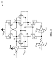
- FIG. 2 shows a level shifter apparatus 200, in accordance with another example embodiment.
- the schematic is shown as implemented for signal conversion from a bottom domain to a top domain, with the understanding that a complementary circuit may be implemented for signal conversion from a top to a bottom domain.
- Inverters I1 and I2 are in the bottom voltage domain while transistors (e.g. , PMOS) M7, M8 and inverter I3 are in the top voltage domain.
- Transistors M1-M6 are shared between the top and bottom domains.
- the '1' (high) logic value of the bottom domain has the same voltage level as '0' (low) of the top domain, represented by V mid .
- Signals are transferred between domains as follows. For an initial signal 'A' and 'X' are at respective '0' (low) logic values, nodes M, N are '1' (high) and M', N' are '0' (low).
- signal 'A' changes state, ( e.g., goes from '0' (low) to '1' (high) logic value), the output of I1 goes to '0' (low), and the output of I2 goes to '1' (high) of the bottom voltage domain.
- the state of the latch is flipped by the pull-down action of either M1, M3, and M5 competing with M7, or by M2, M4, and M6 competing with M8.
- the dimensioning of these transistors can be set to achieve desirable operation.
- Figure 3 shows plots of the operation of a level shifter with transition from low to high and from high to low, in accordance with one or more embodiments.
- the plots in Figure 3 may be implemented with the circuit shown in Figure 2 or other circuits operating under a similar approach. Time is shown in nanoseconds on the horizontal axis, and voltage is shown in volts on the vertical axis.
- Plot 310 shows an input signal
- plot 320 shows an output signal that is a level-shifted version of the input signal.
- a complimentary version in which a signal is transferred from a top voltage domain to low voltage domain can also be realized in a similar manner. Further, such approaches can be extended to multiple domains in addition to the two domains shown.
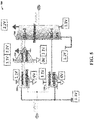
- FIG. 4 shows an apparatus 400, as may be implemented in accordance with one or more embodiments.
- the apparatus 400 includes level shifter circuitry 410 that operates to communicate signals between first power domain circuitry 420 and second power domain circuitry 430.
- Each of the power domains is coupled between respective power rails depicted as VDD and GND (e.g., a reference voltage level), with the first power domain operating between VDD1 and GND1, and the second power domain operating between VDD2 and GND2.
- VDD and GND e.g., a reference voltage level
- the level shifter 410 operates to actively control the coupling of VDD1 to GND2 for a stacked mode, or the coupling of VDD2 to GND1 for another stacked mode.
- the level shifter 410 couples VDD1 to VDD2, and GND1 to GND2.
- the level shifter 410 includes a shift circuit 414 and a bypass circuit 416 that respectively operate to shift the level of signals passed between the power domains, or bypass the shift circuit such that the level of the signals is not shifted.
- a multiplexer 418 may be employed to multiplex the respective circuit paths including the shift circuit 414 and the bypass circuit 416, as may be controlled or otherwise operated in accordance with the range detection/comparison circuitry 412.
- one or more embodiments employ a detection approach as follows.
- Other embodiments may involve a comparison of VDD1 with VDD2, with a stacked architecture detected when the levels are different.
- the circuit 600 similarly includes an AND cell 610 and a level shifter 620 in a first circuit path, and an isolation (OR) cell 630 in a second circuit path, both of which are connected to multiplexer 640.
- the respective circuits 500 and 300 may be implemented in a common circuit for respective modes.
- a 1.1 V voltage range is shown for respective power domains (e.g. , VDD1 at 2.2V, GND1 at 1.1V, and VDD2 at 1.1V, GND2 at 0V), in which translation between voltage levels of domains in a stacked mode and a bypass mode are provided.
- VDD1 at 2.2V an output of level shifter 520 is selected via AND circuit 510.
- a bypass circuit is selected via OR circuit 630. This selection can be done without using external control signals.
- the voltage information of the opposite domain is used.
- the select signal is still at 1.1V, which equals a logical '1' since the top/high domain is between 0V and 1.1V under which conditions the bypass path is selected.
- 0V and 1.1V can be implemented as first and second voltage levels between which the top/high domain operates. Different explicit voltages may also be used in various implementations (with both the above and following discussion).
- the ground rail of the top/high power domain is 1.1 V and provides a logical '1' in the bottom/low power domain (0-1.1V).
- the OR isolation cell 530 forces an output to 1.1V, while the AND isolation cell 510 is sensitive to the input signal level and buffers it for the level shifter input.
- the level shifter receives the input signal and converts it to the desired voltage levels.
- the ground voltage of the top/high power domain that controls the two isolation cells is at 0V, which is a logical '0' in the bottom/lower power domain (also 0-1.1V in flat mode).
- a logical '0' will force the output of the AND isolation cell 610 to 0V while enabling the OR isolation cell 630 to bypass the signal to the multiplexer 640.
- Figure 7 shows an up-level shifter 700, in accordance with another embodiment.
- GND2 and VDD1 are the same.
- the up-level shifter 700 may, for example, be implemented in a manner similar to that of the level shifter apparatus 200 in Figure 2 .
- the above discussion of Figure 2 may be generally applied in Figure 7 .
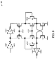
- Figure 8 shows a down-level shifter 800, in accordance with another example embodiment.
- the voltage of GND 1 and VDD2 are the same.
- the down-level shifter 800 may, for example, be implemented in a manner similar to that of the level shifter apparatus 200 in Figure 2 , or as a corollary to Figure 7 (similarly shifting, but from high to low, rather than from low to high).
- the above discussion of Figure 2 may be generally applied in Figure 8 .
- the voltage levels of the respective components in Figures 7 and 8 are implemented in accordance with the following Table 1, for stacked and flat power modes.
- Table 1 First (Stacked) Power Mode Second (Flat) Power Mode Up level shifter Down level shifter Up level shifter Down level shifter GND1 V1 V2 V1 V1 VDD1 V2 V3 V2 V2 GND2 V2 V1 V1 V1 VDD2 V3 V2 V2 V2 V1: First voltage level V2: Second voltage level V3: Third voltage level
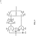
- Figure 9 shows an up-level shifter 900 for a stacked power mode, in accordance with one or more embodiments.
- the up-level shifter 900 may, for example, be implemented in connection with the approach characterized in Figures 4 , 5 and/or 6.
- An AND gate 910 provides an output to level shifter 920, which is output by multiplexer 940 under the stacked mode.
- An OR gate 930 operates to pass an output to the multiplexer 940 for a flat mode.
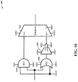
- Figure 10 shows a down-level shifter 1000, in accordance with one or more embodiments.
- the down-level shifter 1000 may, for example, be implemented in connection with the approach characterized in Figures 4 , 5 and/or 6.
- An OR gate 1030 operates in a stacked mode to couple a signal to a level shifter 1020, which provides an output to multiplexer 1040 that selects the (down-shifted) output.
- An AND gate 1010 operates in a flat mode to couple and output to the multiplexer 1040.
- a "block” also sometimes “circuit”, “logic circuitry”, or “module”
- a circuit that carries out one or more of these or related operations/activities.
- Such an approach can be used, for example, with blocks as shown in Figure 1 .
- a hard-wired control block can be used for such an implementation.
- one or more modules are discreet logic circuits or programmable logic circuits configured and arranged for implementing these operations/activities.
- circuits as shown in Figure 2 may be implemented with different circuitry to achieve related functionality.
- additional level shifters may be implemented to serve additional power domains, with more or fewer circuits operating for communicating signals therebetween, and operating at voltage ranges that may be tailored to each circuit.
- Various embodiments may be implemented in manners different than those illustrated by the Figures. For instance, level shifting may be carried out in a manner similar to that characterized in U.S. Patent Application Serial No. 13/856,184 . Such modifications do not depart from the true spirit and scope of various aspects of the invention, including aspects set forth in the claims.
Landscapes
- Engineering & Computer Science (AREA)
- Computer Hardware Design (AREA)
- Physics & Mathematics (AREA)
- Computing Systems (AREA)
- General Engineering & Computer Science (AREA)
- Mathematical Physics (AREA)
- Nonlinear Science (AREA)
- Logic Circuits (AREA)
Applications Claiming Priority (1)
| Application Number | Priority Date | Filing Date | Title |
|---|---|---|---|
| US14/794,411 US9917588B2 (en) | 2015-07-08 | 2015-07-08 | Level shifter and approach therefor |
Publications (2)
| Publication Number | Publication Date |
|---|---|
| EP3116128A2 true EP3116128A2 (de) | 2017-01-11 |
| EP3116128A3 EP3116128A3 (de) | 2017-04-19 |
Family
ID=56148226
Family Applications (1)
| Application Number | Title | Priority Date | Filing Date |
|---|---|---|---|
| EP16175288.6A Withdrawn EP3116128A3 (de) | 2015-07-08 | 2016-06-20 | Pegelschieber und ansatz dafür |
Country Status (3)
| Country | Link |
|---|---|
| US (1) | US9917588B2 (de) |
| EP (1) | EP3116128A3 (de) |
| CN (1) | CN106341116A (de) |
Families Citing this family (18)
| Publication number | Priority date | Publication date | Assignee | Title |
|---|---|---|---|---|
| US9912335B2 (en) | 2015-07-08 | 2018-03-06 | Nxp B.V. | Configurable power domain and method |
| JP2017073742A (ja) * | 2015-10-09 | 2017-04-13 | 株式会社東芝 | レベルシフト回路、半導体装置および電池監視装置 |
| JP6817081B2 (ja) * | 2017-01-17 | 2021-01-20 | エイブリック株式会社 | レベルシフト回路 |
| US10158292B2 (en) | 2017-01-23 | 2018-12-18 | Nxp B.V. | Power configuration |
| JP2018129727A (ja) * | 2017-02-09 | 2018-08-16 | エイブリック株式会社 | レベルシフタ |
| CN108736878B (zh) * | 2017-04-13 | 2022-01-25 | 华邦电子股份有限公司 | 电压电平移位器 |
| IT201700096772A1 (it) * | 2017-08-29 | 2019-03-01 | St Microelectronics Srl | Circuito traslatore di livello, dispositivo e procedimento corrispondenti |
| CN107634752B (zh) * | 2017-09-20 | 2024-07-16 | 北京集创北方科技股份有限公司 | 驱动装置和驱动方法 |
| US10270448B1 (en) * | 2018-05-16 | 2019-04-23 | Nxp B.V. | Level shifter circuit with transistor drive strength variation compensation |
| KR102519602B1 (ko) * | 2018-12-17 | 2023-04-07 | 에스케이하이닉스 주식회사 | 레벨 쉬프터 및 이를 포함하는 드라이버 회로 |
| US10892750B2 (en) | 2018-05-31 | 2021-01-12 | SK Hynix Inc. | Semiconductor apparatus |
| US10622975B2 (en) * | 2018-06-11 | 2020-04-14 | Semiconductor Components Industries, Llc | Voltage translator using low voltage power supply |
| US10277226B1 (en) * | 2018-06-11 | 2019-04-30 | Semiconductor Components Industries, Llc | Voltage translator device |
| US11831153B1 (en) | 2019-05-03 | 2023-11-28 | Cadence Design Systems, Inc. | High-bandwidth signal driver/receiver |
| EP3813261B1 (de) * | 2019-10-25 | 2024-12-11 | Nxp B.V. | Vorrichtung mit einem pegelschieber |
| US11921651B2 (en) * | 2021-06-07 | 2024-03-05 | AyDeeKay LLC | Interface module with low-latency communication of electrical signals between power domains |
| US12027120B2 (en) * | 2021-09-17 | 2024-07-02 | Apple Inc. | Ground isolation systems and methods |
| CN117097324B (zh) * | 2023-09-04 | 2024-05-31 | 中科赛飞(广州)半导体有限公司 | 一种电平转移电路 |
Citations (1)
| Publication number | Priority date | Publication date | Assignee | Title |
|---|---|---|---|---|
| US20140300188A1 (en) | 2013-04-03 | 2014-10-09 | Nep B.V. | Capacitive level shifter devices, methods and systems |
Family Cites Families (30)
| Publication number | Priority date | Publication date | Assignee | Title |
|---|---|---|---|---|
| JP3300593B2 (ja) | 1995-06-15 | 2002-07-08 | 株式会社東芝 | 半導体集積回路装置 |
| JP2002197881A (ja) | 2000-12-27 | 2002-07-12 | Toshiba Corp | レベルシフタ及びレベルシフタを備えた半導体記憶装置 |
| US6479974B2 (en) | 2000-12-28 | 2002-11-12 | International Business Machines Corporation | Stacked voltage rails for low-voltage DC distribution |
| US6803801B2 (en) | 2002-11-07 | 2004-10-12 | Lsi Logic Corporation | CMOS level shifters using native devices |
| US7329968B2 (en) | 2003-05-08 | 2008-02-12 | The Trustees Of Columbia University In The City Of New York | Charge-recycling voltage domains for energy-efficient low-voltage operation of digital CMOS circuits |
| US20050134355A1 (en) * | 2003-12-18 | 2005-06-23 | Masato Maede | Level shift circuit |
| US7002371B2 (en) | 2003-12-29 | 2006-02-21 | Freescale Semiconductor, Inc. | Level shifter |
| US7702929B2 (en) | 2004-11-29 | 2010-04-20 | Marvell World Trade Ltd. | Low voltage logic operation using higher voltage supply levels |
| US7449918B2 (en) * | 2005-12-22 | 2008-11-11 | Panasonic Corporation | Level shift circuit |
| US7696786B2 (en) * | 2006-03-06 | 2010-04-13 | On Semiconductor | Precision differential level shifter |
| JP2009533929A (ja) * | 2006-04-12 | 2009-09-17 | エヌエックスピー ビー ヴィ | 電子回路 |
| US8228092B2 (en) | 2006-09-15 | 2012-07-24 | Texas Instruments Northern Virginia Incorporated | High voltage latching and DC restoration isolation and level shifting method and apparatus |
| US7804327B2 (en) * | 2007-10-12 | 2010-09-28 | Mediatek Inc. | Level shifters |
| US7683696B1 (en) * | 2007-12-26 | 2010-03-23 | Exar Corporation | Open-drain output buffer for single-voltage-supply CMOS |
| US20090206878A1 (en) * | 2008-02-14 | 2009-08-20 | Himax Technologies Limited | Level shift circuit for a driving circuit |
| JP5247240B2 (ja) * | 2008-05-22 | 2013-07-24 | キヤノン株式会社 | 集積回路、集積回路を備える電子機器 |
| CN101674072B (zh) * | 2008-09-10 | 2011-10-05 | 中国科学院半导体研究所 | 一种用于低电压差分信号接收的接口电路 |
| US7847590B2 (en) * | 2008-11-03 | 2010-12-07 | Agilent Technologies, Inc. | Level shifter including cascode sets |
| US8174288B2 (en) | 2009-04-13 | 2012-05-08 | International Business Machines Corporation | Voltage conversion and integrated circuits with stacked voltage domains |
| CN101938271B (zh) * | 2009-06-29 | 2012-07-18 | 上海电器股份有限公司人民电器厂 | 一种微电流/电压转换信号调理电路 |
| US8169257B2 (en) | 2009-11-18 | 2012-05-01 | Freescale Semiconductor, Inc. | System and method for communicating between multiple voltage tiers |
| US8476962B2 (en) | 2009-11-18 | 2013-07-02 | Freescale Semiconductor, Inc. | System having multiple voltage tiers and method therefor |
| CN101866635B (zh) * | 2010-05-27 | 2012-08-08 | 旭曜科技股份有限公司 | 转压器 |
| US8547140B1 (en) | 2010-11-03 | 2013-10-01 | Pmc-Sierra, Inc. | Apparatus and method for generating a bias voltage |
| US8704579B2 (en) * | 2011-12-30 | 2014-04-22 | Taiwan Semiconductor Manufacturing Company, Ltd. | Level shifting circuit and semiconductor device using the same |
| US8878387B1 (en) | 2013-05-16 | 2014-11-04 | Micrel, Inc. | Multi-level stack voltage system for integrated circuits |
| JP6149677B2 (ja) | 2013-10-10 | 2017-06-21 | 富士通株式会社 | レベルシフタ及びdc−dcコンバータ |
| KR101531887B1 (ko) * | 2013-11-27 | 2015-06-26 | 주식회사 동부하이텍 | 네거티브 레벨 쉬프터 |
| US20150346742A1 (en) | 2014-06-02 | 2015-12-03 | Nxp B.V. | Energy recycling for a cost effective platform to optimize energy efficiency for low powered system |
| US9912335B2 (en) | 2015-07-08 | 2018-03-06 | Nxp B.V. | Configurable power domain and method |
-
2015
- 2015-07-08 US US14/794,411 patent/US9917588B2/en active Active
-
2016
- 2016-06-20 EP EP16175288.6A patent/EP3116128A3/de not_active Withdrawn
- 2016-07-05 CN CN201610524215.2A patent/CN106341116A/zh not_active Withdrawn
Patent Citations (1)
| Publication number | Priority date | Publication date | Assignee | Title |
|---|---|---|---|---|
| US20140300188A1 (en) | 2013-04-03 | 2014-10-09 | Nep B.V. | Capacitive level shifter devices, methods and systems |
Also Published As
| Publication number | Publication date |
|---|---|
| CN106341116A (zh) | 2017-01-18 |
| US9917588B2 (en) | 2018-03-13 |
| US20170012628A1 (en) | 2017-01-12 |
| EP3116128A3 (de) | 2017-04-19 |
Similar Documents
| Publication | Publication Date | Title |
|---|---|---|
| US9917588B2 (en) | Level shifter and approach therefor | |
| EP3115869B1 (de) | Domäne mit konfigurierbarer leistung und verfahren | |
| US9257973B1 (en) | Supply-state-enabled level shifter interface circuit and method | |
| US8228092B2 (en) | High voltage latching and DC restoration isolation and level shifting method and apparatus | |
| EP0614279B1 (de) | Überspannungstolerante Ausgangspufferschaltung | |
| US5406140A (en) | Voltage translation and overvoltage protection | |
| EP0702860B1 (de) | Überspannungsschutz | |
| US5896045A (en) | Static pulsed cross-coupled level shifter and method therefor | |
| US8659341B2 (en) | System and method for level-shifting voltage signals using a dynamic level-shifting architecture | |
| US11139843B1 (en) | SerDes driver with common-gate-based buffer to use core devices in relatively high power supply domain | |
| US7750687B2 (en) | Circuit arrangement comprising a level shifter and method | |
| US9537469B2 (en) | CMOS level shifter with reduced high voltage transistor count | |
| EP1369999A1 (de) | Pegelverschiebungsschaltung mit asymmetrischem Eingang | |
| CN102055459B (zh) | 在保险/容限操作期间产生偏压以保护输入/输出电路 | |
| US8471803B2 (en) | Level shifters including circuitry for reducing short circuits and display devices using the same | |
| CN115865074A (zh) | 电平转换电路、射频开关控制电路和射频前端模组 | |
| JP2010164877A (ja) | 表示パネルドライバ、表示装置、及び表示パネルドライバの動作方法 | |
| EP2011236B1 (de) | Elektronische schaltung | |
| US6518790B2 (en) | Semiconductor integrated circuit having circuit for transmitting input signal | |
| KR101830302B1 (ko) | 데이터 구동 증폭기 | |
| CN114095004A (zh) | 驱动电路 | |
| US12199606B2 (en) | Level shifter with expanded voltage range | |
| CN102118170A (zh) | D/a转换器电路及其电压供给控制方法 | |
| US20100134146A1 (en) | Voltage level translator and method | |
| WO2004066259A1 (ja) | ラッチ、ラッチの駆動方法、フラットディスプレイ装置 |
Legal Events
| Date | Code | Title | Description |
|---|---|---|---|
| PUAI | Public reference made under article 153(3) epc to a published international application that has entered the european phase |
Free format text: ORIGINAL CODE: 0009012 |
|
| AK | Designated contracting states |
Kind code of ref document: A2 Designated state(s): AL AT BE BG CH CY CZ DE DK EE ES FI FR GB GR HR HU IE IS IT LI LT LU LV MC MK MT NL NO PL PT RO RS SE SI SK SM TR |
|
| AX | Request for extension of the european patent |
Extension state: BA ME |
|
| PUAL | Search report despatched |
Free format text: ORIGINAL CODE: 0009013 |
|
| AK | Designated contracting states |
Kind code of ref document: A3 Designated state(s): AL AT BE BG CH CY CZ DE DK EE ES FI FR GB GR HR HU IE IS IT LI LT LU LV MC MK MT NL NO PL PT RO RS SE SI SK SM TR |
|
| AX | Request for extension of the european patent |
Extension state: BA ME |
|
| RIC1 | Information provided on ipc code assigned before grant |
Ipc: H03K 19/0185 20060101ALI20170314BHEP Ipc: H03K 5/13 20140101AFI20170314BHEP |
|
| STAA | Information on the status of an ep patent application or granted ep patent |
Free format text: STATUS: THE APPLICATION IS DEEMED TO BE WITHDRAWN |
|
| 18D | Application deemed to be withdrawn |
Effective date: 20171020 |