EP3120460B1 - Puces comprenant des processeurs informatiques classique et quantique - Google Patents
Puces comprenant des processeurs informatiques classique et quantique Download PDFInfo
- Publication number
- EP3120460B1 EP3120460B1 EP15765127.4A EP15765127A EP3120460B1 EP 3120460 B1 EP3120460 B1 EP 3120460B1 EP 15765127 A EP15765127 A EP 15765127A EP 3120460 B1 EP3120460 B1 EP 3120460B1
- Authority
- EP
- European Patent Office
- Prior art keywords
- quantum
- classical
- computing processor
- processor
- qubits
- Prior art date
- Legal status (The legal status is an assumption and is not a legal conclusion. Google has not performed a legal analysis and makes no representation as to the accuracy of the status listed.)
- Active
Links
Images




Classifications
-
- G—PHYSICS
- G06—COMPUTING OR CALCULATING; COUNTING
- G06F—ELECTRIC DIGITAL DATA PROCESSING
- G06F13/00—Interconnection of, or transfer of information or other signals between, memories, input/output devices or central processing units
- G06F13/38—Information transfer, e.g. on bus
- G06F13/40—Bus structure
- G06F13/4063—Device-to-bus coupling
- G06F13/4068—Electrical coupling
-
- G—PHYSICS
- G06—COMPUTING OR CALCULATING; COUNTING
- G06F—ELECTRIC DIGITAL DATA PROCESSING
- G06F15/00—Digital computers in general; Data processing equipment in general
- G06F15/76—Architectures of general purpose stored program computers
- G06F15/80—Architectures of general purpose stored program computers comprising an array of processing units with common control, e.g. single instruction multiple data processors
-
- G—PHYSICS
- G06—COMPUTING OR CALCULATING; COUNTING
- G06N—COMPUTING ARRANGEMENTS BASED ON SPECIFIC COMPUTATIONAL MODELS
- G06N10/00—Quantum computing, i.e. information processing based on quantum-mechanical phenomena
- G06N10/20—Models of quantum computing, e.g. quantum circuits or universal quantum computers
-
- G—PHYSICS
- G06—COMPUTING OR CALCULATING; COUNTING
- G06N—COMPUTING ARRANGEMENTS BASED ON SPECIFIC COMPUTATIONAL MODELS
- G06N10/00—Quantum computing, i.e. information processing based on quantum-mechanical phenomena
- G06N10/40—Physical realisations or architectures of quantum processors or components for manipulating qubits, e.g. qubit coupling or qubit control
-
- G—PHYSICS
- G06—COMPUTING OR CALCULATING; COUNTING
- G06N—COMPUTING ARRANGEMENTS BASED ON SPECIFIC COMPUTATIONAL MODELS
- G06N10/00—Quantum computing, i.e. information processing based on quantum-mechanical phenomena
- G06N10/60—Quantum algorithms, e.g. based on quantum optimisation, quantum Fourier or Hadamard transforms
-
- H—ELECTRICITY
- H01—ELECTRIC ELEMENTS
- H01P—WAVEGUIDES; RESONATORS, LINES, OR OTHER DEVICES OF THE WAVEGUIDE TYPE
- H01P5/00—Coupling devices of the waveguide type
- H01P5/08—Coupling devices of the waveguide type for linking dissimilar lines or devices
-
- H—ELECTRICITY
- H03—ELECTRONIC CIRCUITRY
- H03K—PULSE TECHNIQUE
- H03K19/00—Logic circuits, i.e. having at least two inputs acting on one output; Inverting circuits
- H03K19/02—Logic circuits, i.e. having at least two inputs acting on one output; Inverting circuits using specified components
- H03K19/195—Logic circuits, i.e. having at least two inputs acting on one output; Inverting circuits using specified components using superconductive devices
-
- H—ELECTRICITY
- H10—SEMICONDUCTOR DEVICES; ELECTRIC SOLID-STATE DEVICES NOT OTHERWISE PROVIDED FOR
- H10N—ELECTRIC SOLID-STATE DEVICES NOT OTHERWISE PROVIDED FOR
- H10N60/00—Superconducting devices
- H10N60/10—Junction-based devices
- H10N60/12—Josephson-effect devices
-
- H—ELECTRICITY
- H10—SEMICONDUCTOR DEVICES; ELECTRIC SOLID-STATE DEVICES NOT OTHERWISE PROVIDED FOR
- H10N—ELECTRIC SOLID-STATE DEVICES NOT OTHERWISE PROVIDED FOR
- H10N60/00—Superconducting devices
- H10N60/80—Constructional details
- H10N60/805—Constructional details for Josephson-effect devices
-
- H—ELECTRICITY
- H10—SEMICONDUCTOR DEVICES; ELECTRIC SOLID-STATE DEVICES NOT OTHERWISE PROVIDED FOR
- H10N—ELECTRIC SOLID-STATE DEVICES NOT OTHERWISE PROVIDED FOR
- H10N69/00—Integrated devices, or assemblies of multiple devices, comprising at least one superconducting element covered by group H10N60/00
-
- Y—GENERAL TAGGING OF NEW TECHNOLOGICAL DEVELOPMENTS; GENERAL TAGGING OF CROSS-SECTIONAL TECHNOLOGIES SPANNING OVER SEVERAL SECTIONS OF THE IPC; TECHNICAL SUBJECTS COVERED BY FORMER USPC CROSS-REFERENCE ART COLLECTIONS [XRACs] AND DIGESTS
- Y02—TECHNOLOGIES OR APPLICATIONS FOR MITIGATION OR ADAPTATION AGAINST CLIMATE CHANGE
- Y02D—CLIMATE CHANGE MITIGATION TECHNOLOGIES IN INFORMATION AND COMMUNICATION TECHNOLOGIES [ICT], I.E. INFORMATION AND COMMUNICATION TECHNOLOGIES AIMING AT THE REDUCTION OF THEIR OWN ENERGY USE
- Y02D10/00—Energy efficient computing, e.g. low power processors, power management or thermal management
Definitions
- Artificial intelligence tasks can be translated into machine learning optimization problems. Some simplified tasks, such as feed forward problems, can be carried out by classical processors. Other complicated tasks, such as those involving NP-hard problems, can be performed using quantum hardware, e.g., a quantum processor.
- a quantum processor is constructed and programmed to encode the solution to a corresponding machine optimization problem into an energy spectrum of a many- body quantum Hamiltonian characterizing the quantum hardware. For example, the solution is encoded in the ground state of the Hamiltonian. Through an annealing process in which the Hamiltonian evolves from an initial Hamiltonian into a problem Hamiltonian, the energy spectrum or the ground state of the Hamiltonian for solving the problem can be obtained without diagonalizing the Hamiltonian.
- the present disclosure relates to chips that include both classical and quantum computing processors. Accordingly, the present invention provides an apparatus according to claim 1. Preferred embodiments are defined in the dependent claims.
- the present invention may have one or more advantages. For example, combining classical computing processors and quantum computing processors on a single chip enables improvements in energy-efficiency of the overall system. By placing both the quantum and classical processor on a single chip that is cooled to temperatures applicable to achieve superconductivity within the classical processor's circuit components as well as the coupling components, the amount of heat dissipation through the classical processor circuit components and coupling components can be reduced. To assist with energy minimization, the same base material (e.g. Niobium or Aluminum) that is used for the quantum processor can be used for the electronic components of the classical processor, thus establishing a single critical temperature that is needed to achieve superconductivity.
- Niobium or Aluminum the same base material that is used for the quantum processor can be used for the electronic components of the classical processor, thus establishing a single critical temperature that is needed to achieve superconductivity.
- Reciprocal Quantum Logic combines features of CMOS fabrication methodology (e.g., techniques such as micro and nano-lithography, photo-development, etching, lift-off, among others) with high speed and low-power signal levels achievable using Single-Flux Quantum signals, allowing for low static power dissipation, low latency and combinational logic.
- the heat dissipation reduction can be theoretically estimated to lead to substantial savings in energy consumption of up to approximately eight orders of magnitude. This estimation is based on the energy-scale separation between existing CMOS semiconductors-based transistors with the fundamental Landauer limit of energy dissipation of computation that is allowable under the known laws of physics. Moreover, as the energy efficiency and consumption of classical processors operating above a superconducting critical temperature (e.g., CMOS-based) continues to increase with Moore's law, the increases in energy efficiency associated with classical processors operating on the same chip as the quantum processor become more desirable.
- CMOS-based superconducting critical temperature
- the output of a classical algorithm run by the classical processor can be used as a seed to a quantum algorithm run by the quantum processor and the output of the quantum algorithm (e.g., that employs quantum annealing after measurement in computational basis) can be feed-forwarded to a classical algorithm for post-processing.
- This mechanism can be implemented iteratively and could lead to substantial improvements in computational speed, especially when the problem Hamiltonian has degenerate global energy with highly rigid local landscapes (e.g., with tall barriers that can utilize non-local features of quantum trajectories or quantum jumps).
- Combining the quantum and classical processors on the same chip can reduce the number of communication channels and control lines in and/or out of the combined chip. Moreover, placing classical and quantum processors on the same chip can reduce the distance between the processors. As a result, there may be associated increases in signal strength and/or improvement in the fidelity of state transfer. Additionally, the occurrence of decoherence of the quantum processor can be reduced. In the context of quantum annealing, this passive error-avoidance architecture is significant as there is not yet any known active error-correction strategy for such systems, in contrast to digital or gate-model quantum computing proposals.
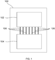
- FIG. 1 is a schematic that illustrates an example of a single chip 100 on which is formed a classical computing processor 102 and a quantum computing processor 104.
- the classical computing processor 102 can exchange data with the quantum computing processor 104 through couplers 106.
- the classical computing processor 102 may be configured to carry out instructions of a computer program by performing basic arithmetical, logical, and input/output operations on data, in which the data is represented in analog or digital form.
- the processor 102 may be constructed of active and passive electrical components that are configured, in part or as a whole, to execute a series of operations/tasks for manipulating one or more inputs to obtain one or more outputs, and achieve a desired end-result.
- the quantum computing processor 104 may be configured to make use of quantum-mechanical phenomena, such as superposition and entanglement, to perform operations on data in a non-deterministic manner.
- the quantum computing processor 104 is configured to represent information in more than one state simultaneously (e.g., as qubits).
- the chip 100 can be used to perform tasks that are carried out only by the classical computing processor 102, tasks that are carried out only by the quantum computing processor 104, or tasks that are carried out by a combination of the classical computing processor 102 and the quantum computing processor 104.
- the output of the classical computing processor 102 can be provided to the quantum computing processor 104 as input through the couplers 106.
- the output of the quantum computing processor 104 can be provided to the classical computing processor 102 through the couplers 106.
- the chip 100 includes multiple classical computing processors 102 and/or multiple quantum computing processors 104, in which one or more classical computing processors 102 exchange data with one or more quantum computing processors 104 through couplers 106.
- the components of the processor 104 can be driven with a transverse magnetic field to create quantum mechanical superposition and multi-qubit dissipative quantum tunneling in a given quantum annealing schedule.
- the components of the processor 102 can be driven with zero or negligible transverse field that allows for dominating thermal excitation and implementation of a classical algorithm such as Simulated Annealing (SA), Metropolis-Hasting algorithm or Spin Vector Monte Carlo (SVMC).
- SA Simulated Annealing
- SVMC Spin Vector Monte Carlo
- both the classical computing processor 102 and the quantum computing processor 104 may be formed on the same chip. For instance, combining the classical computing processor 102 and the quantum computing processor 104 on a single chip may minimize energy consumption of the system as a whole. By placing both the quantum and classical processor on a single chip that is cooled to temperatures applicable to achieve superconductivity within the classical processor's circuit components as well as the coupling components, it is possible, in certain example implementations, to reduce the amount of heat dissipation through the classical processor circuit components and coupling components. In some example implementations, different elements of the classical computing processor 104 consume less power than equivalent device that operate at room temperature and also may generate less waste heat.
- the same fabrication techniques can be used to manufacture the quantum processor components and the classical processor components on the same substrate.
- the same lithography, etching and deposition steps for building quantum annealing hardware, such as multi-qubit superconducting flux qubits, can be used for building the classical processor components, reducing the overall number of fabrication steps for the system.
- the classical computing processor 102 operates on the same cooled substrate as the quantum computing processor 104, no additional and separate cooling mechanism for the classical processor 102 may be required. Instead, the cooling process used to maintain the quantum processor 104 at its operating temperature (e.g., dilution refrigerator) can also be used to cool the classical processor 102.
- the cooling process used to maintain the quantum processor 104 at its operating temperature e.g., dilution refrigerator
- combining the classical processor 102 and the quantum processor 104 on a single chip also may improve the signal to noise ratio of data transferred between the two computing processors.
- the distance over which the data travels between the two processors can be reduced, which may lead to a corresponding reduction in noise.
- one or more closed-loop quantum control mechanisms can be performed coherently on the chip with the appropriate feedback mechanism.
- there the number of classical control lines for coupling data into and/or out of the chip can be reduced. This reduction in classical control lines can suppress unwanted interactions of random environmental effects such as phononic and photonic radiation bath and systematic control errors that have a higher probability of occurring in the classical control lines.
- the classical computing processor 102 may operate on data in combination with the quantum computing processor 104 to solve one or more problems.
- the classical processor 102 is configured to output data that serves to initialize, or "seed" the quantum computing processor 104 (e.g., to initialize a Hamiltonian of the quantum processor 104).
- the quantum processor 104 solves problems that are otherwise computationally intractable for the classical processor 102, where the output of the quantum processor 104 may be fed back to the classical processor 102.
- FIG. 2 is a schematic illustrating an example of a classical computing processor 200, such as the processor 102 shown in FIG. 1 , in which the processor 200 is formed on the same chip as a quantum computing processor.
- the classical computing processor 200 is constructed using superconducting materials.
- the classical computing processor 200 includes 4 by 4 unit cells 202 of eight electronic components 204, in which each active component 204 is capable of generating a binary bit (e.g., 1 or 0, -1 or +1).
- the bits generated by components 204 are connected by inductive couplers as shown by lines 206.
- Each line 206 may represent one or multiple couplers between a pair of bits.
- the bits produced by components 204 and the couplers 206 can be thought of as the vertices and edges, respectively, of a "Chimera" graph with a bipartite structure.
- the processor 200 can also include a larger number of unit cells 202, e.g., 8 by 8 or more.
- RQL Reciprocal Quantum Logic
- CMOS complementary metal-oxide-semiconductor
- SFQ Single Flux Quanta
- the SFQ can exist as a transient voltage pulse across the Josephson junction or as a persistent current in a superconducting inductive loop.
- Various high speed processors have been constructed using SFQ including, for example, a static digital divider that operates up to 770 GHz, a digital signal processor operating between 20-40 GHz, and a serial microprocessor operating at 20 GHz.
- DC power was delivered on a common voltage rail via bias resistors, analogous to TTL logic, which lead to parasitic heat and increased latency.
- RQL is able to reduce the parasitic heat and latencies by replacing bias resistors with inductive coupling to an AC transmission line.
- RQL encodes data (e.g., a logical "1") as a reciprocal pair of SFQ pulses of opposite polarity.
- data e.g., a logical "1
- the logic operation involves storage and routing of SFQ data pulses.
- the trailing negative polarity pulse acts as a reset.
- the active components 204 of the classical processor 200 can be built using the same superconducting electronic components (e.g., SQUID devices, see below) of the quantum processor, in which the dynamics of each component is driven to a classical limit (e.g., by eliminating the transverse magnetic field at a finite temperature of the overall unit).
- the classical processor is a probabilistic analog device that could implement probabilistic inference and optimization algorithm such as belief propagation, simulated annealing, spin-vector Monte Carlo.
- the components of the classical processor may be formed of the same material (e.g., superconducting metals such as aluminum, niobium, lead alloys, or other applicable metals) used to form the quantum processor on the chip.
- the classical computing processor can be formed using multiple layers of a superconducting metal such as Niobium, deposited on a substrate (e.g., Si) where different components (e.g., coupling inductors, Josephson junctions, bias inductors, clock lines) are formed in one or more layers using standard micro and nano-lithography techniques.
- a Josephson junction can be formed, for example, by separating the superconductor metal with a thin insulating barrier (e.g., with an oxide insulator such as aluminum oxide or niobium oxide) or a short section of non-superconducting metal.
- a bit shift register can be fabricated, for example, with 1600 Josephson junctions in a commercial superconductor fabrication process with 4.5 kA cm -2 Josephson junction critical current density, 1.5 ⁇ m minimum feature size, and four metal layers.
- FIG. 3 is a schematic illustrating an example of a quantum computing processor 300, such as the processor 104 shown in FIG. 1 , in which the processor 300 is formed on the same chip as a classical computing processor.
- the processor 300 may include any suitable quantum computing system such as, for example, a superconducting adiabatic quantum computing (AQC) systems
- the quantum processor 300 includes 4 by 4 unit cells 302 of eight components 304 that are operable to generate qubits.
- Programmable inductive couplers 306, shown by lines in FIG. 3 connect different qubits within a unit cell and across different unit cells. Each line 306 can correspond to one or multiple couplers between a pair of qubits.
- the processor 300 can also include a larger number of unit cells 302, e.g., 8 by 8 or more.
- the qubits produced by components 304 and the couplers 306 can be thought of as the vertices and edges, respectively, of a "Chimera" graph with a bipartite structure.
- the components 304 of the quantum computing processor 300 can be constructed from superconducting electronic circuits (e.g., superconducting quantum interference devices (SQUIDs)).
- the superconducting electronic circuits a quantum computing processor are operated at very low temperatures, such as on the order of 1 K or less, so that superconductivity is realized for the selected superconducting material, and thermal fluctuations do not cause transitions between energy levels.
- SQUIDs can be formed from at least one metal (e.g., Niobium, Aluminum, or a lead alloy), in which the SQUID operates below the metal's corresponding critical temperature threshold for superconductivity.
- a typical implementation of a SQUID includes a ring of superconductor metal interrupted by one or more Josephson junctions or capacitors.
- a Josephson junction can be formed, for example, by separating the superconductor metal with a thin insulating barrier (e.g., with an oxide insulator such as aluminum oxide) or a short section of non-superconducting metal.
- electric charge may pass through the Josephson junction of the SQUID through the process of quantum tunneling.
- the information in a SQUID can be encoded, for example, as an electric charge, a phase or flux (e.g., as a result of combinatory possibilities of cooper-pairs current in various superconducting islands).
- the state of various SQUIDs can be quantum-mechanically entangled by either inductive couplings, capacitor couplings, or Cavity quantum electrodynamics (QED) transmission lines.
- QED Cavity quantum electrodynamics
- the measurement of quantum state and dynamics of qubits can be performed by entangling the state of each SQUID with photonic excitations in one or several transmission lines, in which the photonic excitations are injected electronically.
- the quantum processor can be formed using multiple layers of a superconducting metal such as Niobium, deposited on a substrate (e.g., Si) where different components of the processor (e.g., coupling inductors and Josephson junctions) are formed in one or more layers using standard micro and nano-lithography techniques.
- a superconducting metal such as Niobium
- a substrate e.g., Si
- different components of the processor e.g., coupling inductors and Josephson junctions
- a difference between the operation of the classical processor 200 and the quantum processor 300 is that the components of the processor 304 of the quantum processor are driven with a transverse magnetic field 308 represented by the symbol ⁇ to create quantum mechanical superposition and multi-qubit dissipative quantum tunneling in a given quantum annealing schedule.
- the components 204 are driven with zero or negligible transverse field that allows for dominating thermal excitation and implementation of a classical algorithm.
- quantum tunneling cannot occur in the components of the classical processor.
- FIG. 4A is a schematic that illustrates an example of a component 400 of a quantum computing processor for producing a superconducting flux cubit.
- each component 400 is a superconducting qubit and includes two parallel connected Josephon boxes 402.
- Each Josephson box 402 can include a Josephson junction connected in parallel with a capacitor (not shown).
- the parallel connected Josephson boxes 402 are both coupled to one or more inductors 404.
- a transverse magnetic field is applied to the Josephson boxes 402 to create quantum mechanical superposition and multi-qubit dissipative quantum tunneling in a given quantum annealing schedule.
- FIG. 4B is a schematic that illustrates an example of a component 401 of a classical computing processor for producing a superconducting flux bit.
- the structure of the component 401 is essentially identical to the component 400 of the quantum processor. That is, it includes two Josephson boxes 402 (formed from a Josephson junction coupled in parallel to a capacitor (not shown)) in parallel that are both coupled to one or more inductors 404. However, there is no transverse magnetic field 406 applied to the Josephson boxes. As a result, the device can continue to operate in the classical regime, without quantum mechanical superpositioning or quantum mechanical tunneling. As shown in FIG. 4B , a transverse magnetic field can still be applied to transfer data to and from the inductor(s) 404.
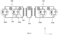
- FIG. 5 is a schematic that illustrates an example of a pair of coupled qubits 500, 502 in the same unit cell of a quantum computing processor.
- each qubit is a superconducting qubit and includes two parallel connected Josephson boxes 504a, 504b or 508a, 508b.
- Each Josephson box can include a Josephson junction 506 connected in parallel to a capacitor 507.
- each superconducting qubit is shown in FIG. 5 as having parallel connected Josephson boxes 504a, other arrangements are also possible. For example, in some example implementations, a single Josephson box can be used.
- the qubits 500, 502 are subject to an external transverse magnetic field B applied along a z direction perpendicular to the surface of the paper on which the figure is shown to give rise to the desired quantum effect (e.g., superposition); the B field is labeled by the symbol ⁇ .
- a set of inductive couplers 510 is placed between the qubits 500, 502 such that the qubits are coupled along the z-z directions in the space spanned by the operator basis (Pauli operators).
- the same arrangement shown in FIG. 5 can be used for a classical processor as well, with the exception that a transverse magnetic field is not applied to the nodes 500, 502 so that undesired quantum effects, such as superpositioning and quantum tunneling do not occur.
- the Hamiltonian of the quantum processor can be written as: where ⁇ i x and ⁇ i z are binary and each represents the spin of the i th qubit along the x direction or the z direction, respectively.
- h i and J ij are parameters that can be programmed for different problems to be solved by adjusting the inductive coupler set 508.
- h i and J ij have real values.
- N is the total number of logical qubits for computation.
- the sparsity of the parameter J ij is constrained by the hardware connectivity, i.e., the connectivity of the qubits shown in FIG. 5 . For unconnected qubits, the corresponding J ij is 0.
- I(t) and P(t) represent the time-dependency of initial and problem Hamiltonians, respectively.
- I(t) equals (1-s)
- P(t) equals s, where s equals t / t T , and t T is the total time for the annealing process.
- the quantum computing processor performs universal adiabatic quantum computations without being limited by 2-local stochastic Hamiltonians and can perform arbitrary or universal quantum operations in the adiabatic regime.
- the classical computing processor that is arranged on the same chip as the quantum computing processor can be configured to exchange data with the quantum computing processor by coupling the input and/or output of the active components of the classical processor to the input and/or output of the active components of the quantum processor.
- the processors can exchange information directly, e.g., by coupling superconducting flux bits to superconducting flux qubits.
- the resulting classical bits produced in the quantum processor by solving the optimization problem can be directly coupled to the classical processor.
- the state of one or more qubits from the quantum processor are projected to the classical computational basis.
- the output density operator of quantum processor is diagonal, which represents the classical mixture of computational basis capturing the statistical properties of quantum inference or quantum optimization protocol.
- the information can be transferred from the quantum processor to the classical processor through inductive coupling or via SWAP gates, with potential usage of repeaters to improve the fidelity of states. For instance, a 2-input/2-output SWAP gate simply exchanges the bit values it is provided.
- the classical processor then starts with the quantum-mechanically prepared ansatz and completes the computation fully classically. Direct coupling is possible, e.g., when there is a homogenous superconducting flux qubit/bit design throughout the chip (in both quantum and classical units), such as shown in FIGS. 4A-4B .
- FIG. 6 is a schematic that illustrates direct coupling between a quantum computing processor 604 and a classical computing processor 602.
- each processor includes 16 physical bits/qubits on two unit cells of 8 qubit/bit per unit within a Chimera graph.
- the intra-cell coupling 606a between hidden qubits/bits and data qubits/bits within a restricted layer will depend on the selected problem Hamiltonian).
- the coupling 606b represents mutual inductive coupling between hidden nodes of different unit cells.
- the coupling 606b is set to be ferromagnetic (+1) and simply copies the hidden nodes from one unit cell to another unit cell.
- the dashed line coupling 606c represent direct mutual inductive coupling between data nodes (input or output) of the quantum and classical processors.
- Coupling 606c becomes active at the end of or prior to the beginning of one or more iterations of the quantum processor to transfer data between the classical and quantum processors.
- the coupling 606c is during the computation phase of the quantum processor.
- Coupling 606c can be activated, for example, through the application of an appropriate external current to inductive couplers between the quantum and classical processors. Deactivation of the coupling 606c can be accomplished, for example, by withdrawing the external current from the inductive couplers between the quantum and classical processors.
- the processors can exchange information indirectly, e.g., where post-measurement processing is performed between transmission of data between the quantum and classical processor.
- the output of classical and quantum processors is post-processed at the end of each phase of computation and before being transferred to the other processor core.
- FIG. 7 is a schematic that illustrates indirect coupling between a quantum computing processor 704 and a classical computing processor 702.
- the arrangement of the processors is identical to the arrangement shown in FIG. 6 . That is, each processor includes 16 physical bits/qubits on two unit cells of 8 qubit/bit per unit within a Chimera graph. However, there are only four hidden and four input or output qubits/bits (denoted by "h,” “I,” and “O” respectively) within each unit cell. There are no interactions among hidden qubits/bits or among data (input or output) qubits/bits in each unit cell.
- the intra-cell coupling 706a between hidden qubits/bits and data qubits/bits within a restricted layer can be arbitrary (e.g., it depends on a given problem).
- the coupling 706b represents mutual inductive coupling between hidden nodes of different unit cells.
- the coupling 706b is set to be ferromagnetic (+1) and simply copies the hidden nodes from one unit cell to another unit cell.
- the dashed line coupling 706c represent indirect mutual inductive coupling between data nodes (input or output) of the quantum and classical processors.
- Coupling 706c still becomes active at the end of one or more iterations of the quantum processor (or at the end of one or more iterations of the classical processor) to transfer data between the classical and quantum processors, but the data being transferred now is modified by one or more processing elements 708, that can perform various data processing and analysis tasks, such as Bayesian analysis, signal amplification and/or error-correction. These tasks can be might be perform with additional superconducting components or CMOS-based processors.
- coupling 706c can be activated, for example, through the application of an appropriate external current to inductive couplers between the quantum and classical processors.
- Deactivation of the coupling 706c can be accomplished, for example, by withdrawing the external current from the inductive couplers between the quantum and classical processors.
- FIG. 8A is a schematic illustrating an example of direct coupling between a component 800 of a cell of a quantum computing processor and a component 802 of a classical computing processor.
- direct coupling is achieved through the use of mutual inductance through multiple inductive couplers 804 that are formed on the same chip as the quantum and classical processors.
- the data from the inductor of the component 800 (output qubit) is transferred to the inductor of the component 802 (input bit).
- the data from the inductor of the component 802 (output bit) is transferred to the inductor of the component 802 (input qubit).
- FIG. 8B is a schematic illustrating an example of indirect coupling between a component 800 of a cell of a quantum computing processor and a component 802 of a classical computing processor.
- Post-processing can include processing on additional bits/qubits at sub-Kelvin temperature or through traditional (e.g., CMOS-based) classical processors at that are operating at the room temperature.
- a substrate e.g., single crystal Si wafer
- the surface of the substrate can be oxidized to provide an insulating barrier.
- the layers of superconducting material are deposited and patterned on the substrate surface. For instance, a photoresist layer may be deposited and patterned first followed by deposition of the superconducting metals, after which a lift-off step is performed.
- the superconducting metal may be deposited and patterned using etching techniques (e.g., wet chemical etching).
- Oxides of the metals can be formed through standard techniques including for example, local oxidation of the superconducting metal.
- the patterning of the deposited metal and oxides can be designed to form the classical and quantum active and passive components, such as the Josephson junctions, capacitors and inductors, as well as the coupling connections between the processors.
- the devices can be operated at temperatures corresponding to the superconducting temperatures for the metals selected (e.g., less than 1 K) using, e.g., a dilution refrigerator.
- the classical computing processor 102 of the chip 100 can operate on data in combination with the quantum computing processor 104 to solve one or more problems.
- the state of qubits can be transferred to the classical processor.
- the classical processor could also return its output to the quantum solver as a new local initialization for another phase of quantum computation.
- the process can be done iteratively to converge to a steady state of overall dynamics assuming the overall dynamics of quantum and classical Markov chain is ergodic with a unique attracting state.
- the mixing time of the overall process could be shorter than fully quantum or fully classical algorithm for the same task.
- a classical bit string can be obtained by measuring populations of superconducting flux qubits of a quantum processor operating as a quantum annealer.
- a quantum annealer determines solutions to hard optimization problems by evolving a known initial configuration towards a ground state of a Hamiltonian that encodes an optimization problem.
- the state of the quantum devices within the processor evolve according to the laws of quantum mechanics and updates all variables simultaneously.
- the variable of a model can be mapped to the z-component of a quantum spin-half variable (qubit).
- a transverse magnetic field then is applied to induce quantum fluctuations, thus obtaining a time-dependent Hamiltonian.
- Quantum annealing at finite temperature T starts in the limit of a strong transverse field and weak couplings. Decreasing the strength of the transverse field increases the couplings and allows the system to evolve towards the ground state of the optimization problem.
- the output states of the quantum annealer then can be fed into thermal/classical annealer (which has the same superconducting flux components but operating in their corresponding classical limit, e.g., without application of the transverse magnetic field).
- the output of classical processor (which would be another bit string correspond to combinatory values of bits being either 0 or 1) can be fed back into quantum annealer as a seed solution.
- the above strategy can provide a better time-to-solution with a given desired residual energy (accuracy of solution) than fully quantum or fully classical strategies.
- the combined provides better energy efficiency and robustness by performing both classical and quantum computation at a superconducting phase at the same sub-Kelvin temperature scale.
- FIG. 9 is a plot that shows a generic example of a non-convex objective function versus state space, in which quantum and classical processors on a combined chip can perform mixed quantum annealing and simulated annealing to obtain the desired residual energy.
- Classical simulated annealing performs well when thermal jumps/hops occur over short energy barrier (arrows 902).
- quantum annealing performs better when energy barrier are tall and narrow such that tunneling can occur (arrows 904).
- the combined chip can perform better than either of quantum or classical processors alone to sample the objective function that exhibits both tall-narrow energy barriers as well as short energy barriers.
- cross hairs corresponds to an output bit string of a quantum (906) or classical (908) processor.
- the system can quickly reach the desired residual energy and a more accurate solution (e.g., global minimum of the objective function as opposed to a less accurate local minimum).
- a more accurate solution e.g., global minimum of the objective function as opposed to a less accurate local minimum.
- the classical and quantum processors may be configured to implement a model, such as an artificial neural network model.
- Artificial neural networks are useful systems for solving complex problems (e.g., machine learning problems such as classification problems, pattern matching problems, image recognition problems, speech recognition problems, voice recognition problems, or object recognition problems), in which the network represents a trained model, e.g., a trained undirected graphical model.
- the model is trained by inputting training data to the model, i.e., initial model parameters are determined from training data.
- the refinement of the model parameters may occur as additional data, whether training data or observable data, is fed into the model.
- Certain steps in the training of the model or when using the model for predictions may be performed using the quantum computing processor 104.
- the classical computing processor 102 may implement the model and provide an output of the model to the quantum computing processor 104 to address a separate problem for which the quantum computing processor is designed.
- FIG. 10 is a graphical representation of an example feed-forward neural network model 1100.
- a feed-forward neural network model is a basic type of artificial neural network model in which information always moves in one direction.
- the network model 1100 is represented as a network of nodes 1108, 1110, 1112, 1114, 1116, 1118, 1120, 1122, 1124 arranged in layers, 1102, 1104, and 1106, where information moves from input layer 1102 to output layer 1106.
- Each node is connected with at least one other node through a connection 1126.
- Each node is also defined with an energy and is stochastic, whereas each connection 1120 can be a parameter that represents the connection strength between the two nodes.
- the nodes within the same layer do not interact with each other, and the nodes within different layers interact with each other.
- the layers may be visible or invisible.
- a visible layer is one which receives input data from or provides output data to a source external to the model, whereas an invisible layer receives input from or provides output to another layer in the model.
- the variables in the visible layers 1102, 1106 are denoted as x, y, respectively.
- the variables x are the input, which will receive observed data, after the model is trained, and the variables y are the output.
- the variables in the hidden layer are labeled as s. In the example shown in the figure, the hidden nodes have interactions with each other and the visible nodes have interactions among themselves.
- a neural network model such as model 1100
- parameters of the model are determined with the goal that the trained model optimally fits the observed data from any of the problems to be solved.
- Part of or the entire training of the model can be computationally intractable, depending on the size or complexity of the model, or both.
- the time the model must be trained in order to collect equilibrium statistics can grow exponentially with the size (e.g., number of parameters or units in a network) of the model.
- a quantum computing processor can be used to train the model, such as model 1100, and provide the solution as an output at layer 1106.
- the output at layer 1106 then can be coupled to the classical processor for further processing of the results.
- the classical processor can provide a classical input as a "seed" to layer 1102 of the model 1100, where the quantum processor subsequently trains the seeded model.
- the quantum and classical computing processors require ultra-cold operating temperature to allow certain materials within the processors to achieve superconductivity.
- the ultra-cold temperatures can be provided by a cryogenic refrigeration subsystem.
- Various systems and methods exist for producing and sustaining cryogenic temperatures. Examples of such systems include liquid cryogenic baths (e.g., liquid nitrogen or liquid helium), Stirling cryocoolers, Joule-Thomson cryocoolers, adsorption refrigerators, dilution refrigerators, adiabatic demagnetization refrigerators, among others.
- superconducting shielding can be provided to reduce the strength of interference such as magnetic and electrical fields.
- FIG. 11 is a schematic that illustrates an example of a system 1200 for performing quantum and/or classical computing operations using the combined quantum and classical processor on the same chip as described herein.
- the system 1200 includes a chip 1202 on which are formed a classical computing processor and a quantum computing processor.
- the data inputs/outputs of the quantum computing processor and classical computing processor are accessible to one another through one or more couplers formed on the same chip 1202.
- the chip 1202 is cooled to an ultra-cold temperature suitable for allowing materials on the chip 1202 to obtain superconductivity using a refrigeration system 1204.
- the chip 1202 also is coupled to a separate data storage device 1206 having computer readable media suitable for storing computer readable instructions and data including one or more forms of nonvolatile memory, media and memory devices, including by way of example semiconductor memory devices, e.g., EPROM, EEPROM, and flash memory devices; magnetic disks, e.g., internal hard disks or removable disks; magneto optical disks; and CD ROM and DVD-ROM disks.
- semiconductor memory devices e.g., EPROM, EEPROM, and flash memory devices
- magnetic disks e.g., internal hard disks or removable disks
- magneto optical disks e.g., CD ROM and DVD-ROM disks
- CD ROM and DVD-ROM disks CD ROM and DVD-ROM disks.
- one or more inputs and/or outputs of the classical processor on the chip 1202 can be coupled to the data storage device 1206 for transmitting data to and/or receiving data from the data storage device 1206.
- the system 1200 can include a user interface device 1208, e.g., a CRT cathode ray tube or LCD (liquid crystal display) monitor, for displaying information to the user and a keyboard and a pointing device, e.g., a mouse or a trackball, by which the user can provide input to the computer.
- a user interface device 1208 can be coupled to the chip 1202 through a classical data processing apparatus that, in some cases, includes the data storage device 1206.
- a classical data processing apparatus can include, for example, a CMOS-based computer system.
Landscapes
- Engineering & Computer Science (AREA)
- Theoretical Computer Science (AREA)
- Physics & Mathematics (AREA)
- General Physics & Mathematics (AREA)
- General Engineering & Computer Science (AREA)
- Computing Systems (AREA)
- Mathematical Physics (AREA)
- Computer Hardware Design (AREA)
- Artificial Intelligence (AREA)
- Computational Mathematics (AREA)
- Condensed Matter Physics & Semiconductors (AREA)
- Data Mining & Analysis (AREA)
- Evolutionary Computation (AREA)
- Mathematical Analysis (AREA)
- Mathematical Optimization (AREA)
- Pure & Applied Mathematics (AREA)
- Software Systems (AREA)
- Superconductor Devices And Manufacturing Methods Thereof (AREA)
- Logic Circuits (AREA)
Claims (13)
- Appareil comprenant :une puce ;un processeur informatique classique formé sur la puce ;un processeur informatique quantique formé sur la puce ;la puce étant une puce unique de sorte que le processeur informatique classique et le processeur informatique quantique sont mis en œuvre à l'aide de la puce unique ; etun ou plusieurs composants d'accouplement inductifs entre le processeur informatique classique et le processeur informatique quantique, les un ou plusieurs composants d'accouplement inductifs étant formés sur la puce et étant configurés pour permettre l'échange de données entre le processeur informatique classique et le processeur informatique quantique ;dans lequel le processeur informatique classique comprend une pluralité de cellules d'unité classique, chaque cellule d'unité classique comprenant une pluralité de composants actifs configurés pour générer un bit classique respectif, dans lequel, pour chaque cellule d'unité classique, un premier sous-ensemble de la pluralité de composants actifs est couplé à un second sous-ensemble de la pluralité de composants actifs ;dans lequel le processeur informatique quantique comprend une pluralité de cellules d'unité quantique comprenant une pluralité respective de qubits dans lequel, pour chaque cellule d'unité quantique, un premier sous-ensemble de la pluralité de qubits est couplé à un second sous-ensemble de la pluralité de qubits ;dans lequel, pour chaque cellule d'unité classique, le premier sous-ensemble de la pluralité de composants actifs est couplé, par les un ou plusieurs composants d'accouplement inductifs, au premier sous-ensemble de qubits dans une cellule d'unité quantique correspondante ;dans lequel :le premier sous-ensemble de la pluralité de qubits fournit une entrée au processeur informatique quantique et une sortie depuis celui-ci, dans lequel les qubits qui fournissent l'entrée ne fournissent pas la sortie ;une sortie du processeur informatique classique est couplée à l'entrée du processeur informatique quantique ;la sortie du processeur informatique quantique est couplée à une entrée du processeur informatique classique ; etle second sous-ensemble de la pluralité de qubits n'est pas couplé au processeur informatique classique.
- Appareil selon la revendication 1, dans lequel le processeur informatique quantique est configuré pour recevoir des données de sortie depuis le processeur informatique classique et utiliser les données de sortie reçues en tant que données d'entrée pour un calcul quantique à exécuter par le processeur informatique quantique.
- Appareil selon la revendication 2, dans lequel le processeur informatique quantique est configuré pour être programmé à l'aide des données de sortie.
- Appareil selon la revendication 1, dans lequel chacun du processeur informatique quantique et du processeur informatique classique comprend un dispositif supraconducteur à interférence quantique (SQUID).
- Appareil selon la revendication 1, dans lequel chacun du processeur informatique quantique et du processeur informatique classique comprend au moins une jonction Josephson et une bobine d'induction.
- Appareil selon la revendication 1, dans lequel les un ou plusieurs composants d'accouplement inductifs comprennent un fil supraconducteur.
- Appareil selon la revendication 1, dans lequel le processeur informatique classique comprend une pluralité de portes logiques quantiques agencées selon une logique quantique réciproque (RQL).
- Appareil selon la revendication 1, dans lequel chacun du processeur informatique quantique et du processeur informatique classique comprend un matériau supraconducteur.
- Appareil selon la revendication 8, dans lequel le matériau supraconducteur comprend de l'aluminium, du niobium ou un alliage de plomb.
- Appareil selon la revendication 1, dans lequel l'un ou plusieurs composants d'accouplement inductif comprennent un ensemble de lignes de transmission par électrodynamique quantique (QED) en cavité supraconductrices.
- Appareil selon l'une quelconque des revendications précédentes, dans lequel, pour chaque cellule d'unité classique, le second sous-ensemble de composants actifs est couplé à un sous-ensemble de composants actifs d'une autre cellule d'unité classique, et pour chaque cellule quantique, le second sous-ensemble de qubits est couplé à un sous-ensemble de qubits d'une autre cellule d'unité quantique.
- Appareil selon la revendication 11, dans lequel, pour chaque cellule d'unité quantique, le second sous-ensemble de qubits est couplé au sous-ensemble de qubits d'une autre cellule d'unité quantique par un couplage ferromagnétique.
- Système comprenant :un appareil selon la revendication 1 ; etun dispositif de stockage de mémoire accessible par l'appareil.
Applications Claiming Priority (2)
| Application Number | Priority Date | Filing Date | Title |
|---|---|---|---|
| US201461968993P | 2014-03-21 | 2014-03-21 | |
| PCT/US2015/022035 WO2015143439A1 (fr) | 2014-03-21 | 2015-03-23 | Puces comprenant des processeurs informatiques classique et quantique |
Publications (3)
| Publication Number | Publication Date |
|---|---|
| EP3120460A1 EP3120460A1 (fr) | 2017-01-25 |
| EP3120460A4 EP3120460A4 (fr) | 2017-11-22 |
| EP3120460B1 true EP3120460B1 (fr) | 2020-10-14 |
Family
ID=54145424
Family Applications (1)
| Application Number | Title | Priority Date | Filing Date |
|---|---|---|---|
| EP15765127.4A Active EP3120460B1 (fr) | 2014-03-21 | 2015-03-23 | Puces comprenant des processeurs informatiques classique et quantique |
Country Status (5)
| Country | Link |
|---|---|
| US (3) | US10671559B2 (fr) |
| EP (1) | EP3120460B1 (fr) |
| AU (1) | AU2015230964B2 (fr) |
| CA (1) | CA2943489C (fr) |
| WO (1) | WO2015143439A1 (fr) |
Cited By (1)
| Publication number | Priority date | Publication date | Assignee | Title |
|---|---|---|---|---|
| US12481864B2 (en) | 2022-06-16 | 2025-11-25 | International Business Machines Corporation | Generating hybrid quantum-classical neural network architectures |
Families Citing this family (71)
| Publication number | Priority date | Publication date | Assignee | Title |
|---|---|---|---|---|
| US9471880B2 (en) * | 2013-04-12 | 2016-10-18 | D-Wave Systems Inc. | Systems and methods for interacting with a quantum computing system |
| US10127499B1 (en) | 2014-08-11 | 2018-11-13 | Rigetti & Co, Inc. | Operating a quantum processor in a heterogeneous computing architecture |
| US10097182B2 (en) | 2014-12-31 | 2018-10-09 | Stmicroelectronics, Inc. | Integrated circuit layout wiring for multi-core chips |
| US10102327B2 (en) | 2014-12-31 | 2018-10-16 | Stmicroelectronics, Inc. | Integrated circuit layout wiring for multi-core chips |
| US10187814B2 (en) | 2015-05-14 | 2019-01-22 | Cable Television Laboratories, Inc. | Systems and methods for hybrid wireless communication network |
| US11647407B1 (en) * | 2015-05-14 | 2023-05-09 | Cable Television Laboratories, Inc. | Systems and methods for hybrid quantum wireless communication network |
| CA3162818C (fr) | 2015-09-30 | 2025-11-18 | Google Llc | Qubits de flux de guide d’ondes coplanaire |
| US10140404B2 (en) | 2015-11-06 | 2018-11-27 | Rigetti & Co, Inc. | Analyzing quantum information processing circuits |
| US10275718B2 (en) * | 2015-11-17 | 2019-04-30 | Massachusetts Institute Of Technology | Paramagnetic tree coupling of spin qubits |
| US10187065B2 (en) | 2015-11-17 | 2019-01-22 | Massachusetts Institute Of Technology | Four spin couplers for quantum information processing |
| WO2017087627A1 (fr) | 2015-11-17 | 2017-05-26 | Massachusetts Institute Of Technology | Interféromètres à boucles multiples de traitement d'informations quantiques |
| WO2017117016A1 (fr) * | 2015-12-30 | 2017-07-06 | Google Inc. | Amélioration de recuit simulé avec recuit quantique |
| US10599988B2 (en) | 2016-03-02 | 2020-03-24 | D-Wave Systems Inc. | Systems and methods for analog processing of problem graphs having arbitrary size and/or connectivity |
| WO2017155531A1 (fr) * | 2016-03-10 | 2017-09-14 | Technische Universiteit Delft | Trous d'interconnexion hyperfréquence supraconducteurs pour circuits quantiques multiplanaires |
| US10325218B1 (en) * | 2016-03-10 | 2019-06-18 | Rigetti & Co, Inc. | Constructing quantum process for quantum processors |
| US10229355B2 (en) | 2016-04-13 | 2019-03-12 | Iqb Information Technologies Inc. | Quantum processor and its use for implementing a neural network |
| CA3022037C (fr) | 2016-04-25 | 2021-09-21 | Google Llc | Optimisation assistee par quantum |
| US10671937B2 (en) | 2016-06-08 | 2020-06-02 | D-Wave Systems Inc. | Systems and methods for quantum computation |
| US10050630B2 (en) * | 2016-08-19 | 2018-08-14 | Rigetti & Co, Inc. | Flux-tunable qubit device with multiple Josephson junctions |
| WO2018057024A1 (fr) * | 2016-09-26 | 2018-03-29 | Intel Corporation | Échangeur de chaleur en argent fritté pour bits quantiques |
| EP3520139A4 (fr) * | 2016-09-29 | 2020-04-22 | INTEL Corporation | Assemblages de calculateurs quantiques |
| EP3520041B1 (fr) * | 2016-09-30 | 2026-03-11 | Rigetti & Co, LLC | Simulation de systèmes quantiques avec calcul quantique |
| US10346508B2 (en) | 2017-01-12 | 2019-07-09 | D-Wave Systems Inc. | Re-equilibrated quantum sampling |
| US11263547B2 (en) | 2017-01-30 | 2022-03-01 | D-Wave Systems Inc. | Quantum annealing debugging systems and methods |
| US10270594B2 (en) * | 2017-03-06 | 2019-04-23 | Bank Of America Corporation | Enhanced polymorphic quantum enabled firewall |
| US11120356B2 (en) * | 2017-03-17 | 2021-09-14 | Bank Of America Corporation | Morphing federated model for real-time prevention of resource abuse |
| US10977570B2 (en) * | 2017-06-19 | 2021-04-13 | Rigetti & Co, Inc. | Distributed quantum computing system |
| US10380494B2 (en) * | 2017-08-04 | 2019-08-13 | International Business Machines Corporation | Josephson junctions for improved qubits |
| US11250341B2 (en) | 2017-09-07 | 2022-02-15 | Lockheed Martin Corporation | System, method and computer readable medium for quassical computing |
| WO2019059879A1 (fr) * | 2017-09-19 | 2019-03-28 | Google Llc | Piliers en tant que butées pour une séparation précise de puce à puce |
| US10355193B2 (en) * | 2017-11-28 | 2019-07-16 | International Business Machines Corporation | Flip chip integration on qubit chips |
| US10340438B2 (en) | 2017-11-28 | 2019-07-02 | International Business Machines Corporation | Laser annealing qubits for optimized frequency allocation |
| US11895931B2 (en) * | 2017-11-28 | 2024-02-06 | International Business Machines Corporation | Frequency tuning of multi-qubit systems |
| US10170681B1 (en) | 2017-11-28 | 2019-01-01 | International Business Machines Corporation | Laser annealing of qubits with structured illumination |
| US10418540B2 (en) | 2017-11-28 | 2019-09-17 | International Business Machines Corporation | Adjustment of qubit frequency through annealing |
| WO2019133889A1 (fr) | 2017-12-29 | 2019-07-04 | Google Llc | Programmes de recuit quantique non homogène |
| US11010145B1 (en) | 2018-02-21 | 2021-05-18 | Rigetti & Co, Inc. | Retargetable compilation for quantum computing systems |
| US11100418B2 (en) | 2018-02-28 | 2021-08-24 | D-Wave Systems Inc. | Error reduction and, or, correction in analog computing including quantum processor-based computing |
| US11481354B2 (en) | 2018-04-24 | 2022-10-25 | D-Wave Systems Inc. | Systems and methods for calculating the ground state of non-diagonal Hamiltonians |
| US11308248B2 (en) * | 2018-05-05 | 2022-04-19 | Intel Corporation | Apparatus and method for quantum computing performance simulation |
| US11551127B1 (en) | 2018-05-09 | 2023-01-10 | Rigetti & Co, Llc | Using a quantum processor unit to preprocess data |
| WO2019222748A1 (fr) | 2018-05-18 | 2019-11-21 | Rigetti & Co, Inc. | Plateforme de calcul à processeurs quantiques hétérogènes |
| WO2020033807A1 (fr) | 2018-08-09 | 2020-02-13 | Rigetti & Co, Inc. | Noyau quantique de diffusion en continu |
| US11121302B2 (en) | 2018-10-11 | 2021-09-14 | SeeQC, Inc. | System and method for superconducting multi-chip module |
| US11593174B2 (en) | 2018-10-16 | 2023-02-28 | D-Wave Systems Inc. | Systems and methods for scheduling programs for dedicated execution on a quantum processor |
| US10891251B2 (en) | 2018-11-09 | 2021-01-12 | International Business Machines Corporation | Signal connector for microwave circuits |
| US11501196B2 (en) * | 2018-11-26 | 2022-11-15 | International Business Machines Corporation | Qubit tuning by magnetic fields in superconductors |
| CN113544711B (zh) | 2019-01-17 | 2024-08-02 | D-波系统公司 | 用于使用聚类收缩的混合算法系统和方法 |
| US11900264B2 (en) | 2019-02-08 | 2024-02-13 | D-Wave Systems Inc. | Systems and methods for hybrid quantum-classical computing |
| WO2020168158A1 (fr) * | 2019-02-15 | 2020-08-20 | Rigetti & Co, Inc. | Synthèse automatisée de programmes quantiques |
| US11551125B2 (en) * | 2019-02-21 | 2023-01-10 | International Business Machines Corporation | High density microwave hermetic interconnects for quantum applications |
| US11567779B2 (en) | 2019-03-13 | 2023-01-31 | D-Wave Systems Inc. | Systems and methods for simulation of dynamic systems |
| US11593695B2 (en) | 2019-03-26 | 2023-02-28 | D-Wave Systems Inc. | Systems and methods for hybrid analog and digital processing of a computational problem using mean fields |
| US11088310B2 (en) | 2019-04-29 | 2021-08-10 | International Business Machines Corporation | Through-silicon-via fabrication in planar quantum devices |
| US12387130B1 (en) | 2019-08-08 | 2025-08-12 | Rigetti & Co, Llc | Automated synthesizing and compilation of quantum programs |
| US11714730B2 (en) | 2019-08-20 | 2023-08-01 | D-Wave Systems Inc. | Systems and methods for high availability, failover and load balancing of heterogeneous resources |
| US10817463B1 (en) * | 2019-09-30 | 2020-10-27 | Zettaflops Llc | Adiabatic circuits for cold scalable electronics |
| CA3189506A1 (fr) * | 2020-06-03 | 2021-12-09 | SeeQC Inc. | Materiels et procedes pour la fabrication de circuits integres quantiques supraconducteurs |
| US12293253B2 (en) * | 2020-08-19 | 2025-05-06 | International Business Machines Corporation | Multipole filter on a quantum device with multiplexing and signal separation |
| US11676058B2 (en) * | 2020-09-03 | 2023-06-13 | Graham MOREHEAD | System and method for artificial intelligence |
| US12106178B2 (en) | 2020-09-11 | 2024-10-01 | International Business Machines Corporation | Quantum state measurement logic facilitating a quantum state measurement backend process |
| US12242924B2 (en) | 2020-09-11 | 2025-03-04 | International Business Machines Corporation | Mapping conditional execution logic to quantum computing resources |
| US11567887B2 (en) | 2020-09-11 | 2023-01-31 | International Business Machines Corporation | Quantum controller fast path interface |
| CN112349330B (zh) * | 2020-11-03 | 2023-11-21 | 中国科学院计算技术研究所 | 一种sfq电路与cmos电路间交互方法及系统 |
| US11853848B2 (en) * | 2021-05-07 | 2023-12-26 | International Business Machines Corporation | Backend quantum runtimes |
| JP2024526085A (ja) | 2021-06-11 | 2024-07-17 | シーク, インコーポレイテッド | 超伝導量子回路のための磁束バイアスのシステム及び方法 |
| US11948046B2 (en) | 2022-05-25 | 2024-04-02 | Red Hat, Inc. | MVC inspired quantum-classical service |
| US12488267B2 (en) * | 2022-07-01 | 2025-12-02 | University Of Tartu | Shift rule for gradient determination in parameterised quantum evolutions |
| DE102022208639A1 (de) * | 2022-08-19 | 2024-02-22 | Siemens Aktiengesellschaft | Quantenrechner für eine hybride quanten-klassische Informationsverarbeitung mit einem Schaltungsträger |
| WO2024037917A1 (fr) * | 2022-08-19 | 2024-02-22 | Siemens Aktiengesellschaft | Ordinateur quantique pour traitement d'informations hybride quantique-classique avec support de circuit |
| US20240386031A1 (en) * | 2023-05-17 | 2024-11-21 | Bank Of America Corporation | Real-time data modeling for data warehouse using quantum computing |
Family Cites Families (21)
| Publication number | Priority date | Publication date | Assignee | Title |
|---|---|---|---|---|
| JP2822773B2 (ja) * | 1992-04-28 | 1998-11-11 | 住友電気工業株式会社 | 超電導インタフェース回路 |
| NO308149B1 (no) * | 1998-06-02 | 2000-07-31 | Thin Film Electronics Asa | Skalerbar, integrert databehandlingsinnretning |
| GB9916209D0 (en) * | 1999-07-09 | 1999-09-15 | Isis Innovation | Data processor |
| US7418283B2 (en) * | 2004-03-29 | 2008-08-26 | D-Wave Systems Inc. | Adiabatic quantum computation with superconducting qubits |
| US20070239366A1 (en) * | 2004-06-05 | 2007-10-11 | Hilton Jeremy P | Hybrid classical-quantum computer architecture for molecular modeling |
| US8983303B2 (en) * | 2004-08-04 | 2015-03-17 | The United States Of America As Represented By The Secretary Of The Army | Quantum based information transfer system and method |
| US7875876B1 (en) * | 2006-06-15 | 2011-01-25 | Hrl Laboratories, Llc | Scalable quantum computer |
| US8098179B2 (en) * | 2007-05-14 | 2012-01-17 | D-Wave Systems Inc. | Systems, methods and apparatus for digital-to-analog conversion of superconducting magnetic flux signals |
| US7893708B2 (en) * | 2007-08-03 | 2011-02-22 | Northrop Grumman Systems Corporation | Quantum gate operations with a common coupled resonator |
| US8670807B2 (en) * | 2007-08-21 | 2014-03-11 | D-Wave Systems Inc. | Systems, methods, and apparatus for controlling the elements of superconducting processors |
| US8190548B2 (en) * | 2007-11-08 | 2012-05-29 | D-Wave Systems Inc. | Systems, devices, and methods for analog processing |
| US7969178B2 (en) * | 2008-05-29 | 2011-06-28 | Northrop Grumman Systems Corporation | Method and apparatus for controlling qubits with single flux quantum logic |
| EP3098865B1 (fr) * | 2009-02-27 | 2018-10-03 | D-Wave Systems Inc. | Procédé de fabrication d'un circuit intégré supraconducteur |
| GB201013721D0 (en) * | 2010-08-16 | 2010-09-29 | Mbda Uk Ltd | Image processing method |
| US8338294B2 (en) * | 2011-03-31 | 2012-12-25 | Soitec | Methods of forming bonded semiconductor structures including two or more processed semiconductor structures carried by a common substrate, and semiconductor structures formed by such methods |
| US8508280B2 (en) * | 2011-07-11 | 2013-08-13 | Northrop Grumman Systems Corporation | Qubit readout via resonant scattering of josephson solitons |
| US9768371B2 (en) * | 2012-03-08 | 2017-09-19 | D-Wave Systems Inc. | Systems and methods for fabrication of superconducting integrated circuits |
| US9178154B2 (en) * | 2012-10-09 | 2015-11-03 | D-Wave Systems Inc. | Quantum processor comprising a second set of inter-cell coupling devices where a respective pair of qubits in proximity adjacent unit cells crossed one another |
| US9530873B1 (en) * | 2013-01-28 | 2016-12-27 | Sandia Corporation | Semiconductor adiabatic qubits |
| US9183508B2 (en) * | 2013-08-07 | 2015-11-10 | D-Wave Systems Inc. | Systems and devices for quantum processor architectures |
| US9520180B1 (en) * | 2014-03-11 | 2016-12-13 | Hypres, Inc. | System and method for cryogenic hybrid technology computing and memory |
-
2015
- 2015-03-23 EP EP15765127.4A patent/EP3120460B1/fr active Active
- 2015-03-23 WO PCT/US2015/022035 patent/WO2015143439A1/fr not_active Ceased
- 2015-03-23 US US15/127,695 patent/US10671559B2/en active Active
- 2015-03-23 CA CA2943489A patent/CA2943489C/fr active Active
- 2015-03-23 AU AU2015230964A patent/AU2015230964B2/en active Active
-
2020
- 2020-04-30 US US16/863,623 patent/US11238000B2/en active Active
-
2022
- 2022-01-13 US US17/575,552 patent/US12086091B2/en active Active
Non-Patent Citations (1)
| Title |
|---|
| None * |
Cited By (1)
| Publication number | Priority date | Publication date | Assignee | Title |
|---|---|---|---|---|
| US12481864B2 (en) | 2022-06-16 | 2025-11-25 | International Business Machines Corporation | Generating hybrid quantum-classical neural network architectures |
Also Published As
| Publication number | Publication date |
|---|---|
| US11238000B2 (en) | 2022-02-01 |
| US12086091B2 (en) | 2024-09-10 |
| CA2943489A1 (fr) | 2015-09-24 |
| EP3120460A4 (fr) | 2017-11-22 |
| CA2943489C (fr) | 2019-11-12 |
| US20200257644A1 (en) | 2020-08-13 |
| US20170177534A1 (en) | 2017-06-22 |
| AU2015230964A1 (en) | 2016-10-06 |
| US20220214991A1 (en) | 2022-07-07 |
| WO2015143439A1 (fr) | 2015-09-24 |
| EP3120460A1 (fr) | 2017-01-25 |
| US10671559B2 (en) | 2020-06-02 |
| AU2015230964B2 (en) | 2018-05-24 |
Similar Documents
| Publication | Publication Date | Title |
|---|---|---|
| US12086091B2 (en) | Chips including classical and quantum computing processors | |
| Schneider et al. | Tutorial: High-speed low-power neuromorphic systems based on magnetic Josephson junctions | |
| CN101548288B (zh) | 用于量子处理器元件本地编程的系统、方法和装置 | |
| Steffen et al. | Quantum computing: An IBM perspective | |
| US7932515B2 (en) | Quantum processor | |
| US7898282B2 (en) | Systems, devices, and methods for controllably coupling qubits | |
| AU2006255515B2 (en) | Qubit state copying | |
| US9369133B2 (en) | Hybrid quantum circuit assembly | |
| Holmes et al. | Superconducting computing in large-scale hybrid systems | |
| US20240020562A1 (en) | Quantum computing systems with diabatic single flux quantum (sfq) readout for superconducting quantum bits | |
| CN113939833A (zh) | 单线量子位控制 | |
| Schegolev et al. | Superconducting Neural Networks: from an Idea to Fundamentals and, further, to Application | |
| Holmes | Cryogenic electronics and quantum information processing | |
| Keçeci | Investigating Layered Structures Containing Weyl and Majorana Fermions via the Stratum Model | |
| CN110709934A (zh) | 超导装置中的磁通量控制 | |
| Halder et al. | Introduction: Superconducting Qubits and Their Realizations | |
| WO2025058661A9 (fr) | Systèmes et procédés de champ de lecture d'état de bit quantique | |
| Wong | Review of Superconducting Qubit Devices and Their Large-Scale Integration |
Legal Events
| Date | Code | Title | Description |
|---|---|---|---|
| STAA | Information on the status of an ep patent application or granted ep patent |
Free format text: STATUS: THE INTERNATIONAL PUBLICATION HAS BEEN MADE |
|
| PUAI | Public reference made under article 153(3) epc to a published international application that has entered the european phase |
Free format text: ORIGINAL CODE: 0009012 |
|
| STAA | Information on the status of an ep patent application or granted ep patent |
Free format text: STATUS: REQUEST FOR EXAMINATION WAS MADE |
|
| 17P | Request for examination filed |
Effective date: 20160921 |
|
| AK | Designated contracting states |
Kind code of ref document: A1 Designated state(s): AL AT BE BG CH CY CZ DE DK EE ES FI FR GB GR HR HU IE IS IT LI LT LU LV MC MK MT NL NO PL PT RO RS SE SI SK SM TR |
|
| AX | Request for extension of the european patent |
Extension state: BA ME |
|
| DAV | Request for validation of the european patent (deleted) | ||
| DAX | Request for extension of the european patent (deleted) | ||
| RAP1 | Party data changed (applicant data changed or rights of an application transferred) |
Owner name: GOOGLE LLC |
|
| A4 | Supplementary search report drawn up and despatched |
Effective date: 20171024 |
|
| RIC1 | Information provided on ipc code assigned before grant |
Ipc: H01L 27/18 20060101ALI20171018BHEP Ipc: H01L 39/22 20060101ALI20171018BHEP Ipc: H03K 19/195 20060101AFI20171018BHEP Ipc: G06N 99/00 20100101ALI20171018BHEP Ipc: G06F 13/40 20060101ALI20171018BHEP |
|
| STAA | Information on the status of an ep patent application or granted ep patent |
Free format text: STATUS: EXAMINATION IS IN PROGRESS |
|
| 17Q | First examination report despatched |
Effective date: 20190325 |
|
| REG | Reference to a national code |
Ref country code: DE Ref legal event code: R079 Ref document number: 602015060462 Country of ref document: DE Free format text: PREVIOUS MAIN CLASS: H03K0019195000 Ipc: G06N0010000000 |
|
| GRAP | Despatch of communication of intention to grant a patent |
Free format text: ORIGINAL CODE: EPIDOSNIGR1 |
|
| STAA | Information on the status of an ep patent application or granted ep patent |
Free format text: STATUS: GRANT OF PATENT IS INTENDED |
|
| RIC1 | Information provided on ipc code assigned before grant |
Ipc: G06N 10/00 20190101AFI20200511BHEP Ipc: H01L 27/18 20060101ALI20200511BHEP Ipc: H01L 39/22 20060101ALI20200511BHEP Ipc: H03K 19/195 20060101ALI20200511BHEP Ipc: G06F 13/40 20060101ALI20200511BHEP |
|
| INTG | Intention to grant announced |
Effective date: 20200604 |
|
| GRAS | Grant fee paid |
Free format text: ORIGINAL CODE: EPIDOSNIGR3 |
|
| GRAA | (expected) grant |
Free format text: ORIGINAL CODE: 0009210 |
|
| STAA | Information on the status of an ep patent application or granted ep patent |
Free format text: STATUS: THE PATENT HAS BEEN GRANTED |
|
| AK | Designated contracting states |
Kind code of ref document: B1 Designated state(s): AL AT BE BG CH CY CZ DE DK EE ES FI FR GB GR HR HU IE IS IT LI LT LU LV MC MK MT NL NO PL PT RO RS SE SI SK SM TR |
|
| REG | Reference to a national code |
Ref country code: GB Ref legal event code: FG4D |
|
| REG | Reference to a national code |
Ref country code: AT Ref legal event code: REF Ref document number: 1324313 Country of ref document: AT Kind code of ref document: T Effective date: 20201015 Ref country code: CH Ref legal event code: EP |
|
| REG | Reference to a national code |
Ref country code: DE Ref legal event code: R082 Ref document number: 602015060462 Country of ref document: DE Representative=s name: VENNER SHIPLEY GERMANY LLP, DE Ref country code: DE Ref legal event code: R082 Ref document number: 602015060462 Country of ref document: DE Representative=s name: VENNER SHIPLEY LLP, DE |
|
| REG | Reference to a national code |
Ref country code: DE Ref legal event code: R096 Ref document number: 602015060462 Country of ref document: DE |
|
| REG | Reference to a national code |
Ref country code: IE Ref legal event code: FG4D |
|
| REG | Reference to a national code |
Ref country code: AT Ref legal event code: MK05 Ref document number: 1324313 Country of ref document: AT Kind code of ref document: T Effective date: 20201014 |
|
| REG | Reference to a national code |
Ref country code: NL Ref legal event code: MP Effective date: 20201014 |
|
| PG25 | Lapsed in a contracting state [announced via postgrant information from national office to epo] |
Ref country code: NL Free format text: LAPSE BECAUSE OF FAILURE TO SUBMIT A TRANSLATION OF THE DESCRIPTION OR TO PAY THE FEE WITHIN THE PRESCRIBED TIME-LIMIT Effective date: 20201014 Ref country code: NO Free format text: LAPSE BECAUSE OF FAILURE TO SUBMIT A TRANSLATION OF THE DESCRIPTION OR TO PAY THE FEE WITHIN THE PRESCRIBED TIME-LIMIT Effective date: 20210114 Ref country code: PT Free format text: LAPSE BECAUSE OF FAILURE TO SUBMIT A TRANSLATION OF THE DESCRIPTION OR TO PAY THE FEE WITHIN THE PRESCRIBED TIME-LIMIT Effective date: 20210215 Ref country code: RS Free format text: LAPSE BECAUSE OF FAILURE TO SUBMIT A TRANSLATION OF THE DESCRIPTION OR TO PAY THE FEE WITHIN THE PRESCRIBED TIME-LIMIT Effective date: 20201014 Ref country code: FI Free format text: LAPSE BECAUSE OF FAILURE TO SUBMIT A TRANSLATION OF THE DESCRIPTION OR TO PAY THE FEE WITHIN THE PRESCRIBED TIME-LIMIT Effective date: 20201014 Ref country code: GR Free format text: LAPSE BECAUSE OF FAILURE TO SUBMIT A TRANSLATION OF THE DESCRIPTION OR TO PAY THE FEE WITHIN THE PRESCRIBED TIME-LIMIT Effective date: 20210115 |
|
| REG | Reference to a national code |
Ref country code: LT Ref legal event code: MG4D |
|
| PG25 | Lapsed in a contracting state [announced via postgrant information from national office to epo] |
Ref country code: SE Free format text: LAPSE BECAUSE OF FAILURE TO SUBMIT A TRANSLATION OF THE DESCRIPTION OR TO PAY THE FEE WITHIN THE PRESCRIBED TIME-LIMIT Effective date: 20201014 Ref country code: LV Free format text: LAPSE BECAUSE OF FAILURE TO SUBMIT A TRANSLATION OF THE DESCRIPTION OR TO PAY THE FEE WITHIN THE PRESCRIBED TIME-LIMIT Effective date: 20201014 Ref country code: IS Free format text: LAPSE BECAUSE OF FAILURE TO SUBMIT A TRANSLATION OF THE DESCRIPTION OR TO PAY THE FEE WITHIN THE PRESCRIBED TIME-LIMIT Effective date: 20210214 Ref country code: PL Free format text: LAPSE BECAUSE OF FAILURE TO SUBMIT A TRANSLATION OF THE DESCRIPTION OR TO PAY THE FEE WITHIN THE PRESCRIBED TIME-LIMIT Effective date: 20201014 Ref country code: AT Free format text: LAPSE BECAUSE OF FAILURE TO SUBMIT A TRANSLATION OF THE DESCRIPTION OR TO PAY THE FEE WITHIN THE PRESCRIBED TIME-LIMIT Effective date: 20201014 Ref country code: ES Free format text: LAPSE BECAUSE OF FAILURE TO SUBMIT A TRANSLATION OF THE DESCRIPTION OR TO PAY THE FEE WITHIN THE PRESCRIBED TIME-LIMIT Effective date: 20201014 Ref country code: BG Free format text: LAPSE BECAUSE OF FAILURE TO SUBMIT A TRANSLATION OF THE DESCRIPTION OR TO PAY THE FEE WITHIN THE PRESCRIBED TIME-LIMIT Effective date: 20210114 |
|
| PG25 | Lapsed in a contracting state [announced via postgrant information from national office to epo] |
Ref country code: HR Free format text: LAPSE BECAUSE OF FAILURE TO SUBMIT A TRANSLATION OF THE DESCRIPTION OR TO PAY THE FEE WITHIN THE PRESCRIBED TIME-LIMIT Effective date: 20201014 |
|
| REG | Reference to a national code |
Ref country code: DE Ref legal event code: R097 Ref document number: 602015060462 Country of ref document: DE |
|
| PG25 | Lapsed in a contracting state [announced via postgrant information from national office to epo] |
Ref country code: RO Free format text: LAPSE BECAUSE OF FAILURE TO SUBMIT A TRANSLATION OF THE DESCRIPTION OR TO PAY THE FEE WITHIN THE PRESCRIBED TIME-LIMIT Effective date: 20201014 Ref country code: SK Free format text: LAPSE BECAUSE OF FAILURE TO SUBMIT A TRANSLATION OF THE DESCRIPTION OR TO PAY THE FEE WITHIN THE PRESCRIBED TIME-LIMIT Effective date: 20201014 Ref country code: LT Free format text: LAPSE BECAUSE OF FAILURE TO SUBMIT A TRANSLATION OF THE DESCRIPTION OR TO PAY THE FEE WITHIN THE PRESCRIBED TIME-LIMIT Effective date: 20201014 Ref country code: SM Free format text: LAPSE BECAUSE OF FAILURE TO SUBMIT A TRANSLATION OF THE DESCRIPTION OR TO PAY THE FEE WITHIN THE PRESCRIBED TIME-LIMIT Effective date: 20201014 Ref country code: CZ Free format text: LAPSE BECAUSE OF FAILURE TO SUBMIT A TRANSLATION OF THE DESCRIPTION OR TO PAY THE FEE WITHIN THE PRESCRIBED TIME-LIMIT Effective date: 20201014 Ref country code: EE Free format text: LAPSE BECAUSE OF FAILURE TO SUBMIT A TRANSLATION OF THE DESCRIPTION OR TO PAY THE FEE WITHIN THE PRESCRIBED TIME-LIMIT Effective date: 20201014 |
|
| PLBE | No opposition filed within time limit |
Free format text: ORIGINAL CODE: 0009261 |
|
| STAA | Information on the status of an ep patent application or granted ep patent |
Free format text: STATUS: NO OPPOSITION FILED WITHIN TIME LIMIT |
|
| PG25 | Lapsed in a contracting state [announced via postgrant information from national office to epo] |
Ref country code: DK Free format text: LAPSE BECAUSE OF FAILURE TO SUBMIT A TRANSLATION OF THE DESCRIPTION OR TO PAY THE FEE WITHIN THE PRESCRIBED TIME-LIMIT Effective date: 20201014 |
|
| 26N | No opposition filed |
Effective date: 20210715 |
|
| PG25 | Lapsed in a contracting state [announced via postgrant information from national office to epo] |
Ref country code: IT Free format text: LAPSE BECAUSE OF FAILURE TO SUBMIT A TRANSLATION OF THE DESCRIPTION OR TO PAY THE FEE WITHIN THE PRESCRIBED TIME-LIMIT Effective date: 20201014 Ref country code: AL Free format text: LAPSE BECAUSE OF FAILURE TO SUBMIT A TRANSLATION OF THE DESCRIPTION OR TO PAY THE FEE WITHIN THE PRESCRIBED TIME-LIMIT Effective date: 20201014 Ref country code: MC Free format text: LAPSE BECAUSE OF FAILURE TO SUBMIT A TRANSLATION OF THE DESCRIPTION OR TO PAY THE FEE WITHIN THE PRESCRIBED TIME-LIMIT Effective date: 20201014 |
|
| REG | Reference to a national code |
Ref country code: CH Ref legal event code: PL |
|
| PG25 | Lapsed in a contracting state [announced via postgrant information from national office to epo] |
Ref country code: SI Free format text: LAPSE BECAUSE OF FAILURE TO SUBMIT A TRANSLATION OF THE DESCRIPTION OR TO PAY THE FEE WITHIN THE PRESCRIBED TIME-LIMIT Effective date: 20201014 |
|
| REG | Reference to a national code |
Ref country code: BE Ref legal event code: MM Effective date: 20210331 |
|
| PG25 | Lapsed in a contracting state [announced via postgrant information from national office to epo] |
Ref country code: LI Free format text: LAPSE BECAUSE OF NON-PAYMENT OF DUE FEES Effective date: 20210331 Ref country code: LU Free format text: LAPSE BECAUSE OF NON-PAYMENT OF DUE FEES Effective date: 20210323 Ref country code: CH Free format text: LAPSE BECAUSE OF NON-PAYMENT OF DUE FEES Effective date: 20210331 Ref country code: IE Free format text: LAPSE BECAUSE OF NON-PAYMENT OF DUE FEES Effective date: 20210323 |
|
| PG25 | Lapsed in a contracting state [announced via postgrant information from national office to epo] |
Ref country code: IS Free format text: LAPSE BECAUSE OF FAILURE TO SUBMIT A TRANSLATION OF THE DESCRIPTION OR TO PAY THE FEE WITHIN THE PRESCRIBED TIME-LIMIT Effective date: 20210214 |
|
| PG25 | Lapsed in a contracting state [announced via postgrant information from national office to epo] |
Ref country code: BE Free format text: LAPSE BECAUSE OF NON-PAYMENT OF DUE FEES Effective date: 20210331 |
|
| PG25 | Lapsed in a contracting state [announced via postgrant information from national office to epo] |
Ref country code: HU Free format text: LAPSE BECAUSE OF FAILURE TO SUBMIT A TRANSLATION OF THE DESCRIPTION OR TO PAY THE FEE WITHIN THE PRESCRIBED TIME-LIMIT; INVALID AB INITIO Effective date: 20150323 |
|
| P01 | Opt-out of the competence of the unified patent court (upc) registered |
Effective date: 20230505 |
|
| PG25 | Lapsed in a contracting state [announced via postgrant information from national office to epo] |
Ref country code: CY Free format text: LAPSE BECAUSE OF FAILURE TO SUBMIT A TRANSLATION OF THE DESCRIPTION OR TO PAY THE FEE WITHIN THE PRESCRIBED TIME-LIMIT Effective date: 20201014 |
|
| PG25 | Lapsed in a contracting state [announced via postgrant information from national office to epo] |
Ref country code: MK Free format text: LAPSE BECAUSE OF FAILURE TO SUBMIT A TRANSLATION OF THE DESCRIPTION OR TO PAY THE FEE WITHIN THE PRESCRIBED TIME-LIMIT Effective date: 20201014 |
|
| PG25 | Lapsed in a contracting state [announced via postgrant information from national office to epo] |
Ref country code: TR Free format text: LAPSE BECAUSE OF FAILURE TO SUBMIT A TRANSLATION OF THE DESCRIPTION OR TO PAY THE FEE WITHIN THE PRESCRIBED TIME-LIMIT Effective date: 20201014 |
|
| PG25 | Lapsed in a contracting state [announced via postgrant information from national office to epo] |
Ref country code: MT Free format text: LAPSE BECAUSE OF FAILURE TO SUBMIT A TRANSLATION OF THE DESCRIPTION OR TO PAY THE FEE WITHIN THE PRESCRIBED TIME-LIMIT Effective date: 20201014 |
|
| PGFP | Annual fee paid to national office [announced via postgrant information from national office to epo] |
Ref country code: GB Payment date: 20260327 Year of fee payment: 12 |
|
| PGFP | Annual fee paid to national office [announced via postgrant information from national office to epo] |
Ref country code: DE Payment date: 20260327 Year of fee payment: 12 |
|
| PGFP | Annual fee paid to national office [announced via postgrant information from national office to epo] |
Ref country code: FR Payment date: 20260325 Year of fee payment: 12 |