EP3123476B1 - Techniques pour former une mémoire à couple de transfert de spin ayant une couche magnétique libre à contact ponctuel - Google Patents
Techniques pour former une mémoire à couple de transfert de spin ayant une couche magnétique libre à contact ponctuel Download PDFInfo
- Publication number
- EP3123476B1 EP3123476B1 EP14887032.2A EP14887032A EP3123476B1 EP 3123476 B1 EP3123476 B1 EP 3123476B1 EP 14887032 A EP14887032 A EP 14887032A EP 3123476 B1 EP3123476 B1 EP 3123476B1
- Authority
- EP
- European Patent Office
- Prior art keywords
- layer
- magnetic layer
- free magnetic
- insulator
- hardmask
- Prior art date
- Legal status (The legal status is an assumption and is not a legal conclusion. Google has not performed a legal analysis and makes no representation as to the accuracy of the status listed.)
- Active
Links
- 238000000034 method Methods 0.000 title claims description 103
- 125000006850 spacer group Chemical group 0.000 claims description 135
- 239000012212 insulator Substances 0.000 claims description 127
- 238000000059 patterning Methods 0.000 claims description 59
- 238000012876 topography Methods 0.000 claims description 39
- 238000005538 encapsulation Methods 0.000 claims description 26
- 238000000151 deposition Methods 0.000 claims description 9
- 239000010410 layer Substances 0.000 description 474
- 239000000463 material Substances 0.000 description 31
- VYPSYNLAJGMNEJ-UHFFFAOYSA-N Silicium dioxide Chemical compound O=[Si]=O VYPSYNLAJGMNEJ-UHFFFAOYSA-N 0.000 description 20
- 238000004891 communication Methods 0.000 description 16
- 238000000231 atomic layer deposition Methods 0.000 description 14
- 230000015572 biosynthetic process Effects 0.000 description 13
- 239000000395 magnesium oxide Substances 0.000 description 13
- CPLXHLVBOLITMK-UHFFFAOYSA-N magnesium oxide Inorganic materials [Mg]=O CPLXHLVBOLITMK-UHFFFAOYSA-N 0.000 description 13
- AXZKOIWUVFPNLO-UHFFFAOYSA-N magnesium;oxygen(2-) Chemical compound [O-2].[Mg+2] AXZKOIWUVFPNLO-UHFFFAOYSA-N 0.000 description 13
- 229910052581 Si3N4 Inorganic materials 0.000 description 12
- 238000005229 chemical vapour deposition Methods 0.000 description 12
- 238000001020 plasma etching Methods 0.000 description 12
- HQVNEWCFYHHQES-UHFFFAOYSA-N silicon nitride Chemical compound N12[Si]34N5[Si]62N3[Si]51N64 HQVNEWCFYHHQES-UHFFFAOYSA-N 0.000 description 12
- GUBSQCSIIDQXLB-UHFFFAOYSA-N cobalt platinum Chemical compound [Co].[Pt].[Pt].[Pt] GUBSQCSIIDQXLB-UHFFFAOYSA-N 0.000 description 10
- 239000000377 silicon dioxide Substances 0.000 description 10
- 229910052715 tantalum Inorganic materials 0.000 description 10
- GUVRBAGPIYLISA-UHFFFAOYSA-N tantalum atom Chemical compound [Ta] GUVRBAGPIYLISA-UHFFFAOYSA-N 0.000 description 10
- NRTOMJZYCJJWKI-UHFFFAOYSA-N Titanium nitride Chemical compound [Ti]#N NRTOMJZYCJJWKI-UHFFFAOYSA-N 0.000 description 9
- 230000005415 magnetization Effects 0.000 description 9
- KJTLSVCANCCWHF-UHFFFAOYSA-N Ruthenium Chemical compound [Ru] KJTLSVCANCCWHF-UHFFFAOYSA-N 0.000 description 8
- OQCGPOBCYAOYSD-UHFFFAOYSA-N cobalt palladium Chemical compound [Co].[Co].[Co].[Pd].[Pd] OQCGPOBCYAOYSD-UHFFFAOYSA-N 0.000 description 8
- 238000005240 physical vapour deposition Methods 0.000 description 8
- 229910052707 ruthenium Inorganic materials 0.000 description 8
- 239000010936 titanium Substances 0.000 description 8
- 238000005530 etching Methods 0.000 description 7
- 229910052751 metal Inorganic materials 0.000 description 7
- 239000002184 metal Substances 0.000 description 7
- ZDZZPLGHBXACDA-UHFFFAOYSA-N [B].[Fe].[Co] Chemical compound [B].[Fe].[Co] ZDZZPLGHBXACDA-UHFFFAOYSA-N 0.000 description 6
- HMDDXIMCDZRSNE-UHFFFAOYSA-N [C].[Si] Chemical compound [C].[Si] HMDDXIMCDZRSNE-UHFFFAOYSA-N 0.000 description 6
- 239000000470 constituent Substances 0.000 description 6
- TWNQGVIAIRXVLR-UHFFFAOYSA-N oxo(oxoalumanyloxy)alumane Chemical compound O=[Al]O[Al]=O TWNQGVIAIRXVLR-UHFFFAOYSA-N 0.000 description 6
- XUIMIQQOPSSXEZ-UHFFFAOYSA-N Silicon Chemical compound [Si] XUIMIQQOPSSXEZ-UHFFFAOYSA-N 0.000 description 5
- 229910017052 cobalt Inorganic materials 0.000 description 5
- 239000010941 cobalt Substances 0.000 description 5
- GUTLYIVDDKVIGB-UHFFFAOYSA-N cobalt atom Chemical compound [Co] GUTLYIVDDKVIGB-UHFFFAOYSA-N 0.000 description 5
- 229910052710 silicon Inorganic materials 0.000 description 5
- 239000010703 silicon Substances 0.000 description 5
- 235000012239 silicon dioxide Nutrition 0.000 description 5
- 229910052814 silicon oxide Inorganic materials 0.000 description 5
- 239000002356 single layer Substances 0.000 description 5
- XEEYBQQBJWHFJM-UHFFFAOYSA-N Iron Chemical compound [Fe] XEEYBQQBJWHFJM-UHFFFAOYSA-N 0.000 description 4
- RTAQQCXQSZGOHL-UHFFFAOYSA-N Titanium Chemical compound [Ti] RTAQQCXQSZGOHL-UHFFFAOYSA-N 0.000 description 4
- 239000000956 alloy Substances 0.000 description 4
- 229910045601 alloy Inorganic materials 0.000 description 4
- 230000004888 barrier function Effects 0.000 description 4
- 239000006227 byproduct Substances 0.000 description 4
- 229910052719 titanium Inorganic materials 0.000 description 4
- WFKWXMTUELFFGS-UHFFFAOYSA-N tungsten Chemical compound [W] WFKWXMTUELFFGS-UHFFFAOYSA-N 0.000 description 4
- 229910052721 tungsten Inorganic materials 0.000 description 4
- 239000010937 tungsten Substances 0.000 description 4
- PXHVJJICTQNCMI-UHFFFAOYSA-N Nickel Chemical compound [Ni] PXHVJJICTQNCMI-UHFFFAOYSA-N 0.000 description 3
- KDLHZDBZIXYQEI-UHFFFAOYSA-N Palladium Chemical compound [Pd] KDLHZDBZIXYQEI-UHFFFAOYSA-N 0.000 description 3
- 238000004519 manufacturing process Methods 0.000 description 3
- 150000004767 nitrides Chemical class 0.000 description 3
- BPUBBGLMJRNUCC-UHFFFAOYSA-N oxygen(2-);tantalum(5+) Chemical compound [O-2].[O-2].[O-2].[O-2].[O-2].[Ta+5].[Ta+5] BPUBBGLMJRNUCC-UHFFFAOYSA-N 0.000 description 3
- 238000004544 sputter deposition Methods 0.000 description 3
- 238000000992 sputter etching Methods 0.000 description 3
- MZLGASXMSKOWSE-UHFFFAOYSA-N tantalum nitride Chemical compound [Ta]#N MZLGASXMSKOWSE-UHFFFAOYSA-N 0.000 description 3
- 239000011651 chromium Substances 0.000 description 2
- 239000004020 conductor Substances 0.000 description 2
- 239000010949 copper Substances 0.000 description 2
- 239000003989 dielectric material Substances 0.000 description 2
- 230000006870 function Effects 0.000 description 2
- 239000010931 gold Substances 0.000 description 2
- 239000011572 manganese Substances 0.000 description 2
- 238000001451 molecular beam epitaxy Methods 0.000 description 2
- 239000010948 rhodium Substances 0.000 description 2
- 229910052723 transition metal Inorganic materials 0.000 description 2
- 150000003624 transition metals Chemical class 0.000 description 2
- 230000005641 tunneling Effects 0.000 description 2
- ZOXJGFHDIHLPTG-UHFFFAOYSA-N Boron Chemical compound [B] ZOXJGFHDIHLPTG-UHFFFAOYSA-N 0.000 description 1
- VYZAMTAEIAYCRO-UHFFFAOYSA-N Chromium Chemical compound [Cr] VYZAMTAEIAYCRO-UHFFFAOYSA-N 0.000 description 1
- RYGMFSIKBFXOCR-UHFFFAOYSA-N Copper Chemical compound [Cu] RYGMFSIKBFXOCR-UHFFFAOYSA-N 0.000 description 1
- PWHULOQIROXLJO-UHFFFAOYSA-N Manganese Chemical compound [Mn] PWHULOQIROXLJO-UHFFFAOYSA-N 0.000 description 1
- ZOKXTWBITQBERF-UHFFFAOYSA-N Molybdenum Chemical compound [Mo] ZOKXTWBITQBERF-UHFFFAOYSA-N 0.000 description 1
- BQCADISMDOOEFD-UHFFFAOYSA-N Silver Chemical compound [Ag] BQCADISMDOOEFD-UHFFFAOYSA-N 0.000 description 1
- 229910003070 TaOx Inorganic materials 0.000 description 1
- 229910052782 aluminium Inorganic materials 0.000 description 1
- XAGFODPZIPBFFR-UHFFFAOYSA-N aluminium Chemical compound [Al] XAGFODPZIPBFFR-UHFFFAOYSA-N 0.000 description 1
- 238000000137 annealing Methods 0.000 description 1
- 229910052790 beryllium Inorganic materials 0.000 description 1
- ATBAMAFKBVZNFJ-UHFFFAOYSA-N beryllium atom Chemical compound [Be] ATBAMAFKBVZNFJ-UHFFFAOYSA-N 0.000 description 1
- 229910052796 boron Inorganic materials 0.000 description 1
- 229910052804 chromium Inorganic materials 0.000 description 1
- 229910052802 copper Inorganic materials 0.000 description 1
- 230000007423 decrease Effects 0.000 description 1
- 230000009977 dual effect Effects 0.000 description 1
- 239000012777 electrically insulating material Substances 0.000 description 1
- 230000005670 electromagnetic radiation Effects 0.000 description 1
- PCHJSUWPFVWCPO-UHFFFAOYSA-N gold Chemical compound [Au] PCHJSUWPFVWCPO-UHFFFAOYSA-N 0.000 description 1
- 229910052737 gold Inorganic materials 0.000 description 1
- 229910052738 indium Inorganic materials 0.000 description 1
- APFVFJFRJDLVQX-UHFFFAOYSA-N indium atom Chemical compound [In] APFVFJFRJDLVQX-UHFFFAOYSA-N 0.000 description 1
- 238000007689 inspection Methods 0.000 description 1
- 230000007774 longterm Effects 0.000 description 1
- 239000000696 magnetic material Substances 0.000 description 1
- 229910052748 manganese Inorganic materials 0.000 description 1
- 229910052752 metalloid Inorganic materials 0.000 description 1
- 150000002738 metalloids Chemical class 0.000 description 1
- 239000000203 mixture Substances 0.000 description 1
- 229910052750 molybdenum Inorganic materials 0.000 description 1
- 239000011733 molybdenum Substances 0.000 description 1
- 229910052759 nickel Inorganic materials 0.000 description 1
- 229910052763 palladium Inorganic materials 0.000 description 1
- 229910052703 rhodium Inorganic materials 0.000 description 1
- MHOVAHRLVXNVSD-UHFFFAOYSA-N rhodium atom Chemical compound [Rh] MHOVAHRLVXNVSD-UHFFFAOYSA-N 0.000 description 1
- 238000004626 scanning electron microscopy Methods 0.000 description 1
- 229910052709 silver Inorganic materials 0.000 description 1
- 239000004332 silver Substances 0.000 description 1
- 239000007787 solid Substances 0.000 description 1
- 238000003860 storage Methods 0.000 description 1
- 238000004627 transmission electron microscopy Methods 0.000 description 1
- 230000000007 visual effect Effects 0.000 description 1
Images


Classifications
-
- H—ELECTRICITY
- H10—SEMICONDUCTOR DEVICES; ELECTRIC SOLID-STATE DEVICES NOT OTHERWISE PROVIDED FOR
- H10N—ELECTRIC SOLID-STATE DEVICES NOT OTHERWISE PROVIDED FOR
- H10N50/00—Galvanomagnetic devices
- H10N50/10—Magnetoresistive devices
-
- G—PHYSICS
- G11—INFORMATION STORAGE
- G11C—STATIC STORES
- G11C11/00—Digital stores characterised by the use of particular electric or magnetic storage elements; Storage elements therefor
- G11C11/02—Digital stores characterised by the use of particular electric or magnetic storage elements; Storage elements therefor using magnetic elements
- G11C11/16—Digital stores characterised by the use of particular electric or magnetic storage elements; Storage elements therefor using magnetic elements using elements in which the storage effect is based on magnetic spin effect
- G11C11/161—Digital stores characterised by the use of particular electric or magnetic storage elements; Storage elements therefor using magnetic elements using elements in which the storage effect is based on magnetic spin effect details concerning the memory cell structure, e.g. the layers of the ferromagnetic memory cell
-
- H—ELECTRICITY
- H10—SEMICONDUCTOR DEVICES; ELECTRIC SOLID-STATE DEVICES NOT OTHERWISE PROVIDED FOR
- H10N—ELECTRIC SOLID-STATE DEVICES NOT OTHERWISE PROVIDED FOR
- H10N50/00—Galvanomagnetic devices
- H10N50/01—Manufacture or treatment
-
- H—ELECTRICITY
- H10—SEMICONDUCTOR DEVICES; ELECTRIC SOLID-STATE DEVICES NOT OTHERWISE PROVIDED FOR
- H10N—ELECTRIC SOLID-STATE DEVICES NOT OTHERWISE PROVIDED FOR
- H10N50/00—Galvanomagnetic devices
- H10N50/80—Constructional details
Definitions
- a spin-transfer torque memory is a type of magnetoresistive memory that can employ a magnetic tunnel junction (MTJ) device.
- MTJ magnetic tunnel junction
- a typical MTJ device configuration includes an oxide -based tunnel barrier layer sandwiched between a fixed magnetic layer and a free magnetic layer. The direction of magnetization in the fixed layer is normally maintained as a reference, and the direction of magnetization in the free layer is adjusted relative thereto.
- the MTJ device When the MTJ device is in its low resistivity state- that is, the directions of magnetization for the fixed and free layers are parallel with one another- electrons with spins oriented parallel to the magnetization (spin-up electrons) readily pass from the fixed magnetic layer through the tunnel barrier layer to the free magnetic layer, and electrons with spins oriented anti-parallel to the magnetization (spin-down electrons) are strongly scattered. Contrariwise, when the MTJ device is in its high resistivity state- that is, the directions of magnetization for the fixed and free layers are anti-parallel with one another-electrons of both types of spins (spin-up and spin-down electrons) are strongly scattered, and quantum tunneling through the tunnel barrier layer is suppressed.
- a STTM employing a MTJ device can be considered a programmable magnetoresistive memory, wherein a binary 'o' can be stored in the MTJ device by changing its resistance to the low resistivity state and a binary '1' can be stored by changing its resistance to the high resistivity state.
- the free magnetic layer's direction of magnetization can be switched through spin-torque transfer using a spin-polarized current.
- US 2011/169112 A1 discloses a magnetic tunnel junction comprising a pinned layer, a barrier, a free magnetic layer, a tuning layer, e.g. of MgO, and a low resistance electrode, e.g. of Ta, acting as a hardmask. Further, a high resistance electrode, forming a dielectric spacer, e.g. of TaOx, covering sidewalls of the low resistance electrode, is disclosed, as well as a method for forming these components.
- US 2010/276768 A1 discloses a similar MTJ structure and fabrication method thereof, wherein the spacer can have a bilayer structure.
- the disclosed STTM device includes a first dielectric spacer covering sidewalls of an electrically conductive hardmask layer that is patterned to provide an electronic contact for the STTM's free magnetic layer.
- the hardmask contact can be formed so as to be narrower than the free magnetic layer and thus, in a general sense, may be considered a dot contact for the underlying free magnetic layer.
- the first dielectric spacer can be utilized, in accordance with an embodiment, in patterning the STTM's fixed magnetic layer.
- the STTM further includes a second dielectric spacer over its fixed magnetic layer and covering sidewalls of its free magnetic layer.
- the second dielectric spacer can be utilized, in accordance with an embodiment, in patterning the STTM's fixed magnetic layer and may serve, at least in part, to protect the sidewalls of the free magnetic layer from redepositing of etch byproducts during such patterning, thereby preventing electrical shorting between the fixed magnetic layer and the free magnetic layer.
- the current through a spin-transfer torque memory (STTM) bit is limited by the current coming out of the transistor in the one transistor-one memory element (e.g., 1T-1R) cell.
- STTM spin-transfer torque memory
- the size of the memory element cell can be reduced.
- this also decreases the stability of such non-volatile memory. Continued process scaling will tend to worsen such complications.
- a STTM device configured as described herein includes a first dielectric spacer covering sidewalls of an electrically conductive hardmask layer that is patterned to provide an electronic contact for the STTM's free magnetic layer.
- the hardmask contact may have a width/diameter that is less than that of the free magnetic layer.
- the first dielectric spacer can be utilized in patterning the STTM's fixed magnetic layer.
- the STTM further includes a second dielectric spacer over its fixed magnetic layer and covering sidewalls of its free magnetic layer.
- the second dielectric spacer can be utilized in patterning the STTM's fixed magnetic layer and may serve, at least in part, to protect the sidewalls of the free magnetic layer from redepositing of residual etch byproducts during such patterning.
- the second dielectric spacer can help to prevent electrical shorting between the fixed magnetic layer and the free magnetic layer.
- techniques disclosed herein can be utilized, for example, to reduce the so-called critical current utilized to switch a memory cell of given fixed dimension. As discussed herein, reducing the size of the STTM's contacts causes the local current density to increase, which in turn causes the memory cell itself to switch.
- the disclosed techniques can be utilized, for example, to reduce contact size to provide small, scalable memory cells.
- the disclosed techniques can be utilized, in accordance with some embodiments, in formation of embedded and/or non-embedded nonvolatile magnetoresistive memory structures. Numerous suitable uses and applications of the techniques and structures disclosed herein will be apparent in light of this disclosure.
- use of the disclosed techniques may be detected, for example, by visual or other inspection (e.g., scanning electron microscopy, or SEM; transmission electron microscopy, or TEM; etc.) of a given STTM device or other integrated circuit including one or more dielectric spacers and an electrically conductive hardmask dot-contact configured as described herein.
- Figures 1-5 illustrate an integrated circuit (IC) fabrication process flow, in accordance with an embodiment of the present disclosure.
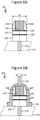
- Figures 6A-6B illustrate additional processing of the IC 100 of Figure 5 to provide an IC 101, in accordance with an example outside the scope of the claimed invention.
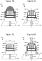
- Figures 7A-7D illustrate additional processing of the IC 100 of Figure 5 to provide an IC 102, in accordance with an embodiment of the present invention.
- IC 100 initially may include a first magnetic layer 105, a first insulator layer 120, a second magnetic layer 125, a second insulator layer 130, and a hardmask layer 135, each of which is discussed in turn below.
- These layers of IC 100 may be stacked as generally shown over an interconnect 115 of an underlying metallized circuit layer 110, in accordance with some embodiments.
- the lower interconnect 115 can be formed from any suitable electrically conductive material (or combination of materials), as typically done.
- Some example materials for lower interconnect 115 include: copper (Cu); cobalt (Co); molybdenum (Mo); rhodium (Rh); beryllium (Be); chromium (Cr); manganese (Mn); aluminum (Al); silver (Ag); gold (Au); titanium (Ti); indium (In); ruthenium (Ru); palladium (Pd); tungsten (W); nickel (Ni); and/or a combination of any one or more thereof. Also, the dimensions of lower interconnect 115 can be customized, as desired for a given target application or end-use.
- lower interconnect 115 may have a width/diameter (D 1 ) in the range of about 0.1-100 nm (e.g., about 0.1-1 nm, about 1-25 nm, about 25-50 nm, about 50-75 nm, about 75-100 nm, or any other sub-range in the range of about 0.1-100 nm).
- D 1 width/diameter
- Other suitable materials and configurations for lower interconnect 115 and underlying metallized circuit layer 110 will depend on a given application and will be apparent in light of this disclosure.
- first magnetic layer 105 may be prevented from undergoing changes in its magnetization, and thus may be considered, in a general sense, as being a fixed or pinned magnetic layer.
- first magnetic layer 105 hereinafter may be referred to as a fixed magnetic layer 105.
- Fixed magnetic layer 105 can have any of a wide range of configurations.
- fixed magnetic layer 105 may be formed from one or more layers including: iron (Fe); tantalum (Ta); ruthenium (Ru); cobalt (Co); a combination of one or more transition metals, such as cobalt-palladium (Co-Pd) or cobalt-platinum (Co-Pt); a combination of one or more transition metals and a metalloid, such as cobalt-iron-boron (CoFeB); and/or a combination of any one or more thereof.
- fixed magnetic layer 105 may be formed as a multi-layered stack of films.
- fixed magnetic layer 105 may be formed as a multi-layered stack including: a tantalum (Ta) or other conductive bottom electrode; a synthetic antiferromagnet (SAF) of cobalt-platinum (Co-Pt) alloy/ruthenium (Ru)/cobalt-platinum (Co-Pt) alloy; a tantalum (Ta) or other conductive metal spacer; and a cobalt-iron-boron (CoFeB) alloy or other suitable reference layer.
- fixed magnetic layer 105 alternatively may include cobalt-palladium (Co-Pd) within the SAF portion thereof.
- fixed magnetic layer 105 In some instances in which fixed magnetic layer 105 is configured as a multi-layered stack, some degree of intermixing may occur between constituent layers, for example, as a result of thermal annealing or other processing. In some cases, the constituent materials of a given portion of fixed magnetic layer 105 may be intentionally combined so as to provide an alloyed film; for instance, cobalt (Co), iron (Fe), and boron (B) may be sputtered together to provide a CoFeB alloy film. Other suitable materials and configurations for fixed magnetic layer 105 will depend on a given application and will be apparent in light of this disclosure.
- fixed magnetic layer 105 can be formed using any of a wide range of techniques.
- fixed magnetic layer 105 may be formed, in accordance with some embodiments, using: a physical vapor deposition (PVD) process, such as sputter deposition; a chemical vapor deposition (CVD) process; and/or a molecular beam epitaxy (MBE) process.
- PVD physical vapor deposition
- CVD chemical vapor deposition
- MBE molecular beam epitaxy
- the dimensions of fixed magnetic layer 105 can be customized as desired for a given target application or end-use.
- fixed magnetic layer 105 may have a thickness in the range of about 1-100 ⁇ (e.g., about 1-25 ⁇ , about 25-50 ⁇ , about 50-75 ⁇ , about 75-100 ⁇ , or any other sub-range in the range of about 1-100 ⁇ ). In some cases, fixed magnetic layer 105 may have a thickness of a monolayer of its one or more constituent materials. In some instances, fixed magnetic layer 105 may have a substantially uniform thickness over the topography provided, for example, by any underlying layers of IC 100 (e.g., metallized layer 110 and/or lower interconnect 115). In some instances, fixed magnetic layer 105 may be provided as a substantially conformal layer over such topography.
- fixed magnetic layer 105 may be provided with a non-uniform or otherwise varying thickness over such topography.
- a first portion of fixed magnetic layer 105 may have a thickness within a first range while a second portion thereof has a thickness within a second, different range.
- Other suitable dimensions and techniques for forming fixed magnetic layer 105 will depend on a given application and will be apparent in light of this disclosure.
- First insulator layer 120 can be formed from any suitable electrically insulating material (or combination of such materials), using any of a wide range of techniques.
- first insulator layer 120 may be formed from an electrically conductive oxide, such as magnesium oxide (MgO).
- first insulator layer 120 may be formed, for example, using: a physical vapor deposition (PVD) process, such as sputter deposition; a chemical vapor deposition (CVD) process; and/or a molecular beam epitaxy (MBE) process.
- PVD physical vapor deposition
- CVD chemical vapor deposition
- MBE molecular beam epitaxy
- Other suitable materials and techniques for forming first insulator layer 120 will depend on a given application and will be apparent in light of this disclosure.
- first insulator layer 120 can be customized as desired for a given target application or end-use.
- first insulator layer 120 may have a thickness in the range of about 1-100 ⁇ (e.g., about 1-25 ⁇ , about 25-50 ⁇ , about 50-75 ⁇ , about 75-100 ⁇ , or any other sub-range in the range of about 1-100 ⁇ ).
- first insulator layer 120 may have a thickness of a monolayer of its one or more constituent materials.
- first insulator layer 120 may be selected or otherwise tuned such that fixed magnetic layer 105 and second magnetic layer 125 are sufficiently insulated from one another while still allowing electrons to pass there between via quantum tunneling through first insulator layer 120.
- first insulator layer 120 may serve, at least in part, as a spin filter for the MTJ of IC 100.
- first insulator layer 120 may have a substantially uniform thickness over the topography provided, for example, by any underlying layers of IC 100 (e.g., fixed magnetic layer 105).
- first insulator layer 120 may be provided as a substantially conformal layer over such topography.
- first insulator layer 120 may be provided with a non-uniform or otherwise varying thickness over such topography. For example, in some cases a first portion of first insulator layer 120 may have a thickness within a first range while a second portion thereof has a thickness within a second, different range. In some cases, first insulator layer 120 may be formed from multiple layers of the same or different materials (e.g., an insulator material and a non-insulator material). Other suitable dimensions for first insulator layer 120 will depend on a given application and will be apparent in light of this disclosure.
- free magnetic layer 125 can be formed from any of the example magnetic materials discussed above, for instance, with respect to fixed magnetic layer 105, in accordance with some embodiments.
- free magnetic layer 125 may be formed as a single layer of CoFeB or a multi-layer stack of CoFeB/Ta/CoFeB.
- free magnetic layer 125 may be permitted to undergo changes in its magnetization, and thus may be considered, in a general sense, as being a free or dynamic magnetic layer.
- free magnetic layer 125 hereinafter may be referred to as a free magnetic layer 125.
- free magnetic layer 125 can be formed over IC 100 using any of the example formation techniques discussed above with reference to fixed magnetic layer 105, in accordance with some embodiments. Other suitable materials and techniques for forming free magnetic layer 125 will depend on a given application and will be apparent in light of this disclosure.
- free magnetic layer 125 can be customized as desired for a given target application or end-use.
- free magnetic layer 125 may have a thickness in the range of about 1-100 ⁇ (e.g., about 1-25 ⁇ , about 25-50 ⁇ , about 50-75 ⁇ , about 75-100 ⁇ , or any other sub-range in the range of about 1-100 ⁇ ).
- free magnetic layer 125 may have a thickness of a monolayer of its one or more constituent materials.
- free magnetic layer 125 may have a substantially uniform thickness over the topography provided, for example, by any underlying layers of IC 100 (e.g., first insulator layer 120).
- free magnetic layer 125 may be provided as a substantially conformal layer over such topography. In some other instances, free magnetic layer 125 may be provided with a non-uniform or otherwise varying thickness over such topography. For example, in some cases a first portion of free magnetic layer 125 may have a thickness within a first range while a second portion thereof has a thickness within a second, different range. Other suitable dimensions for free magnetic layer 125 will depend on a given application and will be apparent in light of this disclosure.
- Second insulator layer 130 can be formed from any of a wide range of materials.
- second insulator layer 130 may be formed from an electrically conductive oxide, such as magnesium oxide (MgO), tantalum oxide (Ta 2 O 5 ), aluminum oxide (Al 2 O 3 ), and/or a combination of any one or more thereof.
- second insulator layer 130 can be formed over IC 100 using any of the example formation techniques discussed above with reference to first insulator layer 120, in accordance with some embodiments.
- second insulator layer 130 can be formed over IC 100 using an atomic layer deposition (ALD) process.
- ALD atomic layer deposition
- Other suitable materials and techniques for forming second insulator layer 130 will depend on a given application and will be apparent in light of this disclosure.
- second insulator layer 130 can be customized as desired for a given target application or end-use.
- second insulator layer 130 may have a thickness in one or more of the example ranges discussed above, for instance, with respect to first insulator layer 120.
- second insulator layer 130 may have a thickness that is substantially equivalent to (e.g., exactly equal to or otherwise within a given tolerance of) the thickness of first insulator layer 120.
- second insulator layer 130 may have a thickness of a monolayer of its one or more constituent materials.
- second insulator layer 130 may have a substantially uniform thickness over the topography provided, for example, by any underlying layers of IC 100 (e.g., free magnetic layer 125).
- second insulator layer 130 may be provided as a substantially conformal layer over such topography. In some other instances, second insulator layer 130 may be provided with a non-uniform or otherwise varying thickness over such topography. For example, in some cases a first portion of second insulator layer 130 may have a thickness within a first range while a second portion thereof has a thickness within a second, different range. In some cases, second insulator layer 130 may be formed from multiple layers of the same or different materials (e.g., an insulator material and a non-insulator material). Other suitable dimensions for second insulator layer 130 will depend on a given application and will be apparent in light of this disclosure.
- Hardmask layer 135 can be formed from any suitable hardmask material (or combination of such materials), using any of a wide range of techniques.
- hardmask layer 135 may be formed from a metal, such as: tungsten (W); tantalum (Ta); titanium (Ti); ruthenium (Ru); and/or a combination of any one or more thereof.
- hardmask layer 135 may be formed from a nitride, such as: titanium nitride (TiN); tantalum nitride (TaN); and/or a combination of any one or more thereof.
- hardmask layer 135 may be formed using: a physical vapor deposition (PVD) process, such as sputter deposition; and/or an atomic layer deposition (ALD) process.
- PVD physical vapor deposition
- ALD atomic layer deposition
- Other suitable materials and techniques for forming hardmask layer 135 will depend on a given application and will be apparent in light of this disclosure.
- hardmask layer 135 can be customized as desired for a given target application or end-use.
- hardmask layer 135 may have a thickness in the range of about 1-200 nm (e.g., about 1-50 nm, about 50-100 nm, about 100-150 nm, about 150-200 nm, or any other sub-range in the range of about 1-200 nm).
- hardmask layer 135 may have a substantially uniform thickness over the topography provided, for example, by any underlying layers of IC 100 (e.g., second insulator layer 130).
- hardmask layer 135 may be provided as a substantially conformal layer over such topography.
- hardmask layer 135 may be provided with a non-uniform or otherwise varying thickness over such topography. For example, in some cases a first portion of hardmask layer 135 may have a thickness within a first range while a second portion thereof has a thickness within a second, different range. Other suitable dimensions for hardmask layer 135 will depend on a given application and will be apparent in light of this disclosure.
- FIG. 2 is a cross-sectional view of the IC 100 of Figure 1 after patterning of hardmask layer 135, in accordance with an embodiment of the present disclosure.
- Patterning of hardmask layer 135 can be performed using any suitable standard and/or custom patterning process, as will be apparent in light of this disclosure.
- hardmask layer 135 may be patterned, for example, using: a reactive-ion etching (RIE) process; and/or an ion milling process.
- RIE reactive-ion etching
- the etch chemistry utilized in patterning hardmask layer 135 can be customized, as desired for a given target application or end-use.
- a dry plasma-based etch process may be utilized in anisotropically etching hardmask layer 135.
- the resultant hardmask layer 135' may have a width/diameter ( D 2 ) in the range of about 1-100 nm (e.g., about 1-25 nm, about 25-50 nm, about 50-75 nm, about 75-100 nm, or any other sub-range in the range of about 1-100 nm).
- patterned hardmask layer 135' may provide a dot contact for underlying patterned free magnetic layer 125'.
- Other suitable techniques for patterning hardmask layer 135 will depend on a given application and will be apparent in light of this disclosure.
- First spacer layer 140 can be formed from any suitable dielectric material (or combination of such materials), using any of a wide range of techniques.
- first spacer layer 140 may be formed from: an oxide, such as silicon dioxide (SiO 2 ); a nitride, such as silicon nitride (Si 3 N 4 ), titanium nitride (TiN), and/or silicon carbon nitride (SiCN); an oxynitride, such as silicon oxynitride (SiO x N y ); and/or a combination of any one or more thereof.
- first spacer layer 140 may be formed using: a chemical vapor deposition (CVD) process; and/or an atomic layer deposition (ALD) process.
- CVD chemical vapor deposition
- ALD atomic layer deposition
- first spacer layer 140 can be customized as desired for a given target application or end-use.
- first spacer layer 140 may have a substantially uniform thickness over the topography provided, for example, by any underlying layers of IC 100 (e.g., patterned hardmask layer 135' and/or second insulator layer 130).
- first spacer layer 140 may be provided as a substantially conformal layer over such topography.
- first spacer layer 140 may be provided with a non-uniform or otherwise varying thickness over such topography.
- a first portion of first spacer layer 140 may have a thickness within a first range while a second portion thereof has a thickness within a second, different range.
- Other suitable dimensions for first spacer layer 140 will depend on a given application and will be apparent in light of this disclosure.
- first spacer layer 140 may be patterned, for example, using a reactive-ion etching (RIE) process.
- RIE reactive-ion etching
- the etch chemistry utilized in patterning first spacer layer 140 can be customized, as desired for a given target application or end-use.
- a dry plasma-based etch process may be utilized in anisotropically etching first spacer layer 140.
- first spacer layer 140' may have a generally cylindrical geometry that may be generally circular in cross-sectional profile, in some embodiments. In some other embodiments, first spacer layer 140' may have a generally cylindrical geometry that may be generally elliptical in cross-sectional profile. In some still other embodiments, first spacer layer 140' may have a generally tubular geometry that may be generally circular-annular or elliptical-annular in cross-sectional profile, in some embodiments.
- first spacer layer 140' may have a sidewall thickness ( D 3 ) in the range of about 1-20 nm (e.g., about 1-5 nm, about 5-10 nm, about 10-15 nm, about 15-20 nm, or any other sub-range in the range of about 1-20 nm).
- D 3 sidewall thickness
- Other suitable techniques for patterning first spacer layer 140 will depend on a given application and will be apparent in light of this disclosure.
- FIG. 5 is a cross-sectional view of the IC 100 of Figure 4 after patterning second insulator layer 130, free magnetic layer 125, and first insulator layer 120, in accordance with an embodiment of the present disclosure.
- Patterning of second insulator layer 130, free magnetic layer 125, and first insulator layer 120 can be performed, in accordance with some embodiments, using any suitable standard and/or custom patterning process, as will be apparent in light of this disclosure.
- second insulator layer 130, free magnetic layer 125, and first insulator layer 120 may be patterned, for example, using: a reactive-ion etching (RIE) process; and/or an ion milling process.
- RIE reactive-ion etching
- the etch chemistry utilized in patterning second insulator layer 130, free magnetic layer 125, and first insulator layer 120 can be customized, as desired for a given target application or end-use.
- a dry plasma-based etch process may be utilized in anisotropically etching second insulator layer 130, free magnetic layer 125, and first insulator layer 120.
- the resultant second insulator layer 130', free magnetic layer 125', and first insulator layer 120' may have a generally cylindrical geometry that may be generally circular in cross-sectional profile, in some embodiments.
- second insulator layer 130', free magnetic layer 125', and first insulator layer 120' may have a generally cylindrical geometry that may be generally elliptical in cross-sectional profile.
- patterning (e.g., etching) of free magnetic layer 125 may stop above an upper surface of the underlying first insulator layer 120. In some other instances, however, patterning (e.g., etching) of free magnetic layer 125 may stop below a lower surface of the underlying first insulator layer 120.
- second insulator layer 130', free magnetic layer 125', and first insulator layer 120' may have a width/diameter ( D 4 ) in the range of about 1-100 nm (e.g., about 1-25 nm, about 25-50 nm, about 50-75 nm, about 75-100 nm, or any other sub-range in the range of about 1-100 nm).
- the width/diameter ( D 4 ) of second insulator layer 130', free magnetic layer 125', and first insulator layer 120' may depend, at least in part, on the sidewall thickness ( D 3 ) of patterned first spacer layer 140', discussed above.
- patterned first spacer layer 140' may serve, at least in part, to ensure that patterned hardmask layer 135' is substantially center-aligned (e.g., exactly center-aligned or otherwise within a given tolerance) with respect to second insulator layer 130', free magnetic layer 125', and first insulator layer 120', in accordance with an embodiment.
- Other suitable techniques for patterning second insulator layer 130, free magnetic layer 125, and first insulator layer 120 will depend on a given application and will be apparent in light of this disclosure.
- Figures 6A-6B illustrate additional processing of the IC 100 of Figure 5 to provide an IC 101, in accordance with an example outside the scope of the claimed invention.
- the process may continue as in Figure 6A , which is a cross-sectional view of the IC 100 of Figure 5 after patterning fixed magnetic layer 105.
- patterning of fixed magnetic layer 105 may be performed using any of the example techniques discussed above, for instance, with respect to free magnetic layer 125.
- the resultant fixed magnetic layer 105' may have a generally cylindrical geometry that may be generally circular in cross-sectional profile.
- fixed magnetic layer 105' may have a generally cylindrical geometry that may be generally elliptical in cross-sectional profile.
- patterned fixed magnetic layer 105' may have a width/diameter ( D 4 ) in the range of about 1-100 nm (e.g., about 1-25 nm, about 25-50 nm, about 50-75 nm, about 75-100 nm, or any other sub-range in the range of about 1-100 nm).
- the width/diameter ( D 4 ) of fixed magnetic layer 105' may depend, at least in part, on the sidewall thickness ( D 3 ) of patterned first spacer layer 140', discussed above.
- patterned first spacer layer 140' may be utilized in patterning (e.g., etching) the fixed magnetic layer 105 of the MTJ device of IC 101. Also, in a general sense, patterned first spacer layer 140' may serve, at least in part, to ensure that patterned hardmask layer 135' is substantially center-aligned (e.g., exactly center-aligned or otherwise within a given tolerance) with respect to patterned fixed magnetic layer 105'.
- Encapsulation layer 150 can be formed from any suitable material (or combination of materials), using any of a wide range of techniques.
- encapsulation layer 150 may be formed from: an oxide, such as aluminum oxide (Al 2 O 3 ) and/or tantalum oxide (Ta 2 O 5 ); a nitride, such as silicon nitride (Si 3 N 4 ), titanium nitride (TiN), and/or silicon carbon nitride (SiCN); and/or a combination of any one or more thereof.
- Encapsulation layer 150 may be formed using: a chemical vapor deposition (CVD) process; and/or an atomic layer deposition (ALD) process. Other suitable materials and techniques for forming encapsulation layer 150 will depend on a given application and will be apparent in light of this disclosure.
- CVD chemical vapor deposition
- ALD atomic layer deposition
- encapsulation layer 150 of IC 101 can be customized as desired for a given target application or end-use.
- encapsulation layer 150 may have a substantially uniform thickness over the topography provided, for example, by any underlying layers of IC 101 (e.g., patterned hardmask layer 135', patterned first spacer layer 140', patterned second insulator layer 130', patterned free magnetic layer 125', patterned first insulator layer 120', patterned fixed magnetic layer 105', and/or metallized circuit layer 110).
- encapsulation layer 150 may have a substantially uniform thickness over the topography provided, for example, by any underlying layers of IC 101 (e.g., patterned hardmask layer 135', patterned first spacer layer 140', patterned second insulator layer 130', patterned free magnetic layer 125', patterned first insulator layer 120', patterned fixed magnetic layer 105', and/or metallized circuit layer 110).
- encapsulation layer 150 may be provided as a substantially conformal layer over such topography.
- encapsulation layer 150 may be provided with a nonuniform or otherwise varying thickness over such topography.
- a first portion of encapsulation layer 150 may have a thickness within a first range while a second portion thereof has a thickness within a second, different range.
- Other suitable dimensions for encapsulation layer 150 of IC 101 will depend on a given application and will be apparent in light of this disclosure.
- upper interconnect 155 can be formed from any of the example electrically conductive materials discussed above, for instance, with respect to lower interconnect 115. Also, as will be appreciated, upper interconnect 155 can be formed over IC 101 using any of the example formation techniques discussed above with reference to lower interconnect 115. As will be appreciated further, the dimensions of upper interconnect 155 can be customized, as desired for a given target application or end - use.
- upper interconnect 155 may have a width/diameter (D 5 ) in the range of about 0.1-100 nm (e.g., about 0.1-1 nm, about 1-25 nm, about 25-50 nm, about 50-75 nm, about 75-100 nm, or any other sub-range in the range of about 0.1-100 nm).
- upper interconnect 155 may have a width/diameter (D ⁇ j) that is substantially equivalent to (e.g., exactly equal to or otherwise within a given tolerance of) the width/diameter (D) of lower interconnect 115.
- the width/diameter (Dj) of upper interconnect 155 may be less than or about equal to the width/diameter (i3/4) of patterned hardmask layer 135'. In some other cases, the width/diameter (D5) of upper interconnect 155 may be greater than the width/diameter (i3/4) of patterned hardmask layer 135'.
- Other suitable materials, configurations, and techniques for forming upper interconnect 155 will depend on a given application and will be apparent in light of this disclosure.
- Figures 7A-7D illustrate additional processing of the IC 100 of Figure 5 to provide an IC 102.
- Figure 7A is a cross-sectional view of the IC 100 of Figure 5 after formation of a second spacer layer 145, in accordance with an embodiment of the present invention.
- second spacer layer 145 can be formed from any of the example dielectric materials discussed above, for instance, with respect to first spacer layer 140, in accordance with some embodiments.
- second spacer layer 145 can be formed over IC 102 using any of the example formation techniques discussed above with reference to first spacer layer 140, in accordance with some embodiments.
- Other suitable materials and techniques for forming second spacer layer 145 will depend on a given application and will be apparent in light of this disclosure.
- second spacer layer 145 can be customized as desired for a given target application or end-use.
- second spacer layer 145 may have a substantially uniform thickness over the topography provided, for example, by any underlying layers of IC 102 (e.g., patterned hardmask layer 135', patterned first spacer layer 140', patterned second insulator layer 130', patterned free magnetic layer 125', patterned first insulator layer 120', and/or fixed magnetic layer 105).
- second spacer layer 145 may be provided as a substantially conformal layer over such topography.
- second spacer layer 145 may be provided with a non-uniform or otherwise varying thickness over such topography.
- first portion of second spacer layer 145 may have a thickness within a first range while a second portion thereof has a thickness within a second, different range.
- Other suitable dimensions for second spacer layer 145 will depend on a given application and will be apparent in light of this disclosure.
- Figure 7B is a cross-sectional view of the IC 102 of Figure 7 A after patterning second spacer layer 145, in accordance with an embodiment of the present invention.
- second spacer layer 145 can be patterned using any of the example patterning techniques and etch chemistries discussed above with reference to first spacer layer 140, in accordance with some embodiments.
- the resultant second spacer layer 145' may have a generally cylindrical geometry that may be generally circular in cross-sectional profile, in some embodiments. In some other embodiments, second spacer layer 145' may have a generally cylindrical geometry that may be generally elliptical in cross-sectional profile.
- second spacer layer 145' may have a generally tubular geometry that may be generally circular-annular or elliptical-annular in cross-sectional profile, in some embodiments.
- second spacer layer 145' may have a sidewall thickness (Dg) in the range of about 1-20 nm (e.g., about 1-5 nm, about 5-10 nm, about 10-15 nm, about 15-20 nm, or any other sub-range in the range of about 1-20 nm).
- Dg sidewall thickness
- Other suitable techniques for patterning second spacer layer 145 will depend on a given application and will be apparent in light of this disclosure.
- a lower portion 147' (e.g., the foot or base portion) of patterned second spacer layer 145' may land at a location along the sidewalls of the MTJ device of IC 102 that is below patterned first insulator layer 120' and above fixed magnetic layer 105, in accordance with some embodiments. It should be noted, however, that the present disclosure is not so limited. For instance, in accordance with some other embodiments, a lower portion 147' of patterned second spacer layer 145' may land at a location along the sidewalls of the MTJ device of IC 102 that is below patterned free magnetic layer 125' and above patterned first insulator layer 120'.
- a lower portion 147' of patterned second spacer layer 145' may land at any location along the sidewalls of the MTJ device of IC 102 that is below patterned free magnetic layer 125' and above patterned first insulator layer 120'.
- a lower portion 147' of patterned second spacer layer 145' may land at any location along the sidewalls of the MTJ device of IC 102 that does not expose patterned free magnetic layer 125' to redepositing of etch byproducts during patterning of fixed magnetic layer 105, as discussed below.
- Figure 7C is a cross-sectional view of the IC 102 of Figure 7B after patterning fixed magnetic layer 105, in accordance with an embodiment of the present invention.
- underlying fixed magnetic layer 105 may undergo patterning.
- patterned second spacer layer 145' may serve, at least in part, to protect the sidewalls of patterned free magnetic layer 125' (and/or other layers of the MTJ of IC 102) from redepositing of residual etch byproducts during patterning of fixed magnetic layer 105.
- patterned second spacer layer 145' may be configured to prevent or otherwise reduce any susceptibility to electrical shorting between the patterned free magnetic layer 125' and the patterned fixed magnetic layer 105' of the MTJ of IC 102.
- patterned fixed magnetic layer 105' may have a width/diameter ( D 7 ) in the range of about 1-100 nm (e.g., about 1-25 nm, about 25-50 nm, about 50-75 nm, about 75-100 nm, or any other sub-range in the range of about 1-100 nm).
- the width/diameter ( D 7 ) of fixed magnetic layer 105' may depend, at least in part, on the sidewall thickness (D 6 ) of patterned second spacer layer 145', discussed above.
- patterned second spacer layer 145' may be utilized in patterning (e.g., etching) the fixed magnetic layer 105 of the MTJ device of IC 102.
- the dual spacer combination of patterned second spacer layer 145' and patterned first spacer layer 140' may be utilized in patterning the fixed magnetic layer 105 of the MTJ device of IC 102.
- encapsulation layer 150 of IC 102 can be customized as desired for a given target application or end-use.
- encapsulation layer 150 may have a substantially uniform thickness over the topography provided, for example, by any underlying layers of IC 102 (e.g., patterned hardmask layer 135', patterned first spacer layer 140', patterned second spacer layer 145', patterned fixed magnetic layer 105', and/or metallized circuit layer 110).
- encapsulation layer 150 may be provided as a substantially conformal layer over such topography. In some other instances, encapsulation layer 150 may be provided with a non-uniform or otherwise varying thickness over such topography. For example, in some cases a first portion of encapsulation layer 150 may have a thickness within a first range while a second portion thereof has a thickness within a second, different range. Other suitable dimensions for encapsulation layer 150 of IC 102 will depend on a given application and will be apparent in light of this disclosure.
- FIG 8 illustrates a computing system 1000 implemented with integrated circuit structures or devices formed using the disclosed techniques in accordance with an example embodiment.
- the computing system 1000 houses a motherboard 1002.
- the motherboard 1002 may include a number of components, including, but not limited to, a processor 1004 and at least one communication chip 1006, each of which can be physically and electrically coupled to the motherboard 1002, or otherwise integrated therein.
- the motherboard 1002 may be, for example, any printed circuit board, whether a main board, a daughterboard mounted on a main board, or the only board of system 1000, etc.
- computing system 1000 may include one or more other components that may or may not be physically and electrically coupled to the motherboard 1002.
- volatile memory e.g., DRAM
- non-volatile memory e.g., ROM
- graphics processor e.g., a digital signal processor, a crypto processor, a chipset, an antenna, a display, a touchscreen display, a touchscreen controller, a battery, an audio codec, a video codec, a power amplifier, a global positioning system (GPS) device, a compass, an accelerometer, a gyroscope, a speaker, a camera, and a mass storage device (such as hard disk drive, compact disk (CD), digital versatile disk (DVD), and so forth).
- any of the components included in computing system 1000 may include one or more integrated circuit structures or devices formed using the disclosed techniques in accordance with an example embodiment.
- multiple functions can be integrated into one or more chips (e.g., for instance, note that the communication chip 1006 can be part of or otherwise integrated into the processor 1004).
- the communication chip 1006 enables wireless communications for the transfer of data to and from the computing system 1000.
- wireless and its derivatives may be used to describe circuits, devices, systems, methods, techniques, communications channels, etc., that may communicate data through the use of modulated electromagnetic radiation through a non-solid medium. The term does not imply that the associated devices do not contain any wires, although in some embodiments they might not.
- the communication chip 1006 may implement any of a number of wireless standards or protocols, including, but not limited to, Wi-Fi (IEEE 802.11 family), WiMAX (IEEE 802.16 family), IEEE 802.20, long term evolution (LTE), Ev-DO, HSPA+, HSDPA+, HSUPA+, EDGE, GSM, GPRS, CDMA, TDMA, DECT, Bluetooth, derivatives thereof, as well as any other wireless protocols that are designated as 3G, 4G, 5G, and beyond.
- the computing system 1000 may include a plurality of communication chips 1006.
- a first communication chip 1006 may be dedicated to shorter range wireless communications such as Wi-Fi and Bluetooth and a second communication chip 1006 may be dedicated to longer range wireless communications such as GPS, EDGE, GPRS, CDMA, WiMAX, LTE, Ev-DO, and others.
- the processor 1004 of the computing system 1000 includes an integrated circuit die packaged within the processor 1004.
- the integrated circuit die of the processor includes onboard circuitry that is implemented with one or more integrated circuit structures or devices formed using the disclosed techniques, as variously described herein.
- the term "processor" may refer to any device or portion of a device that processes, for instance, electronic data from registers and/or memory to transform that electronic data into other electronic data that may be stored in registers and/or memory.
- the communication chip 1006 also may include an integrated circuit die packaged within the communication chip 1006.
- the integrated circuit die of the communication chip includes one or more integrated circuit structures or devices formed using the disclosed techniques as described herein.
- multi-standard wireless capability may be integrated directly into the processor 1004 (e.g., where functionality of any chips 1006 is integrated into processor 1004, rather than having separate communication chips).
- processor 1004 may be a chip set having such wireless capability.
- any number of processor 1004 and/or communication chips 1006 can be used.
- any one chip or chip set can have multiple functions integrated therein.
- the computing device 1000 may be a laptop, a netbook, a notebook, a smartphone, a tablet, a personal digital assistant (PDA), an ultra-mobile PC, a mobile phone, a desktop computer, a server, a printer, a scanner, a monitor, a set-top box, an entertainment control unit, a digital camera, a portable music player, a digital video recorder, or any other electronic device that processes data or employs one or more integrated circuit structures or devices formed using the disclosed techniques, as variously described herein.
- PDA personal digital assistant
Landscapes
- Engineering & Computer Science (AREA)
- Computer Hardware Design (AREA)
- Manufacturing & Machinery (AREA)
- Mram Or Spin Memory Techniques (AREA)
- Hall/Mr Elements (AREA)
Claims (13)
- Circuit intégré (102), comprenant :une jonction tunnel magnétique (MTJ) comprenant une couche magnétique fixe (105) ;une première couche isolante (120) formée sur la couche magnétique fixe (105) ; etune couche magnétique libre (125) formée sur la première couche isolante (120) ;une deuxième couche isolante (130) formée sur la couche magnétique libre (125) ;une couche de masque rigide électroconductrice (135) formée sur la deuxième couche isolante (130), dans lequel la couche de masque rigide (135) présente une largeur/un diamètre qui est inférieur(e) à une largeur/un diamètre de la couche magnétique libre (125) ;un premier élément d'espacement diélectrique (140) formé sur la deuxième couche isolante (130) et couvrant les parois latérales de la couche de masque rigide (135) ;caractérisé par un deuxième élément d'espacement diélectrique (145) formé sur la couche magnétique fixe (105) et couvrant les parois latérales de la couche magnétique libre (125).
- Circuit intégré (102) selon la revendication 1, dans lequel la couche magnétique fixe (105) est couplée de manière électronique à une interconnexion (115) sous-jacente, et dans lequel la couche magnétique libre (125) est couplée de manière électronique à une interconnexion superposée (155).
- Circuit intégré (102) selon l'une quelconque des revendications 1 et 2, dans lequel chacune de la couche magnétique libre (125) et de la couche de masque rigide (135) présente une largeur/un diamètre dans la plage d'environ 1 à 100 nm.
- Circuit intégré (102) selon l'une quelconque des revendications 1 à 3, dans lequel la couche de masque rigide (135) est centrée par rapport à la couche magnétique libre (125).
- Circuit intégré (102) selon l'une quelconque des revendications 1 à 4, dans lequel le premier élément d'espacement diélectrique (140) présente une géométrie cylindrique à profil circulaire ou elliptique en section transversale.
- Circuit intégré (102) selon l'une quelconque des revendications 1 à 5, dans lequel le deuxième élément d'espacement diélectrique (145) présente une géométrie cylindrique à profil circulaire ou elliptique en section transversale.
- Circuit intégré (102) selon l'une quelconque des revendications 1 à 6, comprenant en outre une couche d'encapsulation (150) formée sur une topographie fournie par celle-ci.
- Procédé de formation d'un circuit intégré (102), le procédé comprenant les étapes consistant à :former une jonction tunnel magnétique (MTJ) comprenant une couche magnétique fixe (105), une première couche isolante (120) sur la couche magnétique fixe (105) et une couche magnétique libre (125) sur la première couche isolante (120) ;former une deuxième couche isolante (130) sur la couche magnétique libre (125) ;former une couche de masque rigide électroconductrice (135) sur la deuxième couche isolante (130), dans lequel la couche de masque rigide (135) présente une largeur/un diamètre qui est inférieur(e) à une largeur/un diamètre de la couche magnétique libre (125) ;former un premier élément d'espacement diélectrique (140) sur la deuxième couche isolante (130) et couvrir les parois latérales de la couche de masque rigide (135) ;caractérisé par la formation d'un deuxième élément d'espacement diélectrique (145) sur la couche magnétique fixe (105) et la couverture des parois latérales de la couche magnétique libre (125).
- Procédé selon la revendication 8, comprenant en outre :
la configuration de la couche magnétique fixe (105) pour réduire sa largeur/son diamètre à une dimension approximativement égale à une largeur/un diamètre de la couche magnétique libre (125). - Procédé selon l'une quelconque des revendications 8 et 9, dans lequel la formation de la couche de masque rigide (135) comprend :le dépôt de la couche de masque rigide (135) sur une topographie fournie par la deuxième couche isolante (130) ; etla configuration de la couche de masque rigide (135) pour réduire sa largeur/son diamètre à une dimension approximativement égale à une largeur/un diamètre de la deuxième couche isolante (130).
- Procédé selon l'une quelconque des revendications 8 à 10, dans lequel la formation du premier élément d'espacement diélectrique (140) comprend :le dépôt du premier élément d'espacement diélectrique (140) sur une topographie fournie par la couche de masque rigide (135) et la deuxième couche isolante (130) ; etla configuration du premier élément d'espacement diélectrique (140) pour réduire ses dimensions pour couvrir les parois latérales de la couche de masque rigide (135).
- Procédé selon l'une quelconque des revendications 8 à 12, dans lequel la formation du deuxième élément d'espacement diélectrique (145) comprend :le dépôt du deuxième élément d'espacement diélectrique (145) sur une topographie fournie par la couche de masque rigide (135), le premier élément d'espacement diélectrique (140), la deuxième couche isolante (130) et la couche magnétique libre (125) ; etla configuration du deuxième élément d'espacement diélectrique (145) de sorte qu'une partie inférieure du deuxième élément d'espacement diélectrique (145) se trouve soit :au-dessous des parois latérales de la couche magnétique libre (125) et au-dessus des parois latérales de la première couche isolante (120) ; soitau-dessous des parois latérales de la première couche isolante (120) et au-dessus des parois latérales de la couche magnétique fixe (105).
- Procédé selon la revendication 12, comprenant en outre :
la configuration de la couche magnétique fixe (105) pour réduire sa largeur/son diamètre à une dimension supérieure à une largeur/un diamètre de la couche magnétique libre (125).
Applications Claiming Priority (1)
| Application Number | Priority Date | Filing Date | Title |
|---|---|---|---|
| PCT/US2014/032138 WO2015147855A1 (fr) | 2014-03-28 | 2014-03-28 | Techniques pour former une mémoire à couple de transfert de spin ayant une couche magnétique libre à points de contact |
Publications (3)
| Publication Number | Publication Date |
|---|---|
| EP3123476A1 EP3123476A1 (fr) | 2017-02-01 |
| EP3123476A4 EP3123476A4 (fr) | 2017-11-15 |
| EP3123476B1 true EP3123476B1 (fr) | 2019-10-16 |
Family
ID=54196171
Family Applications (1)
| Application Number | Title | Priority Date | Filing Date |
|---|---|---|---|
| EP14887032.2A Active EP3123476B1 (fr) | 2014-03-28 | 2014-03-28 | Techniques pour former une mémoire à couple de transfert de spin ayant une couche magnétique libre à contact ponctuel |
Country Status (6)
| Country | Link |
|---|---|
| US (2) | US9882121B2 (fr) |
| EP (1) | EP3123476B1 (fr) |
| KR (1) | KR102312731B1 (fr) |
| CN (1) | CN106062880A (fr) |
| TW (1) | TWI564888B (fr) |
| WO (1) | WO2015147855A1 (fr) |
Families Citing this family (23)
| Publication number | Priority date | Publication date | Assignee | Title |
|---|---|---|---|---|
| US9882121B2 (en) | 2014-03-28 | 2018-01-30 | Intel Corporation | Techniques for forming spin-transfer torque memory having a dot-contacted free magnetic layer |
| US9954165B2 (en) * | 2015-01-09 | 2018-04-24 | Hewlett Packard Enterprise Development Lp | Sidewall spacers |
| US10707411B1 (en) | 2015-06-19 | 2020-07-07 | Marvell International Ltd. | MRAM structure for efficient manufacturability |
| US20170069832A1 (en) * | 2015-09-03 | 2017-03-09 | Yong-Jae Kim | Magnetoresistive memory devices and methods of manufacturing the same |
| EP3350850A4 (fr) * | 2015-09-18 | 2019-05-08 | INTEL Corporation | Mémoire à couple de transfert de spin (sttm), ses procédés de formation à l'aide d'un isolant non conforme, et dispositifs l'incluant |
| CN108292705B (zh) | 2015-11-27 | 2022-01-18 | Tdk株式会社 | 自旋流磁化反转元件、磁阻效应元件及磁存储器 |
| US10304603B2 (en) * | 2016-06-29 | 2019-05-28 | International Business Machines Corporation | Stress control in magnetic inductor stacks |
| US10811177B2 (en) | 2016-06-30 | 2020-10-20 | International Business Machines Corporation | Stress control in magnetic inductor stacks |
| WO2018004680A1 (fr) | 2016-07-01 | 2018-01-04 | Intel Corporation | Dispositifs finfet et à trois grilles à bord de grille auto-aligné |
| US10879456B2 (en) * | 2018-06-27 | 2020-12-29 | Taiwan Semiconductor Manufacturing Co., Ltd. | Sidewall spacer stack for magnetic tunnel junctions |
| US10714680B2 (en) | 2018-08-27 | 2020-07-14 | Taiwan Semiconductor Manufacturing Company, Ltd. | Large height tree-like sub 30nm vias to reduce conductive material re-deposition for sub 60nm MRAM devices |
| US10516102B1 (en) * | 2018-10-16 | 2019-12-24 | Taiwan Semiconductor Manufacturing Company, Ltd. | Multiple spacer assisted physical etching of sub 60nm MRAM devices |
| US10726892B2 (en) | 2018-12-06 | 2020-07-28 | Sandisk Technologies Llc | Metallic magnetic memory devices for cryogenic operation and methods of operating the same |
| CN111952440B (zh) * | 2019-05-16 | 2023-04-07 | 中电海康集团有限公司 | Mram器件的制造方法 |
| US10923652B2 (en) * | 2019-06-21 | 2021-02-16 | Applied Materials, Inc. | Top buffer layer for magnetic tunnel junction application |
| JP2021044359A (ja) * | 2019-09-10 | 2021-03-18 | キオクシア株式会社 | 磁気記憶装置 |
| US11145808B2 (en) * | 2019-11-12 | 2021-10-12 | Applied Materials, Inc. | Methods for etching a structure for MRAM applications |
| US11437431B2 (en) * | 2020-01-15 | 2022-09-06 | Taiwan Semiconductor Manufacturing Company Limited | Memory device with flat-top bottom electrodes and methods for forming the same |
| US12414477B2 (en) * | 2021-04-09 | 2025-09-09 | Taiwan Semiconductor Manufacturing Company, Ltd. | Magnetic random access memory and manufacturing method thereof |
| CN115249764A (zh) * | 2021-04-28 | 2022-10-28 | 浙江驰拓科技有限公司 | 一种硬掩模的制备方法及磁随机存储器的制备方法 |
| US12317752B2 (en) * | 2021-05-12 | 2025-05-27 | International Business Machines Corporation | MRAM structure with multilayer encapsulation |
| US12069963B2 (en) * | 2021-08-30 | 2024-08-20 | Taiwan Semiconductor Manufacturing Company, Ltd. | Magnetic random access memory device and formation method thereof |
| KR102889766B1 (ko) | 2025-06-23 | 2025-11-20 | 곽영민 | 난삭재용 cnc 가공 시스템 |
Family Cites Families (22)
| Publication number | Priority date | Publication date | Assignee | Title |
|---|---|---|---|---|
| US6897532B1 (en) * | 2002-04-15 | 2005-05-24 | Cypress Semiconductor Corp. | Magnetic tunneling junction configuration and a method for making the same |
| KR100535046B1 (ko) * | 2002-12-30 | 2005-12-07 | 주식회사 하이닉스반도체 | 마그네틱 램의 형성방법 |
| US7112454B2 (en) * | 2003-10-14 | 2006-09-26 | Micron Technology, Inc. | System and method for reducing shorting in memory cells |
| US7381343B2 (en) | 2005-07-08 | 2008-06-03 | International Business Machines Corporation | Hard mask structure for patterning of materials |
| US7531367B2 (en) * | 2006-01-18 | 2009-05-12 | International Business Machines Corporation | Utilizing sidewall spacer features to form magnetic tunnel junctions in an integrated circuit |
| US8138561B2 (en) | 2008-09-18 | 2012-03-20 | Magic Technologies, Inc. | Structure and method to fabricate high performance MTJ devices for spin-transfer torque (STT)-RAM |
| US7939188B2 (en) * | 2008-10-27 | 2011-05-10 | Seagate Technology Llc | Magnetic stack design |
| CN102239562B (zh) * | 2008-12-08 | 2014-07-30 | Nxp股份有限公司 | 制造隧穿晶体管的方法和包括隧穿晶体管的ic |
| US7863060B2 (en) | 2009-03-23 | 2011-01-04 | Magic Technologies, Inc. | Method of double patterning and etching magnetic tunnel junction structures for spin-transfer torque MRAM devices |
| US7989224B2 (en) * | 2009-04-30 | 2011-08-02 | International Business Machines Corporation | Sidewall coating for non-uniform spin momentum-transfer magnetic tunnel junction current flow |
| US8513749B2 (en) * | 2010-01-14 | 2013-08-20 | Qualcomm Incorporated | Composite hardmask architecture and method of creating non-uniform current path for spin torque driven magnetic tunnel junction |
| US8981502B2 (en) * | 2010-03-29 | 2015-03-17 | Qualcomm Incorporated | Fabricating a magnetic tunnel junction storage element |
| US8133809B2 (en) | 2010-08-11 | 2012-03-13 | Magic Technologies, Inc. | Method to fabricate thin metal via interconnects on copper wires in MRAM devices |
| JP2013016587A (ja) * | 2011-07-01 | 2013-01-24 | Toshiba Corp | 磁気抵抗効果素子及びその製造方法 |
| US9245608B2 (en) | 2011-09-22 | 2016-01-26 | Qualcomm Incorporated | Thermally tolerant perpendicular magnetic anisotropy coupled elements for spin-transfer torque switching device |
| US8866242B2 (en) | 2011-11-10 | 2014-10-21 | Qualcomm Incorporated | MTJ structure and integration scheme |
| CN104137185B (zh) * | 2011-12-20 | 2018-01-12 | 英特尔公司 | 用于减小磁存储器元件接触部的尺寸和中心定位的方法 |
| US9172033B2 (en) * | 2013-07-03 | 2015-10-27 | Taiwan Semiconductor Manufacturing Company, Ltd. | MRAM device and fabrication method thereof |
| US9406875B2 (en) * | 2013-12-17 | 2016-08-02 | Qualcomm Incorporated | MRAM integration techniques for technology scaling |
| WO2015147813A1 (fr) * | 2014-03-26 | 2015-10-01 | Intel Corporation | Techniques de formation d'éléments de mémoire à couple de transfert de spin (sttm) comportant des contacts annulaires |
| US9882121B2 (en) | 2014-03-28 | 2018-01-30 | Intel Corporation | Techniques for forming spin-transfer torque memory having a dot-contacted free magnetic layer |
| US9972775B2 (en) * | 2015-03-12 | 2018-05-15 | Globalfoundries Singapore Pte. Ltd. | Integrated magnetic random access memory with logic device having low-k interconnects |
-
2014
- 2014-03-28 US US15/117,605 patent/US9882121B2/en not_active Expired - Fee Related
- 2014-03-28 EP EP14887032.2A patent/EP3123476B1/fr active Active
- 2014-03-28 KR KR1020167023143A patent/KR102312731B1/ko active Active
- 2014-03-28 CN CN201480076425.9A patent/CN106062880A/zh active Pending
- 2014-03-28 WO PCT/US2014/032138 patent/WO2015147855A1/fr not_active Ceased
-
2015
- 2015-02-09 TW TW104104230A patent/TWI564888B/zh active
-
2018
- 2018-01-29 US US15/882,546 patent/US10707409B2/en active Active
Non-Patent Citations (1)
| Title |
|---|
| None * |
Also Published As
| Publication number | Publication date |
|---|---|
| KR20160138387A (ko) | 2016-12-05 |
| US20180166625A1 (en) | 2018-06-14 |
| US9882121B2 (en) | 2018-01-30 |
| TWI564888B (zh) | 2017-01-01 |
| US10707409B2 (en) | 2020-07-07 |
| EP3123476A1 (fr) | 2017-02-01 |
| KR102312731B1 (ko) | 2021-10-15 |
| CN106062880A (zh) | 2016-10-26 |
| US20160359101A1 (en) | 2016-12-08 |
| TW201603016A (zh) | 2016-01-16 |
| WO2015147855A1 (fr) | 2015-10-01 |
| EP3123476A4 (fr) | 2017-11-15 |
Similar Documents
| Publication | Publication Date | Title |
|---|---|---|
| US10707409B2 (en) | Techniques for forming spin-transfer torque memory having a dot-contacted free magnetic layer | |
| KR102249872B1 (ko) | 환상 콘택트들을 갖는 스핀 전달 토크 메모리(sttm) 소자들을 형성하는 기술들 | |
| US10580973B2 (en) | Spin-transfer torque memory (STTM) devices having magnetic contacts | |
| US11430942B2 (en) | Multilayer free magnetic layer structure for spin-based magnetic memory | |
| CN103579496B (zh) | 磁性器件及其制造方法 | |
| CN106688117B (zh) | 用于垂直磁性隧道结器件的具有短接路径的氧化镁覆顶 | |
| JP2013517630A (ja) | 複合ハードマスク構造およびスピントルク駆動磁気トンネル接合のための不均一な電流経路を形成する方法 | |
| KR20190142201A (ko) | 개선된 보유 및 열 안정성을 갖는 수직 스핀 전달 토크 디바이스 | |
| US11171176B2 (en) | Asymmetric selector element for low voltage bipolar memory devices | |
| WO2019005082A1 (fr) | Dispositifs de jonction à effet tunnel magnétique avec dégazeur de paroi latérale | |
| WO2019005160A1 (fr) | Dispositifs de mémoire à couple de transfert de spin perpendiculaire (psttm) à électrode inférieure au nitrure de tantalate non stœchiométrique et leurs procédés de formation | |
| WO2019005128A1 (fr) | Dispositif de jonction à effet tunnel magnétique avec nano-contact à un aimant libre | |
| WO2019005157A1 (fr) | Dispositifs de mémoire de couple de transfert de spin perpendiculaire (psttm) à stabilité améliorée et à taux de magnétorésistance élevée à effet tunnel, et leurs procédés de formation | |
| WO2018101956A1 (fr) | Nano-contacts d'électrode auto-alignés pour cellules binaires de mémoire vive (ram) non volatile | |
| WO2018182669A1 (fr) | Dispositif de mémoire à registre à décalage de couplage d'orbite de spin |
Legal Events
| Date | Code | Title | Description |
|---|---|---|---|
| PUAI | Public reference made under article 153(3) epc to a published international application that has entered the european phase |
Free format text: ORIGINAL CODE: 0009012 |
|
| STAA | Information on the status of an ep patent application or granted ep patent |
Free format text: STATUS: REQUEST FOR EXAMINATION WAS MADE |
|
| 17P | Request for examination filed |
Effective date: 20160825 |
|
| AK | Designated contracting states |
Kind code of ref document: A1 Designated state(s): AL AT BE BG CH CY CZ DE DK EE ES FI FR GB GR HR HU IE IS IT LI LT LU LV MC MK MT NL NO PL PT RO RS SE SI SK SM TR |
|
| AX | Request for extension of the european patent |
Extension state: BA ME |
|
| RIN1 | Information on inventor provided before grant (corrected) |
Inventor name: CHAU, ROBERT, S. Inventor name: SURI, SATYARTH Inventor name: KUO, CHARLES, C. Inventor name: DOYLE, BRIAN, S. Inventor name: OGUZ, KAAN Inventor name: KENCKE, DAVID, L. Inventor name: DOCZY, MARK, L. |
|
| RIN1 | Information on inventor provided before grant (corrected) |
Inventor name: SURI, SATYARTH Inventor name: KENCKE, DAVID, L. Inventor name: DOCZY, MARK, L. Inventor name: CHAU, ROBERT, S. Inventor name: OGUZ, KAAN Inventor name: KUO, CHARLES, C. Inventor name: DOYLE, BRIAN, S. |
|
| DAX | Request for extension of the european patent (deleted) | ||
| REG | Reference to a national code |
Ref country code: DE Ref legal event code: R079 Ref document number: 602014055423 Country of ref document: DE Free format text: PREVIOUS MAIN CLASS: G11C0011160000 Ipc: H01L0043080000 |
|
| A4 | Supplementary search report drawn up and despatched |
Effective date: 20171018 |
|
| RIC1 | Information provided on ipc code assigned before grant |
Ipc: G11C 11/16 20060101ALI20171012BHEP Ipc: H01L 43/08 20060101AFI20171012BHEP Ipc: H01L 43/12 20060101ALI20171012BHEP |
|
| GRAP | Despatch of communication of intention to grant a patent |
Free format text: ORIGINAL CODE: EPIDOSNIGR1 |
|
| STAA | Information on the status of an ep patent application or granted ep patent |
Free format text: STATUS: GRANT OF PATENT IS INTENDED |
|
| INTG | Intention to grant announced |
Effective date: 20190516 |
|
| GRAS | Grant fee paid |
Free format text: ORIGINAL CODE: EPIDOSNIGR3 |
|
| GRAA | (expected) grant |
Free format text: ORIGINAL CODE: 0009210 |
|
| STAA | Information on the status of an ep patent application or granted ep patent |
Free format text: STATUS: THE PATENT HAS BEEN GRANTED |
|
| AK | Designated contracting states |
Kind code of ref document: B1 Designated state(s): AL AT BE BG CH CY CZ DE DK EE ES FI FR GB GR HR HU IE IS IT LI LT LU LV MC MK MT NL NO PL PT RO RS SE SI SK SM TR |
|
| REG | Reference to a national code |
Ref country code: GB Ref legal event code: FG4D |
|
| REG | Reference to a national code |
Ref country code: CH Ref legal event code: EP |
|
| REG | Reference to a national code |
Ref country code: DE Ref legal event code: R096 Ref document number: 602014055423 Country of ref document: DE |
|
| REG | Reference to a national code |
Ref country code: IE Ref legal event code: FG4D |
|
| REG | Reference to a national code |
Ref country code: AT Ref legal event code: REF Ref document number: 1192151 Country of ref document: AT Kind code of ref document: T Effective date: 20191115 |
|
| REG | Reference to a national code |
Ref country code: NL Ref legal event code: FP |
|
| REG | Reference to a national code |
Ref country code: LT Ref legal event code: MG4D |
|
| REG | Reference to a national code |
Ref country code: AT Ref legal event code: MK05 Ref document number: 1192151 Country of ref document: AT Kind code of ref document: T Effective date: 20191016 |
|
| PG25 | Lapsed in a contracting state [announced via postgrant information from national office to epo] |
Ref country code: AT Free format text: LAPSE BECAUSE OF FAILURE TO SUBMIT A TRANSLATION OF THE DESCRIPTION OR TO PAY THE FEE WITHIN THE PRESCRIBED TIME-LIMIT Effective date: 20191016 Ref country code: LT Free format text: LAPSE BECAUSE OF FAILURE TO SUBMIT A TRANSLATION OF THE DESCRIPTION OR TO PAY THE FEE WITHIN THE PRESCRIBED TIME-LIMIT Effective date: 20191016 Ref country code: PL Free format text: LAPSE BECAUSE OF FAILURE TO SUBMIT A TRANSLATION OF THE DESCRIPTION OR TO PAY THE FEE WITHIN THE PRESCRIBED TIME-LIMIT Effective date: 20191016 Ref country code: NO Free format text: LAPSE BECAUSE OF FAILURE TO SUBMIT A TRANSLATION OF THE DESCRIPTION OR TO PAY THE FEE WITHIN THE PRESCRIBED TIME-LIMIT Effective date: 20200116 Ref country code: GR Free format text: LAPSE BECAUSE OF FAILURE TO SUBMIT A TRANSLATION OF THE DESCRIPTION OR TO PAY THE FEE WITHIN THE PRESCRIBED TIME-LIMIT Effective date: 20200117 Ref country code: FI Free format text: LAPSE BECAUSE OF FAILURE TO SUBMIT A TRANSLATION OF THE DESCRIPTION OR TO PAY THE FEE WITHIN THE PRESCRIBED TIME-LIMIT Effective date: 20191016 Ref country code: BG Free format text: LAPSE BECAUSE OF FAILURE TO SUBMIT A TRANSLATION OF THE DESCRIPTION OR TO PAY THE FEE WITHIN THE PRESCRIBED TIME-LIMIT Effective date: 20200116 Ref country code: PT Free format text: LAPSE BECAUSE OF FAILURE TO SUBMIT A TRANSLATION OF THE DESCRIPTION OR TO PAY THE FEE WITHIN THE PRESCRIBED TIME-LIMIT Effective date: 20200217 Ref country code: LV Free format text: LAPSE BECAUSE OF FAILURE TO SUBMIT A TRANSLATION OF THE DESCRIPTION OR TO PAY THE FEE WITHIN THE PRESCRIBED TIME-LIMIT Effective date: 20191016 Ref country code: SE Free format text: LAPSE BECAUSE OF FAILURE TO SUBMIT A TRANSLATION OF THE DESCRIPTION OR TO PAY THE FEE WITHIN THE PRESCRIBED TIME-LIMIT Effective date: 20191016 |
|
| PG25 | Lapsed in a contracting state [announced via postgrant information from national office to epo] |
Ref country code: RS Free format text: LAPSE BECAUSE OF FAILURE TO SUBMIT A TRANSLATION OF THE DESCRIPTION OR TO PAY THE FEE WITHIN THE PRESCRIBED TIME-LIMIT Effective date: 20191016 Ref country code: HR Free format text: LAPSE BECAUSE OF FAILURE TO SUBMIT A TRANSLATION OF THE DESCRIPTION OR TO PAY THE FEE WITHIN THE PRESCRIBED TIME-LIMIT Effective date: 20191016 Ref country code: IS Free format text: LAPSE BECAUSE OF FAILURE TO SUBMIT A TRANSLATION OF THE DESCRIPTION OR TO PAY THE FEE WITHIN THE PRESCRIBED TIME-LIMIT Effective date: 20200224 |
|
| PG25 | Lapsed in a contracting state [announced via postgrant information from national office to epo] |
Ref country code: AL Free format text: LAPSE BECAUSE OF FAILURE TO SUBMIT A TRANSLATION OF THE DESCRIPTION OR TO PAY THE FEE WITHIN THE PRESCRIBED TIME-LIMIT Effective date: 20191016 |
|
| REG | Reference to a national code |
Ref country code: DE Ref legal event code: R097 Ref document number: 602014055423 Country of ref document: DE |
|
| PG2D | Information on lapse in contracting state deleted |
Ref country code: IS |
|
| PG25 | Lapsed in a contracting state [announced via postgrant information from national office to epo] |
Ref country code: RO Free format text: LAPSE BECAUSE OF FAILURE TO SUBMIT A TRANSLATION OF THE DESCRIPTION OR TO PAY THE FEE WITHIN THE PRESCRIBED TIME-LIMIT Effective date: 20191016 Ref country code: ES Free format text: LAPSE BECAUSE OF FAILURE TO SUBMIT A TRANSLATION OF THE DESCRIPTION OR TO PAY THE FEE WITHIN THE PRESCRIBED TIME-LIMIT Effective date: 20191016 Ref country code: CZ Free format text: LAPSE BECAUSE OF FAILURE TO SUBMIT A TRANSLATION OF THE DESCRIPTION OR TO PAY THE FEE WITHIN THE PRESCRIBED TIME-LIMIT Effective date: 20191016 Ref country code: DK Free format text: LAPSE BECAUSE OF FAILURE TO SUBMIT A TRANSLATION OF THE DESCRIPTION OR TO PAY THE FEE WITHIN THE PRESCRIBED TIME-LIMIT Effective date: 20191016 Ref country code: EE Free format text: LAPSE BECAUSE OF FAILURE TO SUBMIT A TRANSLATION OF THE DESCRIPTION OR TO PAY THE FEE WITHIN THE PRESCRIBED TIME-LIMIT Effective date: 20191016 Ref country code: IS Free format text: LAPSE BECAUSE OF FAILURE TO SUBMIT A TRANSLATION OF THE DESCRIPTION OR TO PAY THE FEE WITHIN THE PRESCRIBED TIME-LIMIT Effective date: 20200216 |
|
| PLBE | No opposition filed within time limit |
Free format text: ORIGINAL CODE: 0009261 |
|
| STAA | Information on the status of an ep patent application or granted ep patent |
Free format text: STATUS: NO OPPOSITION FILED WITHIN TIME LIMIT |
|
| PG25 | Lapsed in a contracting state [announced via postgrant information from national office to epo] |
Ref country code: SK Free format text: LAPSE BECAUSE OF FAILURE TO SUBMIT A TRANSLATION OF THE DESCRIPTION OR TO PAY THE FEE WITHIN THE PRESCRIBED TIME-LIMIT Effective date: 20191016 Ref country code: IT Free format text: LAPSE BECAUSE OF FAILURE TO SUBMIT A TRANSLATION OF THE DESCRIPTION OR TO PAY THE FEE WITHIN THE PRESCRIBED TIME-LIMIT Effective date: 20191016 Ref country code: SM Free format text: LAPSE BECAUSE OF FAILURE TO SUBMIT A TRANSLATION OF THE DESCRIPTION OR TO PAY THE FEE WITHIN THE PRESCRIBED TIME-LIMIT Effective date: 20191016 |
|
| 26N | No opposition filed |
Effective date: 20200717 |
|
| PG25 | Lapsed in a contracting state [announced via postgrant information from national office to epo] |
Ref country code: MC Free format text: LAPSE BECAUSE OF FAILURE TO SUBMIT A TRANSLATION OF THE DESCRIPTION OR TO PAY THE FEE WITHIN THE PRESCRIBED TIME-LIMIT Effective date: 20191016 |
|
| REG | Reference to a national code |
Ref country code: CH Ref legal event code: PL |
|
| PG25 | Lapsed in a contracting state [announced via postgrant information from national office to epo] |
Ref country code: SI Free format text: LAPSE BECAUSE OF FAILURE TO SUBMIT A TRANSLATION OF THE DESCRIPTION OR TO PAY THE FEE WITHIN THE PRESCRIBED TIME-LIMIT Effective date: 20191016 |
|
| REG | Reference to a national code |
Ref country code: BE Ref legal event code: MM Effective date: 20200331 |
|
| PG25 | Lapsed in a contracting state [announced via postgrant information from national office to epo] |
Ref country code: LU Free format text: LAPSE BECAUSE OF NON-PAYMENT OF DUE FEES Effective date: 20200328 |
|
| PG25 | Lapsed in a contracting state [announced via postgrant information from national office to epo] |
Ref country code: CH Free format text: LAPSE BECAUSE OF NON-PAYMENT OF DUE FEES Effective date: 20200331 Ref country code: IE Free format text: LAPSE BECAUSE OF NON-PAYMENT OF DUE FEES Effective date: 20200328 Ref country code: LI Free format text: LAPSE BECAUSE OF NON-PAYMENT OF DUE FEES Effective date: 20200331 |
|
| PG25 | Lapsed in a contracting state [announced via postgrant information from national office to epo] |
Ref country code: BE Free format text: LAPSE BECAUSE OF NON-PAYMENT OF DUE FEES Effective date: 20200331 |
|
| PG25 | Lapsed in a contracting state [announced via postgrant information from national office to epo] |
Ref country code: TR Free format text: LAPSE BECAUSE OF FAILURE TO SUBMIT A TRANSLATION OF THE DESCRIPTION OR TO PAY THE FEE WITHIN THE PRESCRIBED TIME-LIMIT Effective date: 20191016 Ref country code: MT Free format text: LAPSE BECAUSE OF FAILURE TO SUBMIT A TRANSLATION OF THE DESCRIPTION OR TO PAY THE FEE WITHIN THE PRESCRIBED TIME-LIMIT Effective date: 20191016 Ref country code: CY Free format text: LAPSE BECAUSE OF FAILURE TO SUBMIT A TRANSLATION OF THE DESCRIPTION OR TO PAY THE FEE WITHIN THE PRESCRIBED TIME-LIMIT Effective date: 20191016 |
|
| PG25 | Lapsed in a contracting state [announced via postgrant information from national office to epo] |
Ref country code: MK Free format text: LAPSE BECAUSE OF FAILURE TO SUBMIT A TRANSLATION OF THE DESCRIPTION OR TO PAY THE FEE WITHIN THE PRESCRIBED TIME-LIMIT Effective date: 20191016 |
|
| REG | Reference to a national code |
Ref country code: DE Ref legal event code: R079 Ref document number: 602014055423 Country of ref document: DE Free format text: PREVIOUS MAIN CLASS: H01L0043080000 Ipc: H10N0050100000 |
|
| REG | Reference to a national code |
Ref country code: DE Ref legal event code: R081 Ref document number: 602014055423 Country of ref document: DE Owner name: TAHOE RESEARCH, LTD., IE Free format text: FORMER OWNER: INTEL CORPORATION, SANTA CLARA, CALIF., US |
|
| PGFP | Annual fee paid to national office [announced via postgrant information from national office to epo] |
Ref country code: NL Payment date: 20230321 Year of fee payment: 10 |
|
| REG | Reference to a national code |
Ref country code: NL Ref legal event code: MM Effective date: 20240401 |
|
| PG25 | Lapsed in a contracting state [announced via postgrant information from national office to epo] |
Ref country code: NL Free format text: LAPSE BECAUSE OF NON-PAYMENT OF DUE FEES Effective date: 20240401 |
|
| PG25 | Lapsed in a contracting state [announced via postgrant information from national office to epo] |
Ref country code: NL Free format text: LAPSE BECAUSE OF NON-PAYMENT OF DUE FEES Effective date: 20240401 |
|
| REG | Reference to a national code |
Ref country code: DE Ref legal event code: R082 Ref document number: 602014055423 Country of ref document: DE Representative=s name: DENNEMEYER & ASSOCIATES RECHTSANWALTSGESELLSCH, DE |
|
| PGFP | Annual fee paid to national office [announced via postgrant information from national office to epo] |
Ref country code: DE Payment date: 20250319 Year of fee payment: 12 |
|
| PGFP | Annual fee paid to national office [announced via postgrant information from national office to epo] |
Ref country code: FR Payment date: 20250325 Year of fee payment: 12 |
|
| PGFP | Annual fee paid to national office [announced via postgrant information from national office to epo] |
Ref country code: GB Payment date: 20250321 Year of fee payment: 12 |