EP3123616B1 - Dispositif frontal de récepteur, récepteur multi-bande et station de base - Google Patents
Dispositif frontal de récepteur, récepteur multi-bande et station de base Download PDFInfo
- Publication number
- EP3123616B1 EP3123616B1 EP14714638.5A EP14714638A EP3123616B1 EP 3123616 B1 EP3123616 B1 EP 3123616B1 EP 14714638 A EP14714638 A EP 14714638A EP 3123616 B1 EP3123616 B1 EP 3123616B1
- Authority
- EP
- European Patent Office
- Prior art keywords
- arrangement
- band
- low
- noise amplifier
- path
- Prior art date
- Legal status (The legal status is an assumption and is not a legal conclusion. Google has not performed a legal analysis and makes no representation as to the accuracy of the status listed.)
- Active
Links
Images



Classifications
-
- H—ELECTRICITY
- H04—ELECTRIC COMMUNICATION TECHNIQUE
- H04B—TRANSMISSION
- H04B1/00—Details of transmission systems, not covered by a single one of groups H04B3/00 - H04B13/00; Details of transmission systems not characterised by the medium used for transmission
- H04B1/005—Details of transmission systems, not covered by a single one of groups H04B3/00 - H04B13/00; Details of transmission systems not characterised by the medium used for transmission adapting radio receivers, transmitters andtransceivers for operation on two or more bands, i.e. frequency ranges
-
- H—ELECTRICITY
- H04—ELECTRIC COMMUNICATION TECHNIQUE
- H04B—TRANSMISSION
- H04B1/00—Details of transmission systems, not covered by a single one of groups H04B3/00 - H04B13/00; Details of transmission systems not characterised by the medium used for transmission
- H04B1/06—Receivers
- H04B1/10—Means associated with receiver for limiting or suppressing noise or interference
-
- H—ELECTRICITY
- H03—ELECTRONIC CIRCUITRY
- H03F—AMPLIFIERS
- H03F2200/00—Indexing scheme relating to amplifiers
- H03F2200/294—Indexing scheme relating to amplifiers the amplifier being a low noise amplifier [LNA]
-
- H—ELECTRICITY
- H03—ELECTRONIC CIRCUITRY
- H03F—AMPLIFIERS
- H03F2200/00—Indexing scheme relating to amplifiers
- H03F2200/372—Noise reduction and elimination in amplifier
-
- H—ELECTRICITY
- H03—ELECTRONIC CIRCUITRY
- H03F—AMPLIFIERS
- H03F3/00—Amplifiers with only discharge tubes or only semiconductor devices as amplifying elements
- H03F3/189—High-frequency amplifiers, e.g. radio frequency amplifiers
- H03F3/19—High-frequency amplifiers, e.g. radio frequency amplifiers with semiconductor devices only
- H03F3/195—High-frequency amplifiers, e.g. radio frequency amplifiers with semiconductor devices only in integrated circuits
-
- H—ELECTRICITY
- H03—ELECTRONIC CIRCUITRY
- H03F—AMPLIFIERS
- H03F3/00—Amplifiers with only discharge tubes or only semiconductor devices as amplifying elements
- H03F3/68—Combinations of amplifiers, e.g. multi-channel amplifiers for stereophonics
-
- H—ELECTRICITY
- H03—ELECTRONIC CIRCUITRY
- H03L—AUTOMATIC CONTROL, STARTING, SYNCHRONISATION OR STABILISATION OF GENERATORS OF ELECTRONIC OSCILLATIONS OR PULSES
- H03L7/00—Automatic control of frequency or phase; Synchronisation
- H03L7/06—Automatic control of frequency or phase; Synchronisation using a reference signal applied to a frequency- or phase-locked loop
- H03L7/16—Indirect frequency synthesis, i.e. generating a desired one of a number of predetermined frequencies using a frequency- or phase-locked loop
- H03L7/22—Indirect frequency synthesis, i.e. generating a desired one of a number of predetermined frequencies using a frequency- or phase-locked loop using more than one loop
- H03L7/23—Indirect frequency synthesis, i.e. generating a desired one of a number of predetermined frequencies using a frequency- or phase-locked loop using more than one loop with pulse counters or frequency dividers
Definitions
- the present invention generally relates to a receiver front end arrangement for multi-band reception of frequency bands for cellular communication, a multi-band receiver and a base station.
- a front end arrangement is desired to handle more and more bands as available spectrum for cellular communication is spread to a multitude of bands. While a mobile unit is assigned to operate at a single band, or two or a few bands, at the same time, the base station, which supports connection with a multitude of mobile stations at the same time, needs to be able to handle all bands at which communication may occur at the same time. This is normally performed by having a front end device for each band as illustrated in Fig. 1 , which implies that a large amount of hardware is required when the number of bands increases. This implies at least one of increased cost, increased energy consumption and increased physical size.
- An object of the invention is to at least alleviate the above stated problem.
- the present invention is based on the understanding that a front end arrangement, which takes care of the multiple bands, where a common input signal is taken care of in the analog front end arrangement and is provided to a common mixer arrangement which provides mixing of all the bands, can reduce the amount of hardware required.
- the present invention is further based on the understanding that the reduction of analog radio frequency hardware can alleviate the problem of some of the increased cost, increased energy consumption and increased physical.
- a receiver front end arrangement for multi-band reception of frequency bands for cellular communication.
- the receiver front end arrangement comprises a radio frequency signal input suitable to be connected to an antenna arrangement, a filter bank of non-overlapping band filters associated with respective band for the multi-band reception, a signal conditioning arrangement connected to the filter bank, and a low-noise amplifier arrangement connected to the signal conditioning arrangement.
- the low-noise amplifier arrangement comprises a path for each band of bands of the multi-band reception. For each path associated with a band for the multi-band reception the low-noise amplifier arrangement comprises a low-noise amplifier.
- the respective low-noise amplifier has band pass characteristics, or has a band filter connected where the band filter output has a direct connection to the input of the low-noise amplifier, corresponding to a band of the multi-band reception, respectively.
- the receiver front end arrangement further comprises a combiner structure arranged to combine the outputs of the respective low-noise amplifier of the paths of the low-noise amplifier arrangement.
- the signals at the output of the combiner structure have the same frequencies as the corresponding signals at the radio signal input.
- the signal conditioning arrangement is arranged to condition signals for respective path of the low-noise amplifier arrangement.
- the signal conditioning arrangement may comprise a path for each band of the bands of the multi-band reception.
- Each path may comprise an attenuator, and the attenuators may be controllable such that levels of signals of respective path of the low-noise amplifier arrangement are such that the signals of respective path of the low-noise amplifier arrangement are suitable to be combined by the combiner structure.
- the respective path of the signal conditioning arrangement may comprise an attenuator connected between corresponding path of the filter bank and an input amplifier stage of the corresponding path of the low-noise amplifier arrangement such that for each band for the multi-band reception there is formed a path through the filter bank, the signal conditioning arrangement and the low-noise amplifier arrangement.
- the front end arrangement may comprise a common low-noise amplifier having its input connected to each of the outputs of the band filters of the filter bank and its output connected to each input of the each attenuator of the paths of the signal conditioning arrangement.
- the output of each attenuator of the paths of the signal conditioning arrangement may be connected to inputs of the respective paths of the low-noise amplifier arrangement.
- the signal conditioning arrangement may comprise a path for each band of the bands of the multi-band reception.
- Each path may comprise a variable gain amplifier, and the variable gain amplifiers may be controllable such that levels of signals of respective path of the low-noise amplifier arrangement are such that the signals of respective path of the low-noise amplifier arrangement are suitable to be combined by the combiner structure.
- the signal conditioning arrangement may comprise a common low-noise amplifier having its input connected to each of the outputs of the band filters of the filter bank and its output connected to each input of the each variable gain amplifier of the paths of the signal conditioning arrangement. The output of each variable gain amplifier of the paths of the signal conditioning arrangement may be connected to inputs of the respective paths of the low-noise amplifier arrangement.
- the attenuators or variable gain amplifiers may be controllable such that levels of signals of respective path of the low-noise amplifier arrangement further provide a sufficient signal level without saturating elements of respective path of the low-noise amplifier arrangement.
- An output of the combiner structure may be arranged to be connected to a mixer arrangement.
- the respective band filters may comprise an electromechanical filter comprising any one of a surface acoustic wave filter, a bulk acoustic wave filter and a garnet filter.
- the direct connection may comprise components such that the input of the low-noise amplifier is directly exposed to frequency and/or impedance characteristics of the band filter.
- the components may comprise one or more of a bond pad, a bond wire, a transmission line, a matching network with reactive components, an electrostatic discharge protection circuitry, a conductor on a printed circuit board, a chip carrier, a chip interposer and a chip package conductor lead.
- the respective low-noise amplifier of the low-noise amplifier arrangement may comprise an integrated controllable resonator or filter which provides band pass characteristics of the respective low-noise amplifier.
- the respective low-noise amplifier which has band pass characteristics, or the respective a band filter connected to the input of the low-noise amplifier, may comprise a pass-band frequency range covering one of carriers to be received within the band, a fraction of the band and the entire band.
- a multi-band receiver comprising a receiver front end arrangement according to the first aspect and suitable to be connected to an antenna arrangement, a mixer arrangement connected to the receiver front end, and a baseband arrangement connected to the mixer arrangement.
- a base station for operating as a radio network node in a cellular communication system, wherein the base station comprises a multi-band receiver according to the second aspect.
- FIG. 1 A conventional approach for handling multiple bands is illustrated in Fig. 1 , which illustrates an arrangement 100 having a separate front 110:1, 110:2, ..., 110:n end for each band n.
- the respective front ends 110:1, 110:2, ..., 110:n may be connected to separate antennas or to one or more common antennas or antenna arrangements 120.
- Each band is separately filtered and amplified, and may be separately mixed and possibly digitized before being provided to intermediate frequency (IF) or baseband processing 130. Since this disclosure focuses on analog radio frequency (RF) handling between antenna and mixer, the antenna parts and IF or baseband details will not be further elucidated, and are only very schematically illustrated.
- RF radio frequency
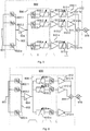
- Fig. 2 illustrates an embodiment of an analog front end arrangement 200 for multi-band reception of frequency bands for cellular communication which is suitable for operation between an antenna arrangement 220 and IF or baseband processing circuitry 230.
- the receiver front end arrangement 200 for multi-band reception of frequency bands for cellular communication.
- the receiver front end arrangement 200 comprises a radio frequency signal input suitable to be connected to the antenna arrangement 220, a filter bank 202 of non-overlapping band filters 202:1, 202:2, ..., 202:n associated with respective band n for the multi-band reception, a common low-noise amplifier 204 having its input connected to the outputs of respective band filters 202:1, 202:2, ..., 202:n of the filter bank 202, a signal conditioning arrangement 206 connected to the output of the common low-noise amplifier 204, wherein the signal conditioning arrangement 206 comprises a path for each band of the bands of the multi-band reception, wherein each path comprises a band filter 208:1, 208:2, ..., 208:n and an attenuator 210:1, 210:2, ..., 210:n, a low-noise amplifier arrangement 212 connected to the signal conditioning arrangement 206 comprising a path for each band of bands of the multi-band reception which is connected to the corresponding path of the signal conditioning arrangement, and for
- the attenuators 210:1, 210:2, ..., 210:n are controllable such that levels of signals of respective path of the low-noise amplifier arrangement 212 is such that the signals of respective path of the low-noise amplifier arrangement 212 is suitable to be combined by the combiner structure 214. It is to be noted that the signal is not mixed until after the combiner structure 214 by a mixer arrangement 216, i.e. the signals at the output of the combiner structure 214 has the same frequencies as the corresponding signals at the radio signal input.
- the signal conditioning arrangement 206 is arranged to condition signals for respective path of the low-noise amplifier arrangement, which provides for proper combining by the combiner structure 214.
- the illustrations under the illustration of the front end arrangement 200 are schematic noise spectral density diagrams for the respective part of the front end arrangement 200 and will be further discussed with reference to Figs 3-6 .
- respective path of the signal conditioning arrangement are connected between corresponding path of the filter bank and the corresponding path of the low-noise amplifier arrangement such that for each band for the multi-band reception there is formed a path through the filter bank, the signal conditioning arrangement and the low-noise amplifier arrangement.
- the common low-noise amplifier 204 is omitted, and any amplification is performed by the low-noise amplifiers 212:1, 212:2, ..., 212:n of the low-noise amplifier arrangement 212.
- each path e.g. of the signal conditioning arrangement, comprises a variable gain amplifier, and the variable gain amplifiers are controllable such that levels of respective path of the low-noise amplifier arrangement is suitable to be combined by the combiner structure 214.
- the attenuators 210:1, 210:2, ..., 210:n may be omitted.
- the attenuators or variable gain amplifiers are controllable such that levels of signals of respective path of the low-noise amplifier arrangement provides a sufficient signal level without saturating elements of respective path of the low-noise amplifier arrangement.
- the output of the combiner structure 214 is arranged to be connected to the mixer arrangement 230.
- the respective band filters may comprise an electromechanical filter, e.g. a surface acoustic wave filter, a bulk acoustic wave filter, a garnet filter, etc.
- an electromechanical filter e.g. a surface acoustic wave filter, a bulk acoustic wave filter, a garnet filter, etc.
- the band filter may comprise a pass-band frequency range covering e.g. carriers to be received within the band, a fraction of the band or the entire band, whichever is found beneficiary for the bands at design of the filter structures.
- Fig. 3 illustrates an embodiment of an analog front end arrangement 300 for multi-band reception of frequency bands for cellular communication which is suitable for operation between an antenna arrangement and IF or baseband processing circuitry, which later elements are not shown in Fig. 3 .
- the noise after the low-noise amplifier (LNA) 204 is likely broadband since the input signal to the LNA 204 is collected from the multitude of bands and also the active circuit of the LNA contributes with thermal noise and noise form active components of the LNA over a broad band.
- the band filters also filters the noise, wherein any noise at the output of the respective band filters will be suppressed outside the pass bands of the filters.
- the signal is provided through the attenuators, they will introduce some broadband noise, e.g. thermal noise, which then is amplified by the low-noise amplifier arrangement 212.
- the front end circuit of Fig. 3 comprises a filter bank 302 comprising band filters 302:1, 302:2, ..., 302:n associated with respective band for the multi-band reception of n bands.
- the band filters are preferably non-overlapping in frequency band since the bands are reasonably distinct from each other.
- the outputs of the band filters 302:1, 302:2, ..., 302:n are combined and amplified by an LNA 304.
- the output from the LNA 304 is provided to a signal conditioning arrangement 306.
- LNA 304 it is not necessary to have a single common LNA 304; there may be two or more LNAs, or even one LNA for each band.
- a reason to have more than one LNA may be that the aggregate bandwidth of all the bands is too wide for designing a single efficient LNA that can handle all the bands. If more than one LNA is used, the combining and splitting demonstrated above will be adapted accordingly, or in the case for an LNA for each band, omitted.
- a benefit of using a single LNA 304 is that less circuit area may be used.
- the signal conditioning arrangement 306 comprises attenuators 310:1, 310:2, ..., 310:n.
- the signal input to the signal conditioning arrangement 306 is split and provided to respective band paths 1, 2, ..., n, and provided to the respective attenuator 310:1, 310:2, ..., 310:n.
- the outputs of the signal conditioning arrangement 306 are connected to a low-noise amplifier arrangement 312.
- the respective attenuator 310:1, 310:2, ..., 310:n of the signal conditioning arrangement 306 is connected to a respective, i.e. for each path, low-noise amplifier 312:1, 312:2, ..., 312:n.
- the respective low-noise amplifier 312:1, 312:2, ..., 312:n has band pass characteristics according to the respective associated band.
- each LNA 312:1, 312:2, ..., 312:n may have an integrated resonator or filter 313:1, 313:2, ..., 313:n for providing the band pass characteristics.
- the resonator or filter 313:1, 313:2, ..., 313:n is preferably controllable such that assignment of bands can be made for an implementation of a multi-band receiver.
- Each LNA 312:1, 312:2, ..., 312:n may comprise a first amplifier stage 312:1a, 312:2a, ..., 312:na, to which the resonator or filter 313:1, 313:2, ..., 313:n is a load, and a second amplifier stage 312:1b, 312:2b, ..., 312:nb which provides the output of the respective LNA 312:1, 312:2, ..., 312:n and also serve as a buffer and isolation stage prior combining of the band signals.
- the LNA arrangement 312 is connected to a combiner structure 314 arranged to combine the outputs of the respective low-noise amplifier 312:1, 312:2, ..., 312:n of the paths of the low-noise amplifier arrangement 312.
- the attenuators 310:1, 310:2, ..., 310:n are controllable such that levels of signals of respective path of the low-noise amplifier arrangement 312 make the signals suitable to be combined by the combiner structure 314. It is to be noted that the signal is not mixed until after the combiner structure 314 by a mixer arrangement 316, i.e. the signals at the output of the combiner structure 314 has the same frequencies as the corresponding signals at the radio signal input.
- the signal conditioning arrangement 306 is arranged to condition signals for respective path of the low-noise amplifier arrangement, which provides for proper combining by the combiner structure 314.
- each path e.g. of the signal conditioning arrangement 306, comprises a variable gain amplifier, and the variable gain amplifiers are controllable such that levels of signals of respective path of the low-noise amplifier arrangement make the signals suitable to be combined by the combiner.
- the attenuators 310:1, 310:2, ..., 310:n may be omitted.
- the noise after LNA 304 is likely broadband for the same reasons as demonstrated with reference to Fig. 2 .
- the signal is provided through the attenuators 310:1, 310:2, ..., 310:n, they will introduce some broadband noise, e.g.
- thermal noise which then is amplified by the first amplifier stage 312:1a, 312:2a, ..., 312:na of the low-noise amplifier arrangement 312.
- the resonators or filters 313:1, 313:2, ..., 313:n will apply the band pass characteristics also on the noise, wherein out-of-band noise at the input of the respective second amplifier stage 312:1b, 312:2b, ..., 312:nb will be suppressed outside the pass bands of the filters, and thus out-of-band noise from respective LNA 312:1, 312:2, ..., 312:n will be reduced before the combining in the combiner structure 314 such that such out-of-band noise will have limited impact on the signals for the other bands when combined. Receiver performance may thereby be improved.
- Fig. 4 illustrates an embodiment of an analog front end arrangement 400 for multi-band reception of frequency bands for cellular communication which is suitable for operation between an antenna arrangement and IF or baseband processing circuitry, which later elements are not shown in Fig. 4 .
- the front end arrangement 400 comprises a filter bank 402 comprising band filters 402:1, 402:2, ..., 402:n associated with respective band for the multi-band reception of n bands, and an LNA 404.
- the similar variations and features as demonstrated with reference to Fig. 3 are applicable also for the front end arrangement 400 of Fig. 4 .
- the output from the LNA 404 is provided to a signal conditioning arrangement 406.
- the signal conditioning arrangement 406 comprises variable gain amplifiers 410:1, 410:2, ..., 410:n and band filters 408:1, 408:2, ..., 408:n for respective band path 1, 2, ..., n.
- the signal input to the signal conditioning arrangement 406 is split and provided to the respective band paths 1, 2, ..., n, and provided to the respective variable gain amplifier 410:1, 410:2, ..., 410:n.
- the outputs of the variable gain amplifiers 410:1, 410:2, ..., 410:n are provided to the band filters 408:1, 408:2, ..., 408:n, respectively, wherein the outputs of the band filters 408:1, 408:2, ..., 408:n form the output of the signal conditioning arrangement 406.
- the outputs of the signal conditioning arrangement 406 are connected to a LNA arrangement 412.
- the respective band filter 408:1, 408:2, ..., 408:n of the signal conditioning arrangement 406 is thus connected to a respective, i.e. for each path, low-noise amplifier 412:1, 412:2, ..., 412:n.
- the LNA arrangement 412 is connected to a combiner structure 414 arranged to combine the outputs of the respective low-noise amplifier 412:1, 412:2, ..., 412:n of the paths of the LNA arrangement 412.
- variable gain amplifiers 410:1, 410:2, ..., 410:n are controllable such that levels of signals of respective path of the LNA arrangement 412 make the signals suitable to be combined by the combiner structure 414. It is to be noted that the signal is not mixed until after the combiner structure 414 by a mixer arrangement 416, i.e. the signals at the output of the combiner structure 414 has the same frequencies as the corresponding signals at the radio signal input.
- the signal conditioning arrangement 406 is arranged to condition signals for respective path of the low-noise amplifier arrangement, which provides for proper combining by the combiner structure 314.
- the noise after LNA 404 is likely broadband for the same reasons as demonstrated with reference to Fig. 2 .
- the signal is provided through the variable gain amplifiers 410:1, 410:2, ..., 410:n, they will, in addition to amplifying the broadband noise at their inputs, introduce some broadband noise, e.g. thermal noise.
- the band filters 408:1, 408:2, ..., 408:n will filter also the noise, wherein out-of-band noise at the input of the respective LNA 412:1, 412:2, ..., 412:n will be suppressed outside the pass bands of the filters, and thus out-of-band noise from respective LNA 412:1, 412:2, ..., 412:n will be reduced before the combining in the combiner structure 414 such that such out-of-band noise will have limited impact on the signals for the other bands when combined. Receiver performance may thereby be improved.
- FIG. 5 illustrates an embodiment of an analog front end arrangement 500 for multi-band reception of frequency bands for cellular communication
- a filter bank 502 with its band filters 502:1, 502:2, ..., 502:n, and a LNA 504 is similar to what has been demonstrated with reference to Figs 2 to 4
- a signal conditioning arrangement 506 is similar to the signal conditioning arrangement 206 of Fig. 2 , but here combined with a LNA arrangement 512 similar to the LNA arrangement 312 of Fig. 3 .
- the signal conditioning arrangement 506 comprises a path for each band of the bands of the multi-band reception, wherein each path comprises a band filter 508:1, 508:2, ..., 508:n and an attenuator 510:1, 510:2, ..., 510:n.
- the outputs of the signal conditioning arrangement 506 are connected to the LNA arrangement 512.
- the respective attenuator 510:1, 510:2, ..., 510:n of the signal conditioning arrangement 506 is connected to a respective, i.e. for each path, low-noise amplifier 512:1, 512:2, ..., 512:n.
- the respective low-noise amplifier 512:1, 512:2, ..., 512:n has band pass characteristics according to the respective associated band.
- each LNA 512:1, 512:2, ..., 512:n may have an integrated resonator or filter 513:1, 513:2, ..., 513:n for providing the band pass characteristics.
- the resonator or filter 513:1, 513:2, ..., 513:n is preferably controllable such that assignment of bands can be made dynamically.
- Each LNA 512:1, 512:2, ..., 512:n may comprise a first amplifier stage 512:1a, 512:2a, ..., 512:na, to which the resonator or filter 513:1, 513:2, ..., 513:n is a load, and a second amplifier stage 512:1b, 512:2b, ..., 512:nb which provides the output of the respective LNA 512:1, 512:2, ..., 512:n and also serve as a buffer and isolation stage prior combining of the band signals.
- the LNA arrangement 512 is connected to a combiner structure 514 arranged to combine the outputs of the respective low-noise amplifier 512:1, 512:2, ..., 512:n of the paths of the low-noise amplifier arrangement 512.
- the attenuators 510:1, 510:2, ..., 510:n are controllable such that levels of signals of respective path of LNA arrangement 512 make the signals suitable to be combined by a combiner structure 514. It is to be noted that the signal is not mixed until after the combiner structure 514 by a mixer arrangement 516, i.e. the signals at the output of the combiner structure 514 has the same frequencies as the corresponding signals at the radio signal input.
- the signal conditioning arrangement 506 is arranged to condition signals for respective path of the low-noise amplifier arrangement, which provides for proper combining by the combiner structure 514.
- each path e.g. of the signal conditioning arrangement 506, comprises a variable gain amplifier, and the variable gain amplifiers are controllable such that levels of signals of respective path of the low-noise amplifier arrangement make the signals suitable to be combined by the combiner.
- the attenuators 510:1, 510:2, ..., 510:n may be omitted.
- Out-of-band noise is reduced in a similar way as demonstrated for the front end arrangement 300 of Fig. 3 .
- FIG. 6 illustrates an embodiment of an analog front end arrangement 600 for multi-band reception of frequency bands for cellular communication where a filter bank 602, with its band filters 602:1, 602:2, ..., 602:n, and a LNA 604 is similar to what has been demonstrated with reference to Figs 2 to 5 .
- a signal conditioning arrangement 606 comprises attenuators 610:1, 610:2, ..., 610:n and band filters 608:1, 608:2, ..., 608:n for respective band path 1, 2, ..., n.
- the signal input to the signal conditioning arrangement 606 is split and provided to the respective band paths 1, 2, ..., n, and provided to the respective attenuator 610:1, 610:2, ..., 610:n.
- the outputs of the attenuators 610:1, 610:2, ..., 610:n are provided to the band filters 608:1, 608:2, ..., 608:n, respectively, wherein the outputs of the band filters 608:1, 608:2, ..., 608:n form the output of the signal conditioning arrangement 606.
- the outputs of the signal conditioning arrangement 606 are connected to a LNA arrangement 612.
- the respective band filter 608:1, 608:2, ..., 608:n of the signal conditioning arrangement 606 is thus connected to a respective, i.e. for each path, low-noise amplifier 612:1, 612:2, ..., 612:n.
- the LNA arrangement 612 is connected to a combiner structure 614 arranged to combine the outputs of the respective low-noise amplifier 612:1, 612:2, ..., 612:n of the paths of the LNA arrangement 612.
- the attenuators 610:1, 610:2, ..., 610:n are controllable such that levels of signals of respective path of the LNA arrangement 612 make the signals suitable to be combined by the combiner structure 614. It is to be noted that the signal is not mixed until after the combiner structure 614 by a mixer arrangement 616, i.e. the signals at the output of the combiner structure 614 has the same frequencies as the corresponding signals at the radio signal input.
- the signal conditioning arrangement 606 is arranged to condition signals for respective path of the low-noise amplifier arrangement, which provides for proper combining by the combiner structure 614.
- Out-of-band noise is reduced in a similar way as demonstrated for the front end arrangement 300 of Fig. 3 .
- the attenuators or variable gain amplifiers as demonstrated herein may also be controllable such that levels of respective path of the LNA arrangement further provides a sufficient signal level without saturating elements of respective path of the LNA arrangement.
- the circuitry of the front end arrangement is implemented on-chip except for the band filters, which may be implemented off-chip.
- LNAs (204, 304, 404, 504, 604 in Figs 2-6 ) and attenuators or variable gain amplifiers (310:1-n, 410:1-n, 610:1-n in Figs 3, 4 and 6 ) may be implemented on one chip using a first technology, e.g. using some high performance material such as a combination of elements from the third and fifth group of the periodic table, e.g.
- GaAs, GaN or InP, and LNAs 212:1-n, 312:1-n, 412:1-n, 512:1-n, 612:1-n in Figs 2-6 ), attenuators (210:1-n, 510:1-n in Figs 2 and 5 ), mixer (216, 316, 416, 516, 616 in Figs 2-6 ) and baseband circuitry may be implemented on a second chip using a second technology which enables a higher degree of integration, e.g. together with mixed signal and digital circuitry.
- the second technology may for example be CMOS or SiGe BiCMOS.
- the band filters concerned in this disclosure may for example comprise an electromechanical filter, for example a surface acoustic wave filter, a bulk acoustic wave filter or a garnet filter.
- the bands handled by the respective path as of this disclosure may be considered as a band of the multi-band reception, but may also be considered as a band having a pass-band frequency range covering carriers to be received within the band, a fraction of the band, or the entire band, i.e. as of given by frequency regulating authorities.
- the respective low-noise amplifier which has band pass characteristics, or which has a band filter connected, i.e. where the band filter output is directly connected to the input of the low-noise amplifier, provides for improved receiver performance, as demonstrated above with reference to some embodiments.
- a direct connection of band filters 408:1, 408:2, ..., 408:n, 608:1, 608:2, ..., 608:n to the LNAs 412:1, 412:2, ..., 412:n, 612:1, 612:2, ..., 612:n reasonably comprises some components, but may be implemented such that the input of the low-noise amplifier 412:1, 412:2, ..., 412:n, 612:1, 612:2, ..., 612:n is directly exposed to frequency and/or impedance characteristics of the band filter 408:1, 408:2, ..., 408:n , 608:1, 608:2, ..., 608:n.
- Examples of such components are a bond pad, a bond wire, a transmission line, a matching network with reactive components, an electrostatic discharge protection circuitry, a conductor on a printed circuit board, a chip carrier, a chip interposer, a chip package conductor lead, etc.
- Fig. 7 schematically illustrates a multi-band receiver 700 according to embodiments.
- the multi-band receiver 700 comprises a receiver front end 710 according to any of the embodiments demonstrated herein.
- the receiver front end 710 is suitable to be connected to an antenna arrangement 720.
- the multi-band receiver 700 further comprises a mixer arrangement 725, connected to the receiver front end 710, and a baseband arrangement 730 connected to the mixer arrangement 725.
- Fig. 8 schematically illustrates a base station 800 for operating as a radio network node in a cellular communication system.
- the base station 800 comprises a multi-band receiver 810 according to embodiments demonstrated above, for example such as the multi-band receiver 700 demonstrated with reference to Fig. 7 .
- the multi-band receiver 810 comprises a receiver front end 812 according to any of the embodiments demonstrated herein.
- the receiver front end 810 is suitable to be connected to an antenna arrangement 820.
- the multi-band receiver 810 further comprises a mixer arrangement, connected to the receiver front end 812, and a baseband arrangement 814 connected to the mixer arrangement.
- the base station 800 further comprises a transmitter 830.
- the transmitter comprises transmitter circuitry 832 suitable for modulation etc., and a transmitter power amplifier 834 which is connected to the antenna arrangement 820 for providing the signal to be transmitted.
- the base station 800 further comprises circuitry 840 for processing, logic, control, power supply, etc.
- the circuitry 840 is connected to the receiver 810 and the transmitter 830.
Landscapes
- Engineering & Computer Science (AREA)
- Computer Networks & Wireless Communication (AREA)
- Signal Processing (AREA)
- Input Circuits Of Receivers And Coupling Of Receivers And Audio Equipment (AREA)
- Amplifiers (AREA)
Claims (15)
- Agencement frontal de récepteur (300, 400, 500, 600) pour une réception multibande de bandes de fréquences pour une communication cellulaire, l'agencement frontal de récepteur (300, 400, 500, 600) comprenant :une entrée de signal radio fréquence (301, 401, 501, 601) apte à être connectée à un agencement d'antenne ;un banc de filtres (302, 402, 502, 602) de filtres de bande sans chevauchement (302:1-n, 402:1-n, 502:1-n, 602:1-n) associés à une bande respective pour la réception multibande ;un agencement de conditionnement de signaux (306, 406, 506, 606) connecté au banc de filtres (302, 402, 502, 602) ;un agencement d'amplificateur à faible bruit (312, 412, 512, 612) connecté à l'agencement de conditionnement de signaux (306, 406, 506, 606) comprenant un trajet pour chaque bande des bandes de la réception multibande, et pour chaque trajet associé à une bande pour la réception multibande, l'agencement d'amplificateur à faible bruit (312, 412, 512, 612) comprend un amplificateur à faible bruit (312:1-n, 412:1-n, 512:1-n, 612:1-n) dans lequel l'amplificateur à faible bruit respectif (312:1-n, 412:1-n, 512:1-n, 612:1-n) présente des caractéristiques passe-bande, ou présente un filtre de bande (408:1-n, 608:1-n) connecté, où la sortie de filtre de bande présente une connexion directe à l'entrée de l'amplificateur à faible bruit (312:1-n, 412:1-n, 512:1-n, 612:1-n), correspondant à une bande de la réception multibande, respectivement ; etune structure de combinaison (314, 414, 514, 614) agencée de manière à combiner les sorties de l'amplificateur à faible bruit respectif (312:1-n, 412:1-n, 512:1-n, 612:1-n) des trajets de l'agencement d'amplificateur à faible bruit (312, 412, 512, 612), dans lequel les signaux à la sortie de la structure de combinaison (314, 414, 514, 614) présentent les mêmes fréquences que les signaux correspondants à l'entrée de signal radio fréquence (301, 401, 501, 601);dans lequel l'agencement de conditionnement de signaux (306, 406, 506, 606) est agencé de manière à conditionner des signaux pour le trajet respectif de l'agencement d'amplificateur à faible bruit (312, 412, 512, 612).
- Agencement frontal de récepteur (300, 500, 600) selon la revendication 1, dans lequel l'agencement de conditionnement de signaux (306, 506, 606) comprend un trajet pour chaque bande des bandes de la réception multibande, dans lequel chaque trajet comprend un atténuateur (310:1-n, 510:1-n, 610:1-n), et dans lequel les atténuateurs (310:1-n, 510:1-n, 610:1-n) peuvent être commandés de sorte que des niveaux de signaux du trajet respectif de l'agencement d'amplificateur à faible bruit (312, 512, 612) sont tels que les signaux du trajet respectif de l'agencement d'amplificateur à faible bruit (312, 512, 612) sont aptes à être combinés par la structure de combinaison (314, 514, 614).
- Agencement frontal de récepteur selon la revendication 2, dans lequel un trajet respectif de l'agencement de conditionnement de signaux comprend un atténuateur connecté entre le trajet correspondant du banc de filtres et un étage d'amplificateur d'entrée du trajet correspondant de l'agencement d'amplificateur à faible bruit, de sorte que, pour chaque bande pour la réception multibande, est formé un trajet à travers le banc de filtres, l'agencement de conditionnement de signaux et l'agencement d'amplificateur à faible bruit.
- Agencement frontal de récepteur (300) selon la revendication 2, dans lequel l'agencement de conditionnement de signaux (306) comprend un amplificateur à faible bruit commun (304) dont l'entrée est connectée à chacune des sorties des filtres de bande (302:1-n) du banc de filtres (302) et dont la sortie est connectée à chaque entrée de chaque atténuateur (310:1-n) des trajets de l'agencement de conditionnement de signaux (306), dans lequel la sortie de chaque atténuateur (310:1-n) des trajets de l'agencement de conditionnement de signaux (306) est connectée à des entrées des trajets respectifs de l'agencement d'amplificateur à faible bruit (312).
- Agencement frontal de récepteur (400) selon la revendication 1, dans lequel l'agencement de conditionnement de signaux (406) comprend un trajet pour chaque bande des bandes de la réception multibande, dans lequel chaque trajet comprend un amplificateur à gain variable (410:1-n), et les amplificateurs à gain variable (410:1-n) peuvent être commandés de sorte que des niveaux de signaux du trajet respectif de l'agencement d'amplificateur à faible bruit (412) sont tels que les signaux du trajet respectif de l'agencement d'amplificateur à faible bruit (412) sont aptes à être combinés par la structure de combinaison (414).
- Agencement frontal de récepteur (400) selon la revendication 5, comprenant un amplificateur à faible bruit commun (404) dont l'entrée est connectée à chacune des sorties des filtres de bande (402:1-n) du banc de filtres (402), et dont la sortie est connectée à chaque entrée de chaque amplificateur à gain variable (410:1-n) des trajets de l'agencement de conditionnement de signaux (406), dans lequel la sortie de chaque amplificateur à gain variable (410:1-n) des trajets de l'agencement de conditionnement de signaux (406) est connectée à des entrées des trajets respectifs de l'agencement d'amplificateur à faible bruit (412).
- Agencement frontal de récepteur (300, 400, 500, 600) selon l'une quelconque des revendications 2 à 6, dans lequel les atténuateurs (310:1-n, 510:1-n, 610:1-n) ou les amplificateurs à gain variable (410:1-n) peuvent être commandés de sorte que des niveaux de signaux du trajet respectif de l'agencement d'amplificateur à faible bruit (412) fournissent en outre un niveau de signal suffisant sans saturer des éléments du trajet respectif de l'agencement d'amplificateur à faible bruit (412).
- Agencement frontal de récepteur (300, 400, 500, 600) selon l'une quelconque des revendications 1 à 7, dans lequel une sortie de la structure de combinaison (314, 414, 514, 614) est agencée de manière à être connectée à un agencement de mélangeur (316, 416, 516, 616).
- Agencement frontal de récepteur (300, 400, 500, 600) selon l'une quelconque des revendications 1 à 8, dans lequel les filtres de bande respectifs (302:1-n, 402:1-n, 502:1-n, 602:1-n) comprennent un filtre électromécanique comprenant l'un quelconque des filtres ci-dessous :un filtre à ondes acoustiques de surface ;un filtre à ondes acoustiques de masse ; etun filtre gyromagnétique.
- Agencement frontal de récepteur (400, 600) selon l'une quelconque des revendications 1 à 9, dans lequel la connexion directe comprend des composants tels que l'entrée de l'amplificateur à faible bruit est directement exposée à des caractéristiques de fréquence et/ou d'impédance du filtre de bande (408:1-n, 608:1-n).
- Agencement frontal de récepteur (400, 600) selon la revendication 10, dans lequel les composants comprennent un ou plusieurs des éléments suivants :un plot de connexion ;un fil de connexion ;une ligne de transmission ;un réseau d'adaptation avec des composants réactifs ;un circuit de protection contre les décharges électrostatiques ;un conducteur sur une carte de circuit imprimé ;un support de puce ;un élément d'interposition de puce ; etun fil conducteur de boîtier pavé.
- Agencement frontal de récepteur (300, 500) selon l'une quelconque des revendications 1 à 8, dans lequel l'amplificateur à faible bruit respectif (312:1-n, 512:1-n) de l'agencement d'amplificateur à faible bruit (312, 512) comprend un résonateur contrôlable intégré ou un filtre (313:1-n, 513:1-n) qui fournit des caractéristiques passe-bande de l'amplificateur à faible bruit respectif (312:1-n, 512:1-n).
- Agencement frontal de récepteur (300, 400, 500, 600) selon l'une quelconque des revendications 1 à 12, dans lequel l'amplificateur à faible bruit respectif (312:1-n, 512:1-n) qui présente des caractéristiques passe-bande, ou ledit filtre de bande respectif (412:1-n, 612:1-n) connecté à l'entrée de l'amplificateur à faible bruit (412:1-n, 612:1-n), comprend une plage de fréquences passe-bande couvrant l'une parmi :des porteuses à recevoir dans la bande ;une fraction de la bande ; etla bande entière.
- Récepteur multibande (700) comprenant
un agencement frontal de récepteur (300, 400, 500, 600, 710) selon l'une quelconque des revendications 1 à 13, apte à pour être connecté à un agencement d'antenne (720) ;
un agencement de mélangeur (725) connecté à l'agencement frontal de récepteur (710) ; et
un agencement de bande de base (730) connecté à l'agencement de mélangeur (725). - Station de base (800) destinée à fonctionner en tant qu'un noeud de réseau radio dans un système de communication cellulaire, dans laquelle la station de base (800) comprend un récepteur multibande (700, 810) selon la revendication 14.
Applications Claiming Priority (1)
| Application Number | Priority Date | Filing Date | Title |
|---|---|---|---|
| PCT/EP2014/055881 WO2015144206A1 (fr) | 2014-03-24 | 2014-03-24 | Dispositif frontal de récepteur, récepteur multi-bande et station de base |
Publications (2)
| Publication Number | Publication Date |
|---|---|
| EP3123616A1 EP3123616A1 (fr) | 2017-02-01 |
| EP3123616B1 true EP3123616B1 (fr) | 2018-08-22 |
Family
ID=50424216
Family Applications (1)
| Application Number | Title | Priority Date | Filing Date |
|---|---|---|---|
| EP14714638.5A Active EP3123616B1 (fr) | 2014-03-24 | 2014-03-24 | Dispositif frontal de récepteur, récepteur multi-bande et station de base |
Country Status (3)
| Country | Link |
|---|---|
| US (1) | US9998152B2 (fr) |
| EP (1) | EP3123616B1 (fr) |
| WO (1) | WO2015144206A1 (fr) |
Families Citing this family (3)
| Publication number | Priority date | Publication date | Assignee | Title |
|---|---|---|---|---|
| US9838056B2 (en) * | 2015-05-28 | 2017-12-05 | Skyworks Solutions, Inc. | Integrous signal combiner |
| KR20170004735A (ko) * | 2015-07-03 | 2017-01-11 | 삼성전자주식회사 | 전자 장치 및 그의 수신 방법 |
| CN112615631B (zh) * | 2020-12-18 | 2022-06-07 | 维沃移动通信有限公司 | 射频接收电路、射频信号接收方法、装置和电子设备 |
Family Cites Families (22)
| Publication number | Priority date | Publication date | Assignee | Title |
|---|---|---|---|---|
| US5966646A (en) | 1997-05-13 | 1999-10-12 | Ericsson, Inc. | Dual-band radio receiver |
| IT1316025B1 (it) * | 2000-12-15 | 2003-03-26 | Micron Technology Inc | Sistema di integrazione di dispositivi di memoria e logici. |
| US20060009979A1 (en) * | 2004-05-14 | 2006-01-12 | Mchale Mike | Vocal training system and method with flexible performance evaluation criteria |
| US20080304466A1 (en) * | 2007-06-06 | 2008-12-11 | Anchor Audio, Inc. | Wireless multipoint voice network |
| US7590396B2 (en) | 2005-10-06 | 2009-09-15 | Broadcom Corporation | Multimode communication device with shared signal path programmable filter |
| DE602005018492D1 (de) | 2005-11-03 | 2010-02-04 | Qualcomm Inc | Mehrbandempfänger für Signale von Navigationssatelliten (GNSS) |
| US20070298838A1 (en) * | 2006-06-22 | 2007-12-27 | Honeywell International Inc. | Apparatus and method for improving reception in a system with multiple transmitters and receivers operating on a single antenna |
| US8088126B2 (en) * | 2006-08-17 | 2012-01-03 | Fugo Richard J | Method and apparatus for plasma incision of cardiovascular tissue |
| US7715813B2 (en) | 2007-01-15 | 2010-05-11 | Mediatek Singapore Pte Ltd | Receiver having tunable amplifier with integrated tracking filter |
| US8412142B2 (en) * | 2009-04-09 | 2013-04-02 | Broadcom Corporation | Multiple frequency band information signal universal front end with adjustable ADC(s) |
| US8576768B2 (en) | 2009-04-16 | 2013-11-05 | Qualcomm Incorporated | Hybrid multi-band receiver |
| US8260224B2 (en) * | 2009-12-02 | 2012-09-04 | Sige Semiconductor Inc. | System and method of prebias for rapid power amplifier response correction |
| DE102010001147B4 (de) | 2010-01-22 | 2016-11-17 | Fraunhofer-Gesellschaft zur Förderung der angewandten Forschung e.V. | Mehrfrequenzbandempfänger auf Basis von Pfadüberlagerung mit Regelungsmöglichkeiten |
| US8427366B2 (en) * | 2010-07-27 | 2013-04-23 | Texas Instruments Incorporated | Dual frequency receiver with single I/Q IF pair and mixer |
| US9252827B2 (en) | 2011-06-27 | 2016-02-02 | Qualcomm Incorporated | Signal splitting carrier aggregation receiver architecture |
| US12081243B2 (en) * | 2011-08-16 | 2024-09-03 | Qualcomm Incorporated | Low noise amplifiers with combined outputs |
| CA2855344A1 (fr) * | 2011-11-09 | 2013-05-16 | Aurora Networks, Inc. | Emetteur optique analogique enfichable a faible rapport geometrique et module hote |
| EP2615764A3 (fr) | 2011-11-30 | 2014-04-09 | Sequans Communications Limited | Appareil pour agrégation de porteuses |
| US9203451B2 (en) | 2011-12-14 | 2015-12-01 | Infineon Technologies Ag | System and method for an RF receiver |
| WO2013093969A1 (fr) * | 2011-12-21 | 2013-06-27 | 三菱電機株式会社 | Appareil de communication sans fil |
| US8717095B2 (en) * | 2012-07-09 | 2014-05-06 | Siemens Energy, Inc. | Chopper circuitry operable in a high temperature environment of a turbine engine |
| US9190957B2 (en) * | 2013-06-18 | 2015-11-17 | Silicon Laboratories Inc. | Efficient dual channel conversion in a multi-band radio receiver |
-
2014
- 2014-03-24 EP EP14714638.5A patent/EP3123616B1/fr active Active
- 2014-03-24 WO PCT/EP2014/055881 patent/WO2015144206A1/fr not_active Ceased
- 2014-03-24 US US15/127,028 patent/US9998152B2/en active Active
Non-Patent Citations (1)
| Title |
|---|
| None * |
Also Published As
| Publication number | Publication date |
|---|---|
| EP3123616A1 (fr) | 2017-02-01 |
| WO2015144206A1 (fr) | 2015-10-01 |
| US20170111063A1 (en) | 2017-04-20 |
| US9998152B2 (en) | 2018-06-12 |
Similar Documents
| Publication | Publication Date | Title |
|---|---|---|
| US6567648B1 (en) | System combining radio frequency transmitter and receiver using circulator and method for canceling transmission signal thereof | |
| KR102507772B1 (ko) | 무결 신호 결합기 | |
| US9973159B1 (en) | Multimode multiband wireless device with broadband power amplifier | |
| CN101594164B (zh) | 无线通信设备、无线通信方法、天线设备以及第一双工器 | |
| US10153797B2 (en) | Communication module | |
| KR102140190B1 (ko) | 스위칭 유닛을 구비한 디바이스 및 그 애플리케이션 | |
| US11265037B2 (en) | Radio frequency circuit and communication device | |
| CN111756386B (zh) | 前端电路以及通信装置 | |
| US9020449B2 (en) | Software-defined radio with broadband amplifiers and antenna matching | |
| JP2006166277A (ja) | 送受信装置およびモジュール | |
| US10505702B2 (en) | Transmission/reception module | |
| US10965325B2 (en) | Communication unit | |
| US20210314010A1 (en) | Radio-frequency module and communication device | |
| US20170054485A1 (en) | Filter module supporting carrier aggregation and electronic device including the same | |
| US9998152B2 (en) | Receiver front end arrangement, multi-band receiver and base station | |
| US10211879B2 (en) | Front-end module | |
| WO2019244757A1 (fr) | Circuit d'amplification à haute fréquence et dispositif de communication | |
| CN115250095A (zh) | 功率放大模块 | |
| US6952566B2 (en) | Transmission circuit and unnecessary radiant wave suppression method | |
| US10333481B2 (en) | Amplification apparatus having single-input multi-output structure | |
| WO2023195263A1 (fr) | Circuit haute fréquence et dispositif de communication |
Legal Events
| Date | Code | Title | Description |
|---|---|---|---|
| STAA | Information on the status of an ep patent application or granted ep patent |
Free format text: STATUS: THE INTERNATIONAL PUBLICATION HAS BEEN MADE |
|
| PUAI | Public reference made under article 153(3) epc to a published international application that has entered the european phase |
Free format text: ORIGINAL CODE: 0009012 |
|
| STAA | Information on the status of an ep patent application or granted ep patent |
Free format text: STATUS: REQUEST FOR EXAMINATION WAS MADE |
|
| 17P | Request for examination filed |
Effective date: 20161019 |
|
| AK | Designated contracting states |
Kind code of ref document: A1 Designated state(s): AL AT BE BG CH CY CZ DE DK EE ES FI FR GB GR HR HU IE IS IT LI LT LU LV MC MK MT NL NO PL PT RO RS SE SI SK SM TR |
|
| AX | Request for extension of the european patent |
Extension state: BA ME |
|
| DAX | Request for extension of the european patent (deleted) | ||
| GRAP | Despatch of communication of intention to grant a patent |
Free format text: ORIGINAL CODE: EPIDOSNIGR1 |
|
| STAA | Information on the status of an ep patent application or granted ep patent |
Free format text: STATUS: GRANT OF PATENT IS INTENDED |
|
| INTG | Intention to grant announced |
Effective date: 20180517 |
|
| GRAS | Grant fee paid |
Free format text: ORIGINAL CODE: EPIDOSNIGR3 |
|
| GRAA | (expected) grant |
Free format text: ORIGINAL CODE: 0009210 |
|
| STAA | Information on the status of an ep patent application or granted ep patent |
Free format text: STATUS: THE PATENT HAS BEEN GRANTED |
|
| AK | Designated contracting states |
Kind code of ref document: B1 Designated state(s): AL AT BE BG CH CY CZ DE DK EE ES FI FR GB GR HR HU IE IS IT LI LT LU LV MC MK MT NL NO PL PT RO RS SE SI SK SM TR |
|
| REG | Reference to a national code |
Ref country code: GB Ref legal event code: FG4D |
|
| REG | Reference to a national code |
Ref country code: CH Ref legal event code: EP |
|
| REG | Reference to a national code |
Ref country code: AT Ref legal event code: REF Ref document number: 1033659 Country of ref document: AT Kind code of ref document: T Effective date: 20180915 |
|
| REG | Reference to a national code |
Ref country code: IE Ref legal event code: FG4D |
|
| REG | Reference to a national code |
Ref country code: DE Ref legal event code: R096 Ref document number: 602014030829 Country of ref document: DE |
|
| REG | Reference to a national code |
Ref country code: NL Ref legal event code: FP |
|
| REG | Reference to a national code |
Ref country code: LT Ref legal event code: MG4D |
|
| PG25 | Lapsed in a contracting state [announced via postgrant information from national office to epo] |
Ref country code: IS Free format text: LAPSE BECAUSE OF FAILURE TO SUBMIT A TRANSLATION OF THE DESCRIPTION OR TO PAY THE FEE WITHIN THE PRESCRIBED TIME-LIMIT Effective date: 20181222 Ref country code: BG Free format text: LAPSE BECAUSE OF FAILURE TO SUBMIT A TRANSLATION OF THE DESCRIPTION OR TO PAY THE FEE WITHIN THE PRESCRIBED TIME-LIMIT Effective date: 20181122 Ref country code: LT Free format text: LAPSE BECAUSE OF FAILURE TO SUBMIT A TRANSLATION OF THE DESCRIPTION OR TO PAY THE FEE WITHIN THE PRESCRIBED TIME-LIMIT Effective date: 20180822 Ref country code: SE Free format text: LAPSE BECAUSE OF FAILURE TO SUBMIT A TRANSLATION OF THE DESCRIPTION OR TO PAY THE FEE WITHIN THE PRESCRIBED TIME-LIMIT Effective date: 20180822 Ref country code: NO Free format text: LAPSE BECAUSE OF FAILURE TO SUBMIT A TRANSLATION OF THE DESCRIPTION OR TO PAY THE FEE WITHIN THE PRESCRIBED TIME-LIMIT Effective date: 20181122 Ref country code: RS Free format text: LAPSE BECAUSE OF FAILURE TO SUBMIT A TRANSLATION OF THE DESCRIPTION OR TO PAY THE FEE WITHIN THE PRESCRIBED TIME-LIMIT Effective date: 20180822 Ref country code: GR Free format text: LAPSE BECAUSE OF FAILURE TO SUBMIT A TRANSLATION OF THE DESCRIPTION OR TO PAY THE FEE WITHIN THE PRESCRIBED TIME-LIMIT Effective date: 20181123 Ref country code: FI Free format text: LAPSE BECAUSE OF FAILURE TO SUBMIT A TRANSLATION OF THE DESCRIPTION OR TO PAY THE FEE WITHIN THE PRESCRIBED TIME-LIMIT Effective date: 20180822 |
|
| REG | Reference to a national code |
Ref country code: AT Ref legal event code: MK05 Ref document number: 1033659 Country of ref document: AT Kind code of ref document: T Effective date: 20180822 |
|
| PG25 | Lapsed in a contracting state [announced via postgrant information from national office to epo] |
Ref country code: HR Free format text: LAPSE BECAUSE OF FAILURE TO SUBMIT A TRANSLATION OF THE DESCRIPTION OR TO PAY THE FEE WITHIN THE PRESCRIBED TIME-LIMIT Effective date: 20180822 Ref country code: AL Free format text: LAPSE BECAUSE OF FAILURE TO SUBMIT A TRANSLATION OF THE DESCRIPTION OR TO PAY THE FEE WITHIN THE PRESCRIBED TIME-LIMIT Effective date: 20180822 Ref country code: LV Free format text: LAPSE BECAUSE OF FAILURE TO SUBMIT A TRANSLATION OF THE DESCRIPTION OR TO PAY THE FEE WITHIN THE PRESCRIBED TIME-LIMIT Effective date: 20180822 |
|
| PG25 | Lapsed in a contracting state [announced via postgrant information from national office to epo] |
Ref country code: CZ Free format text: LAPSE BECAUSE OF FAILURE TO SUBMIT A TRANSLATION OF THE DESCRIPTION OR TO PAY THE FEE WITHIN THE PRESCRIBED TIME-LIMIT Effective date: 20180822 Ref country code: RO Free format text: LAPSE BECAUSE OF FAILURE TO SUBMIT A TRANSLATION OF THE DESCRIPTION OR TO PAY THE FEE WITHIN THE PRESCRIBED TIME-LIMIT Effective date: 20180822 Ref country code: IT Free format text: LAPSE BECAUSE OF FAILURE TO SUBMIT A TRANSLATION OF THE DESCRIPTION OR TO PAY THE FEE WITHIN THE PRESCRIBED TIME-LIMIT Effective date: 20180822 Ref country code: PL Free format text: LAPSE BECAUSE OF FAILURE TO SUBMIT A TRANSLATION OF THE DESCRIPTION OR TO PAY THE FEE WITHIN THE PRESCRIBED TIME-LIMIT Effective date: 20180822 Ref country code: EE Free format text: LAPSE BECAUSE OF FAILURE TO SUBMIT A TRANSLATION OF THE DESCRIPTION OR TO PAY THE FEE WITHIN THE PRESCRIBED TIME-LIMIT Effective date: 20180822 Ref country code: AT Free format text: LAPSE BECAUSE OF FAILURE TO SUBMIT A TRANSLATION OF THE DESCRIPTION OR TO PAY THE FEE WITHIN THE PRESCRIBED TIME-LIMIT Effective date: 20180822 Ref country code: ES Free format text: LAPSE BECAUSE OF FAILURE TO SUBMIT A TRANSLATION OF THE DESCRIPTION OR TO PAY THE FEE WITHIN THE PRESCRIBED TIME-LIMIT Effective date: 20180822 |
|
| REG | Reference to a national code |
Ref country code: DE Ref legal event code: R097 Ref document number: 602014030829 Country of ref document: DE |
|
| PG25 | Lapsed in a contracting state [announced via postgrant information from national office to epo] |
Ref country code: SK Free format text: LAPSE BECAUSE OF FAILURE TO SUBMIT A TRANSLATION OF THE DESCRIPTION OR TO PAY THE FEE WITHIN THE PRESCRIBED TIME-LIMIT Effective date: 20180822 Ref country code: SM Free format text: LAPSE BECAUSE OF FAILURE TO SUBMIT A TRANSLATION OF THE DESCRIPTION OR TO PAY THE FEE WITHIN THE PRESCRIBED TIME-LIMIT Effective date: 20180822 Ref country code: DK Free format text: LAPSE BECAUSE OF FAILURE TO SUBMIT A TRANSLATION OF THE DESCRIPTION OR TO PAY THE FEE WITHIN THE PRESCRIBED TIME-LIMIT Effective date: 20180822 |
|
| PLBE | No opposition filed within time limit |
Free format text: ORIGINAL CODE: 0009261 |
|
| STAA | Information on the status of an ep patent application or granted ep patent |
Free format text: STATUS: NO OPPOSITION FILED WITHIN TIME LIMIT |
|
| 26N | No opposition filed |
Effective date: 20190523 |
|
| PG25 | Lapsed in a contracting state [announced via postgrant information from national office to epo] |
Ref country code: SI Free format text: LAPSE BECAUSE OF FAILURE TO SUBMIT A TRANSLATION OF THE DESCRIPTION OR TO PAY THE FEE WITHIN THE PRESCRIBED TIME-LIMIT Effective date: 20180822 |
|
| PG25 | Lapsed in a contracting state [announced via postgrant information from national office to epo] |
Ref country code: MC Free format text: LAPSE BECAUSE OF FAILURE TO SUBMIT A TRANSLATION OF THE DESCRIPTION OR TO PAY THE FEE WITHIN THE PRESCRIBED TIME-LIMIT Effective date: 20180822 |
|
| REG | Reference to a national code |
Ref country code: CH Ref legal event code: PL |
|
| PG25 | Lapsed in a contracting state [announced via postgrant information from national office to epo] |
Ref country code: LU Free format text: LAPSE BECAUSE OF NON-PAYMENT OF DUE FEES Effective date: 20190324 |
|
| REG | Reference to a national code |
Ref country code: BE Ref legal event code: MM Effective date: 20190331 |
|
| PG25 | Lapsed in a contracting state [announced via postgrant information from national office to epo] |
Ref country code: IE Free format text: LAPSE BECAUSE OF NON-PAYMENT OF DUE FEES Effective date: 20190324 Ref country code: LI Free format text: LAPSE BECAUSE OF NON-PAYMENT OF DUE FEES Effective date: 20190331 Ref country code: CH Free format text: LAPSE BECAUSE OF NON-PAYMENT OF DUE FEES Effective date: 20190331 |
|
| PG25 | Lapsed in a contracting state [announced via postgrant information from national office to epo] |
Ref country code: BE Free format text: LAPSE BECAUSE OF NON-PAYMENT OF DUE FEES Effective date: 20190331 Ref country code: FR Free format text: LAPSE BECAUSE OF NON-PAYMENT OF DUE FEES Effective date: 20190331 |
|
| PG25 | Lapsed in a contracting state [announced via postgrant information from national office to epo] |
Ref country code: TR Free format text: LAPSE BECAUSE OF FAILURE TO SUBMIT A TRANSLATION OF THE DESCRIPTION OR TO PAY THE FEE WITHIN THE PRESCRIBED TIME-LIMIT Effective date: 20180822 |
|
| PG25 | Lapsed in a contracting state [announced via postgrant information from national office to epo] |
Ref country code: MT Free format text: LAPSE BECAUSE OF NON-PAYMENT OF DUE FEES Effective date: 20190324 Ref country code: PT Free format text: LAPSE BECAUSE OF FAILURE TO SUBMIT A TRANSLATION OF THE DESCRIPTION OR TO PAY THE FEE WITHIN THE PRESCRIBED TIME-LIMIT Effective date: 20181222 |
|
| PG25 | Lapsed in a contracting state [announced via postgrant information from national office to epo] |
Ref country code: CY Free format text: LAPSE BECAUSE OF FAILURE TO SUBMIT A TRANSLATION OF THE DESCRIPTION OR TO PAY THE FEE WITHIN THE PRESCRIBED TIME-LIMIT Effective date: 20180822 |
|
| PG25 | Lapsed in a contracting state [announced via postgrant information from national office to epo] |
Ref country code: HU Free format text: LAPSE BECAUSE OF FAILURE TO SUBMIT A TRANSLATION OF THE DESCRIPTION OR TO PAY THE FEE WITHIN THE PRESCRIBED TIME-LIMIT; INVALID AB INITIO Effective date: 20140324 |
|
| PG25 | Lapsed in a contracting state [announced via postgrant information from national office to epo] |
Ref country code: MK Free format text: LAPSE BECAUSE OF FAILURE TO SUBMIT A TRANSLATION OF THE DESCRIPTION OR TO PAY THE FEE WITHIN THE PRESCRIBED TIME-LIMIT Effective date: 20180822 |
|
| PGFP | Annual fee paid to national office [announced via postgrant information from national office to epo] |
Ref country code: GB Payment date: 20260327 Year of fee payment: 13 |
|
| PGFP | Annual fee paid to national office [announced via postgrant information from national office to epo] |
Ref country code: DE Payment date: 20260327 Year of fee payment: 13 |
|
| PGFP | Annual fee paid to national office [announced via postgrant information from national office to epo] |
Ref country code: NL Payment date: 20260326 Year of fee payment: 13 |