EP3123976B1 - Appareil de durcissement à la lumiere - Google Patents
Appareil de durcissement à la lumiere Download PDFInfo
- Publication number
- EP3123976B1 EP3123976B1 EP15179313.0A EP15179313A EP3123976B1 EP 3123976 B1 EP3123976 B1 EP 3123976B1 EP 15179313 A EP15179313 A EP 15179313A EP 3123976 B1 EP3123976 B1 EP 3123976B1
- Authority
- EP
- European Patent Office
- Prior art keywords
- light
- curing device
- reflector
- led chips
- reflector body
- Prior art date
- Legal status (The legal status is an assumption and is not a legal conclusion. Google has not performed a legal analysis and makes no representation as to the accuracy of the status listed.)
- Active
Links
Images
Classifications
-
- A—HUMAN NECESSITIES
- A61—MEDICAL OR VETERINARY SCIENCE; HYGIENE
- A61C—DENTISTRY; APPARATUS OR METHODS FOR ORAL OR DENTAL HYGIENE
- A61C19/00—Dental auxiliary appliances
- A61C19/003—Apparatus for curing resins by radiation
Definitions
- the invention relates to a light curing device according to the preamble of claim 1.
- Such a light curing device is from the EP 2 332 490 known.
- a substrate is provided as the basis for the reception of LED chips. This is used for heat dissipation, but also for making electrical connections with the LED chips.
- Each chip has a reflection element which, in a manner known per se, extends from the chip in the direction of the light emission.
- the chips heat up when there is light emission, which is associated with heat emission, and thus also the reflector bodies.
- An expansion gap between the individual reflection elements of the reflectors makes it possible for them to expand symmetrically.
- reflector bodies have also been proposed which extend in a hexagonal arrangement to one another in order to achieve as dense a light emission as possible; in the case of such a light curing device, the arrangement of the chips is first mounted, and then the reflector body is attached to it in one go.
- the invention has for its object to provide a light curing device according to the preamble of claim 1, which is further improved in terms of flexibility with lower manufacturing costs, but at least the same optical quality.
- the special feature according to the invention is connected to the reinforcement walls or a reinforcement ring which surround a common reflector body with reflection elements.
- the reflection elements themselves are closely adjacent; they can even cut themselves.
- the ring-shaped, in particular circular, reinforcement wall effectively prevents the reflection elements from "moving apart” when heated and their optical axes shifting outwards.
- the reinforcement wall is on the one hand quite far away from the heat source LED chip, and on the other hand it extends diagonally upwards into the room, so that there is also a certain cooling there.
- the game slots according to the EP 2 332 491 can be avoided without sacrificing quality, and production is significantly more cost-effective, since instead of three injection molded parts, only one injection molded part has to be produced.
- sensors can also be accommodated particularly cheaply in the reflector body, namely on the outer corners of the partition walls or between them and the reinforcement wall.
- a three-leaf clover shape or a four-leaf clover shape is chosen for the arrangement of the reflection elements - there is always sufficient free space in front, and the sensor openings provided between the reinforcement wall and the clover leaf also allow air to pass through, which contributes to further cooling of the reinforcement wall.
- the reinforcement wall could also be referred to as a reinforcement ring, which preferably ends with the upper level of the reflectors.
- the ring-shaped design with a significantly reduced overall height compared to the partition walls also permits a further thermal separation from the substrate and the LED chips as heat sources.
- the reflector body according to the invention can be manufactured comparatively inexpensively and can be mirrored on the inside in a manner known per se after completion of the injection molding process. It is also flexible, because the recesses provided in an inexpensive version allow, for example, only two opposing reflectors to be fitted with LED chips. A third LED chip can be added in the case of higher power, and a fourth one in the case of further increased power, for example with a different emission wavelength.
- a central LED chip is added, that is to say in the center of the cloverleaf, below a corresponding passage recess.
- This LED chip emits with an emission maximum that is different from the emission maximum of the other LED chips.
- sensors are then provided below the indentations of the cloverleaf. These serve to detect radiation reflected from the dental restoration part to be hardened or from other objects in order to influence the control of the light hardening device overall in a favorable manner.
- a four-leaf clover can therefore accommodate, for example, three LED chips that emit with high power and an emission maximum that is in the blue light range, another LED chip in the fourth leaf of the clover that also emits with great power with a violet emission maximum , and a fifth LED chip in the central opening, which emits in a green emission maximum with lower power.
- the solution according to the invention with the special reflector body represents a flexible and inexpensive reflector body suitable for different light curing devices.
- converging lenses are provided in each reflector or at least one of the reflectors, each of which covers the LED chips.
- the converging lenses can be implemented in such a way that they are already mounted on the printed circuit board together with the associated LED chips and also lie on the printed circuit board over a large area surrounding the LED chip. The converging lens then becomes comparatively hot, even if it is made of plastic.
- the converging lens is separated from the associated reflector by a gap, which further contributes to the reflector being deformed only slightly,
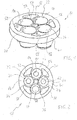
- the in Fig. 1 The reflector body 10 shown is part of a light curing device, which is otherwise not shown.
- the reflector body 10 is preferably made of black plastic and on the inside of the reflection elements is provided with an HR layer with a high reflection efficiency.
- the HR layer is matched to the emitted wavelength.
- the reflector body 10 is located at the interface between light sources and a light guide rod, as it looks better Fig. 3 can be seen in the handpiece of the light curing device.
- it is located at the tip of a rod, which is intended to be inserted into the mouth of a patient and emit light radiation there for hardening dental restorations, in front of the corresponding light sources which are mounted on the tip of the rod.
- the reflector body 10 is basically circular, that is to say from the outer shape, and in this respect extends around a central axis 12. It has a plurality of reflection elements, of which four reflection elements 14 to 20 are provided in the example. These extend in the manner of a four-leaf clover and end flush on a front surface 22. Together with associated ones Fig. 1 Collective lenses (not visible) each reflection element 14 to 20 forms a reflector, which is referred to here as an example reflector 24.
- the reflection elements 14 to 20 and thus the associated reflectors 20, 22, 24 are evenly distributed in the end view, which is also the case Fig. 2 is to be referenced, which shows the front view of the reflector body 10.
- the reflectors and the associated reflection elements generally adjoin one another, but are each separated from one another by partitions 30, 32, 34 and 36. This means that the cones do not intersect, but are closely adjacent. In particular, the distance is significantly less than the diameter of each cone on the front surface 22.
- all reflectors and reflection elements are part of the common reflector body. This is surrounded by a reinforcement ring 40, which could also be viewed as a reinforcement wall.
- the reinforcement ring 40 runs in a circular shape around all reflection elements 14 to 20 and, in this respect, borders on the outside thereof.
- the thickness of the reinforcement ring viewed in the radial direction is significantly more than the thickness of the partition walls 30 to 36, for example five times. It is also between 50% and 100% of the radius of a reflection element and therefore represents a solid ring which, even when the "inner life" of the reflector is deformed, keeps it stable on the outside.
- the reinforcement ring 40 accordingly stiffens the thin-walled reflection element arrangement in such a way that the optical axes of the reflection elements do not diverge from one another even when the reflection elements are heated.
- a central opening 50 is provided which extends in the "center" of the cloverleaf around the central axis 12. This opening serves to allow light to pass through a central LED chip, which can have an emission maximum in the green wavelength range.
- the secondary wavelength range can be purposefully and favorably green and can be used to determine the position of the light curing device as a function of the reflection result on a surface of a dental restoration.
- Openings 52, 54, 56 and 58 are provided along the outer circumference of the reflector body 10, but within the reinforcement ring 40 to allow light to pass through to the sensors.
- the openings 52 to 58 show that 1 and 2 apparent special shape, which is based on the outer circumference of the reflection elements on the one hand and on the inner circumference of the reinforcing ring 40 on the other.
- the reinforcement ring 40 is absent in the area of the openings 52 to 58, so that there are a plurality of reinforcement walls 40 on the reflection elements 14 to 20 and, instead of the openings, indentations with the same shape are provided.
- converging lenses 60, 62 and 64 can be arranged in front of three LED chips in the associated reflection elements 14, 16 and 20, which are quite compact and extend in front of LED chips which emit in the main wavelength range with a blue emission maximum.
- the fourth LED chip emits in a wavelength range with an emission maximum that is in the violet wavelength range and is covered by a converging lens 66.
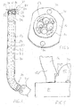
- Fig. 3 the manner in which a light guide rod 70 extends in front of the light source 72, which has LED chips 74 and 76, among other things, can be seen.
- the light source 72 also includes the central LED chip 78 which extends in the middle of the cloverleaf arrangement.
- the LED chips are arranged on a plated-through printed circuit board 80.
- the printed circuit board 80 has a high copper content and thick vias, so that the heat can be dissipated well to a heat sink, not shown.
- Sensors are arranged on the outer circumference of the region of the light source 72, two sensors 82 and 84 of which Fig. 3 are evident.
- the sensors extend behind the openings 52 and 56.
- the LED chips 74 to 78 emit transmission light 89 to the distal end 88 of the light guide rod 70. There, the emitted light leaves the light guide rod 70 and strikes a dental restoration part 90. There it is at least partially reflected. As reception light 92, it enters the light guide rod again and through openings 52 and 56 it falls on sensors 82 and 84, via which an evaluation takes place.
- a light mixing body 94 can be provided integrated in the light guide rod 70, which is arranged adjacent to the reflector body 10.
- Fig. 4 shows a perspective view of the printed circuit board 80 with mounted LED chips, sensors 82 and 84 and the reflector body 10.
- the printed circuit board 70 is securely fastened to the light curing device 80 via fastening holes 94.
- the light guide rod 70 is preferably detachably mounted in the rest of the light curing device. This is done by means of clamping fasteners known per se, but not shown here, so that the light guide rod, including the light mixing body, can be removed and, if necessary, autoclavable.
- FIG. 5 A part of a reflection element 14 is shown, in combination with the associated converging lens 60 and the associated LED chips 74. It can be seen that the reflector body 10 projects beyond the outer circumference of the collecting lens 60. However, a gap 100 is deliberately provided between the reflector body 14 and the converging lens 60, which in this respect offers thermal insulation. The heat given off by chip 74 is therefore predominantly dissipated via printed circuit board 80.
Landscapes
- Health & Medical Sciences (AREA)
- Oral & Maxillofacial Surgery (AREA)
- Dentistry (AREA)
- Epidemiology (AREA)
- Life Sciences & Earth Sciences (AREA)
- Animal Behavior & Ethology (AREA)
- General Health & Medical Sciences (AREA)
- Public Health (AREA)
- Veterinary Medicine (AREA)
- Led Device Packages (AREA)
Claims (16)
- Dispositif de photopolymérisation (80), avecune pluralité de puces LED individuels, dont chacun est associée à un réflecteur (24), où les puces LED (74, 76) sont disposées chacune à la même distance autour d'un axe central commun (12) et en particulier peuvent être commandées séparément, etdes éléments de réflexion (14, 16, 18, 20) des réflecteurs (24), qui sont disposés les uns à côté des autres, oùla distance entre chaque élément de réflexion (14, 16, 18, 20) est inférieure à un cinquième de leur diamètre respectif,les éléments de réflexion (14, 16, 18, 20) sont disposés en forme de trèfle autour de l'axe central commun (12) et font partie d'un corps réflecteur commun (10),le corps réflecteur présente une forme extérieure circulaire qui s'étend autour de l'axe central commun, et sépare les éléments de réflexion (14, 16, 18, 20) les uns des autres par des cloisons de séparation (30, 32, 34, 36), etle corps réflecteur (10) présente des cloisons de renforcement (40) à l'extérieur sur les éléments de réflexion (14, 16, 18, 20) qui se trouvent en face de l'axe central (12) par rapport à chacun des éléments réfléchissants (14, 16, 18, 20),caractérisé en ce quele corps réflecteur (10) présente une ouverture centrale (50) sous laquelle est disposée une puce LED (78) qui émet à un maximum d'émission qui est différent d'un maximum d'émission des autres puces LED.
- Dispositif de photopolymérisation selon la revendication 1, caractérisé en ce que le corps réflecteur (10) est relevé par rapport à un plan des puces LED (74, 76, 78) et des capteurs (82, 84) et est réalisé en une seule pièce.
- Dispositif de photopolymérisation selon la revendication 2, caractérisé en ce que les concavités ou ouvertures (52, 54, 56, 58) délimitent les cloisons de séparation (30, 32, 34, 36) vers l'extérieur, vues de dessus sur le corps réflecteur (10) du point de vue de l'axe central (12), où les cloisons de séparation (30, 32, 34, 36) et les concavités ou ouvertures (52, 54, 56, 58) sont disposées à symétrie ponctuelle par rapport à l'axe central (12).
- Dispositif de photopolymérisation selon l'une des revendications précédentes, caractérisé en ce que le corps réflecteur (10) présente une ouverture (50) en forme d'étoile dans la zone de l'axe central (12), où les cloisons de séparation (30-36) s'étendent radlalement à partir de l'ouverture (50) en forme d'étoile (50).
- Dispositif de photopolymérisation selon l'une des revendications précédentes, caractérisé en ce que le corps réflecteur (10) est monté sur un circuit Imprimé (80) par un nombre limité, en particulier trois, d'éléments de fixation qui pénètrent en particulier au moins partiellement le circuit imprimé (80).
- Dispositif de photopolymérisation selon l'une des revendications précédentes, caractérisé en ce que chaque puce LED (74, 76, 78) est recouverte d'une lentille collectrice qui s'étend autour de la puce sur un circuit imprimé (80) et est supportée sur celui-ci.
- Dispositif de photopolymérisation selon la revendication 6, caractérisé en ce que chaque lentille collectrice (60, 62, 64, 66) forme simultanément au moins une surface de guidage pour l'élément de friction (14, 16, 18, 20) du corps réflecteur (10) dans le réflecteur (24) associé.
- Dispositif de photopolymérisation selon la revendication 6 ou 7, caractérisé en ce que les lentilles collectrices (60, 62, 64) qui s'étendent devant des puces LED (74, 76, 78) qui émettent dans une plage de longueur d'onde principale avec un maximum d'émission bleu présentent un plus diamètre plus petit que la lentille convergente (66) qui s'étend devant une puce LED (74, 76, 78) qui émet dans une plage de longueur d'onde ayant un maximum d'émission situé dans la région de longueur d'onde violette.
- Dispositif de photopolymérisation selon l'une des revendications précédentes, caractérisé en ce que trois puces LED (74, 76, 78) sont disposées en triangle équilatéral l'une par rapport à l'autre, où l'une des puces LED (74, 76, 78) émet dans une plage de longueurs d'onde ayant un maximum d'émission située dans la plage dé longueurs d'onde violette et les deux autres puces LED (74, 76, 78) émettent dans une plage de longueurs d'onde principale avec un maximum d'émission bleu en particulier environ 470nm.
- Dispositif de photopolymérisation selon l'une des revendications précédentes, caractérisé en ce qu'un cloison de renforcement (40) présente une saillie de support qui s'étend vers l'extérieur depuis le cloison de renforcement (40), s'étend parallèlement à l'axe central (12) et est supportée sur le circuit Imprimé (80).
- Dispositif de photopolymérisation selon l'une des revendications 6 à 10, caractérisé en ce que chaque lentille collectrice. (60, 62, 64, 66) est séparée par un écart du réflecteur associé (24).
- Dispositif de photopolymérisation selon l'une des revendications 4 à 11, caractérisé en ce que dans la zone de l'axe central (12), le corps réflecteur (10) présente l'ouverture en étoile (50) sous laquelle est disposée une puce LED (78) ayant un spectre d'émission dans la plage des longueurs d'onde vertes.
- Dispositif de photopolymérisation selon l'une quelconque des revendications 1 à 8, caractérisé en ce que les puces LED (74, 76, 78) sont disposées sous les éléments de réflexion (14, 16, 18, 20), où celles-ci émettent de la lumière dans une gamme de longueurs d'onde allant du bleu au bleu clair, où trois puces LED (74, 76, 78) ayant un maximum d'émission à 470 nm et une puce LED ayant un maximum d'émission à 410nm sont prévues.
- Dispositif de photopolymérisation selon l'une des revendications précédentes, caractérisé en ce que des cloisons de réflexion, ayant une épaisseur de cloison uniforme, en particulier entre un vingtième et un sixième du diamètre du réflecteur à son extrémité supérieure, sont pourvus vers les ouvertures (52, 54, 56, 58) pour les capteurs (82,84).
- Dispositif de photopolymérisation selon la revendication 14, caractérisé en ce que le corps réflecteur (10) présente un cloison extérieur, essentiellement cylindrique, et dont l'épaisseur de cloison est supérieur à une épaisseur de cloison du cloison du réflecteur, qui entoure au moins partiellement les éléments de réflexion (14, 16, 18, 20).
- Dispositif de traitement de la lumière selon l'une des revendications précédentes, caractérisé en ce que le corps réflecteur (10) présente une surface plane et est relié sur une face inférieure avec une tige de guidage de lumière (70) directement ou par un élément de couplage optique.
Priority Applications (3)
| Application Number | Priority Date | Filing Date | Title |
|---|---|---|---|
| EP15179313.0A EP3123976B1 (fr) | 2015-07-31 | 2015-07-31 | Appareil de durcissement à la lumiere |
| PCT/EP2016/067665 WO2017021190A1 (fr) | 2015-07-31 | 2016-07-25 | Appareil de photodurcissement |
| US15/748,823 US10966808B2 (en) | 2015-07-31 | 2016-07-25 | Light-curing device |
Applications Claiming Priority (1)
| Application Number | Priority Date | Filing Date | Title |
|---|---|---|---|
| EP15179313.0A EP3123976B1 (fr) | 2015-07-31 | 2015-07-31 | Appareil de durcissement à la lumiere |
Publications (2)
| Publication Number | Publication Date |
|---|---|
| EP3123976A1 EP3123976A1 (fr) | 2017-02-01 |
| EP3123976B1 true EP3123976B1 (fr) | 2020-01-08 |
Family
ID=53785510
Family Applications (1)
| Application Number | Title | Priority Date | Filing Date |
|---|---|---|---|
| EP15179313.0A Active EP3123976B1 (fr) | 2015-07-31 | 2015-07-31 | Appareil de durcissement à la lumiere |
Country Status (3)
| Country | Link |
|---|---|
| US (1) | US10966808B2 (fr) |
| EP (1) | EP3123976B1 (fr) |
| WO (1) | WO2017021190A1 (fr) |
Family Cites Families (11)
| Publication number | Priority date | Publication date | Assignee | Title |
|---|---|---|---|---|
| US5420768A (en) * | 1993-09-13 | 1995-05-30 | Kennedy; John | Portable led photocuring device |
| US5660461A (en) * | 1994-12-08 | 1997-08-26 | Quantum Devices, Inc. | Arrays of optoelectronic devices and method of making same |
| US6200134B1 (en) * | 1998-01-20 | 2001-03-13 | Kerr Corporation | Apparatus and method for curing materials with radiation |
| US6331111B1 (en) * | 1999-09-24 | 2001-12-18 | Cao Group, Inc. | Curing light system useful for curing light activated composite materials |
| US6719558B2 (en) * | 1999-09-24 | 2004-04-13 | Densen Cao | Curing light |
| US7320593B2 (en) * | 2000-03-08 | 2008-01-22 | Tir Systems Ltd. | Light emitting diode light source for curing dental composites |
| WO2002033312A2 (fr) * | 2000-10-19 | 2002-04-25 | Reipur Technology A/S | Assemblage emetteur de rayonnement lumineux |
| DE10125341B4 (de) | 2001-05-23 | 2006-11-23 | Ivoclar Vivadent Ag | Bestrahlungsvorrichtung und Lichthärtgerät |
| US6866506B2 (en) * | 2001-05-23 | 2005-03-15 | Ivoclar Vivadent Ag | Light hardening apparatus particularly for a dental practice |
| JP2004267437A (ja) * | 2003-03-07 | 2004-09-30 | Morita Mfg Co Ltd | 歯科用ハンドピースの照明装置 |
| ES2648041T3 (es) | 2009-12-10 | 2017-12-28 | Ivoclar Vivadent Ag | Dispositivo de fotopolimerización para finalidades dentales |
-
2015
- 2015-07-31 EP EP15179313.0A patent/EP3123976B1/fr active Active
-
2016
- 2016-07-25 WO PCT/EP2016/067665 patent/WO2017021190A1/fr not_active Ceased
- 2016-07-25 US US15/748,823 patent/US10966808B2/en active Active
Non-Patent Citations (1)
| Title |
|---|
| None * |
Also Published As
| Publication number | Publication date |
|---|---|
| EP3123976A1 (fr) | 2017-02-01 |
| US10966808B2 (en) | 2021-04-06 |
| WO2017021190A1 (fr) | 2017-02-09 |
| US20180271631A1 (en) | 2018-09-27 |
Similar Documents
| Publication | Publication Date | Title |
|---|---|---|
| EP2729839B1 (fr) | Élément influant sur la lumière, servant à influer sur l'émission de lumière de sources lumineuses sensiblement en forme de points et éclairage pourvu dudit élément | |
| EP1292241B1 (fr) | Dispositif de fabrication de pieces dentaires | |
| DE102018102587B3 (de) | Visualisierungsmodul, Endoskop und Verfahren zur Herstellung eines Visualisierungsmoduls | |
| EP2332490B1 (fr) | Appareil de durcissement à la lumière à des fins dentaires | |
| EP3105499B2 (fr) | Agencement de lentilles de forme allongée et constitué de plusieurs parties et lampe comportant un tel agencement | |
| EP2048434A2 (fr) | Projecteur pour illuminer des surfaces d'un édifice | |
| DE202010017228U1 (de) | Scankörper zur Bestimmung einer Positionierung und Orientierung eines Dentalimplantates | |
| EP2556292A1 (fr) | Système d'éclairage à plaque optique | |
| DE10254609B4 (de) | Endoskopkopf | |
| DE69606847T2 (de) | Fräse mit einem rohrförmigen Teil | |
| EP2765445A1 (fr) | Unité à LED avec lentille | |
| EP1338845B1 (fr) | Luminaire | |
| DE102007033455B4 (de) | Beleuchtungsvorrichtung für die Blitzlichtfotografie | |
| DE2701948A1 (de) | Operationsleuchte | |
| EP3350510B1 (fr) | Système d'eclairage | |
| DE19742535C2 (de) | Chirurgische Vorrichtung zum Herausschneiden einer Schädelplatte aus dem Schädelknochen | |
| DE102014102403A1 (de) | Explosionsgeschützter Kreuzendschalter | |
| EP3123976A1 (fr) | Appareil de durcissement à la lumiere | |
| DE3541477A1 (de) | Vorrichtung zum herstellen von wandausnehmungen | |
| EP2365243B1 (fr) | Lampe | |
| WO2011124598A1 (fr) | Lampe à boîtier allongé | |
| DE10153756A1 (de) | Leuchte mit segmentiertem Innenreflektor | |
| DE3530296A1 (de) | Vorrichtung zum herstellen von wandausnehmungen | |
| EP3686481B1 (fr) | Dissipateur thermique pour une platine del | |
| EP1685348B2 (fr) | Lampe a element de sortie de lumiere transparent |
Legal Events
| Date | Code | Title | Description |
|---|---|---|---|
| PUAI | Public reference made under article 153(3) epc to a published international application that has entered the european phase |
Free format text: ORIGINAL CODE: 0009012 |
|
| STAA | Information on the status of an ep patent application or granted ep patent |
Free format text: STATUS: THE APPLICATION HAS BEEN PUBLISHED |
|
| STAA | Information on the status of an ep patent application or granted ep patent |
Free format text: STATUS: REQUEST FOR EXAMINATION WAS MADE |
|
| AK | Designated contracting states |
Kind code of ref document: A1 Designated state(s): AL AT BE BG CH CY CZ DE DK EE ES FI FR GB GR HR HU IE IS IT LI LT LU LV MC MK MT NL NO PL PT RO RS SE SI SK SM TR |
|
| AX | Request for extension of the european patent |
Extension state: BA ME |
|
| 17P | Request for examination filed |
Effective date: 20170111 |
|
| RBV | Designated contracting states (corrected) |
Designated state(s): AL AT BE BG CH CY CZ DE DK EE ES FI FR GB GR HR HU IE IS IT LI LT LU LV MC MK MT NL NO PL PT RO RS SE SI SK SM TR |
|
| STAA | Information on the status of an ep patent application or granted ep patent |
Free format text: STATUS: EXAMINATION IS IN PROGRESS |
|
| 17Q | First examination report despatched |
Effective date: 20180607 |
|
| GRAP | Despatch of communication of intention to grant a patent |
Free format text: ORIGINAL CODE: EPIDOSNIGR1 |
|
| STAA | Information on the status of an ep patent application or granted ep patent |
Free format text: STATUS: GRANT OF PATENT IS INTENDED |
|
| INTG | Intention to grant announced |
Effective date: 20190807 |
|
| GRAS | Grant fee paid |
Free format text: ORIGINAL CODE: EPIDOSNIGR3 |
|
| GRAA | (expected) grant |
Free format text: ORIGINAL CODE: 0009210 |
|
| STAA | Information on the status of an ep patent application or granted ep patent |
Free format text: STATUS: THE PATENT HAS BEEN GRANTED |
|
| AK | Designated contracting states |
Kind code of ref document: B1 Designated state(s): AL AT BE BG CH CY CZ DE DK EE ES FI FR GB GR HR HU IE IS IT LI LT LU LV MC MK MT NL NO PL PT RO RS SE SI SK SM TR |
|
| REG | Reference to a national code |
Ref country code: GB Ref legal event code: FG4D Free format text: NOT ENGLISH |
|
| REG | Reference to a national code |
Ref country code: CH Ref legal event code: EP |
|
| REG | Reference to a national code |
Ref country code: IE Ref legal event code: FG4D Free format text: LANGUAGE OF EP DOCUMENT: GERMAN |
|
| REG | Reference to a national code |
Ref country code: DE Ref legal event code: R096 Ref document number: 502015011442 Country of ref document: DE |
|
| REG | Reference to a national code |
Ref country code: AT Ref legal event code: REF Ref document number: 1221731 Country of ref document: AT Kind code of ref document: T Effective date: 20200215 |
|
| REG | Reference to a national code |
Ref country code: CH Ref legal event code: NV Representative=s name: KELLER AND PARTNER PATENTANWAELTE AG, CH |
|
| REG | Reference to a national code |
Ref country code: SE Ref legal event code: TRGR |
|
| REG | Reference to a national code |
Ref country code: NL Ref legal event code: MP Effective date: 20200108 |
|
| REG | Reference to a national code |
Ref country code: LT Ref legal event code: MG4D |
|
| PG25 | Lapsed in a contracting state [announced via postgrant information from national office to epo] |
Ref country code: FI Free format text: LAPSE BECAUSE OF FAILURE TO SUBMIT A TRANSLATION OF THE DESCRIPTION OR TO PAY THE FEE WITHIN THE PRESCRIBED TIME-LIMIT Effective date: 20200108 Ref country code: PT Free format text: LAPSE BECAUSE OF FAILURE TO SUBMIT A TRANSLATION OF THE DESCRIPTION OR TO PAY THE FEE WITHIN THE PRESCRIBED TIME-LIMIT Effective date: 20200531 Ref country code: NO Free format text: LAPSE BECAUSE OF FAILURE TO SUBMIT A TRANSLATION OF THE DESCRIPTION OR TO PAY THE FEE WITHIN THE PRESCRIBED TIME-LIMIT Effective date: 20200408 Ref country code: RS Free format text: LAPSE BECAUSE OF FAILURE TO SUBMIT A TRANSLATION OF THE DESCRIPTION OR TO PAY THE FEE WITHIN THE PRESCRIBED TIME-LIMIT Effective date: 20200108 Ref country code: LT Free format text: LAPSE BECAUSE OF FAILURE TO SUBMIT A TRANSLATION OF THE DESCRIPTION OR TO PAY THE FEE WITHIN THE PRESCRIBED TIME-LIMIT Effective date: 20200108 Ref country code: NL Free format text: LAPSE BECAUSE OF FAILURE TO SUBMIT A TRANSLATION OF THE DESCRIPTION OR TO PAY THE FEE WITHIN THE PRESCRIBED TIME-LIMIT Effective date: 20200108 |
|
| PG25 | Lapsed in a contracting state [announced via postgrant information from national office to epo] |
Ref country code: IS Free format text: LAPSE BECAUSE OF FAILURE TO SUBMIT A TRANSLATION OF THE DESCRIPTION OR TO PAY THE FEE WITHIN THE PRESCRIBED TIME-LIMIT Effective date: 20200508 Ref country code: BG Free format text: LAPSE BECAUSE OF FAILURE TO SUBMIT A TRANSLATION OF THE DESCRIPTION OR TO PAY THE FEE WITHIN THE PRESCRIBED TIME-LIMIT Effective date: 20200408 Ref country code: GR Free format text: LAPSE BECAUSE OF FAILURE TO SUBMIT A TRANSLATION OF THE DESCRIPTION OR TO PAY THE FEE WITHIN THE PRESCRIBED TIME-LIMIT Effective date: 20200409 Ref country code: LV Free format text: LAPSE BECAUSE OF FAILURE TO SUBMIT A TRANSLATION OF THE DESCRIPTION OR TO PAY THE FEE WITHIN THE PRESCRIBED TIME-LIMIT Effective date: 20200108 Ref country code: HR Free format text: LAPSE BECAUSE OF FAILURE TO SUBMIT A TRANSLATION OF THE DESCRIPTION OR TO PAY THE FEE WITHIN THE PRESCRIBED TIME-LIMIT Effective date: 20200108 |
|
| REG | Reference to a national code |
Ref country code: CH Ref legal event code: PFA Owner name: IVOCLAR VIVADENT AG, LI Free format text: FORMER OWNER: IVOCLAR VIVADENT AG, LI |
|
| REG | Reference to a national code |
Ref country code: DE Ref legal event code: R097 Ref document number: 502015011442 Country of ref document: DE |
|
| PG25 | Lapsed in a contracting state [announced via postgrant information from national office to epo] |
Ref country code: DK Free format text: LAPSE BECAUSE OF FAILURE TO SUBMIT A TRANSLATION OF THE DESCRIPTION OR TO PAY THE FEE WITHIN THE PRESCRIBED TIME-LIMIT Effective date: 20200108 Ref country code: ES Free format text: LAPSE BECAUSE OF FAILURE TO SUBMIT A TRANSLATION OF THE DESCRIPTION OR TO PAY THE FEE WITHIN THE PRESCRIBED TIME-LIMIT Effective date: 20200108 Ref country code: RO Free format text: LAPSE BECAUSE OF FAILURE TO SUBMIT A TRANSLATION OF THE DESCRIPTION OR TO PAY THE FEE WITHIN THE PRESCRIBED TIME-LIMIT Effective date: 20200108 Ref country code: SK Free format text: LAPSE BECAUSE OF FAILURE TO SUBMIT A TRANSLATION OF THE DESCRIPTION OR TO PAY THE FEE WITHIN THE PRESCRIBED TIME-LIMIT Effective date: 20200108 Ref country code: CZ Free format text: LAPSE BECAUSE OF FAILURE TO SUBMIT A TRANSLATION OF THE DESCRIPTION OR TO PAY THE FEE WITHIN THE PRESCRIBED TIME-LIMIT Effective date: 20200108 Ref country code: EE Free format text: LAPSE BECAUSE OF FAILURE TO SUBMIT A TRANSLATION OF THE DESCRIPTION OR TO PAY THE FEE WITHIN THE PRESCRIBED TIME-LIMIT Effective date: 20200108 Ref country code: SM Free format text: LAPSE BECAUSE OF FAILURE TO SUBMIT A TRANSLATION OF THE DESCRIPTION OR TO PAY THE FEE WITHIN THE PRESCRIBED TIME-LIMIT Effective date: 20200108 |
|
| PLBE | No opposition filed within time limit |
Free format text: ORIGINAL CODE: 0009261 |
|
| STAA | Information on the status of an ep patent application or granted ep patent |
Free format text: STATUS: NO OPPOSITION FILED WITHIN TIME LIMIT |
|
| 26N | No opposition filed |
Effective date: 20201009 |
|
| PG25 | Lapsed in a contracting state [announced via postgrant information from national office to epo] |
Ref country code: PL Free format text: LAPSE BECAUSE OF FAILURE TO SUBMIT A TRANSLATION OF THE DESCRIPTION OR TO PAY THE FEE WITHIN THE PRESCRIBED TIME-LIMIT Effective date: 20200108 Ref country code: SI Free format text: LAPSE BECAUSE OF FAILURE TO SUBMIT A TRANSLATION OF THE DESCRIPTION OR TO PAY THE FEE WITHIN THE PRESCRIBED TIME-LIMIT Effective date: 20200108 Ref country code: MC Free format text: LAPSE BECAUSE OF FAILURE TO SUBMIT A TRANSLATION OF THE DESCRIPTION OR TO PAY THE FEE WITHIN THE PRESCRIBED TIME-LIMIT Effective date: 20200108 |
|
| REG | Reference to a national code |
Ref country code: BE Ref legal event code: MM Effective date: 20200731 |
|
| PG25 | Lapsed in a contracting state [announced via postgrant information from national office to epo] |
Ref country code: LU Free format text: LAPSE BECAUSE OF NON-PAYMENT OF DUE FEES Effective date: 20200731 |
|
| PG25 | Lapsed in a contracting state [announced via postgrant information from national office to epo] |
Ref country code: BE Free format text: LAPSE BECAUSE OF NON-PAYMENT OF DUE FEES Effective date: 20200731 |
|
| PG25 | Lapsed in a contracting state [announced via postgrant information from national office to epo] |
Ref country code: IE Free format text: LAPSE BECAUSE OF NON-PAYMENT OF DUE FEES Effective date: 20200731 |
|
| PG25 | Lapsed in a contracting state [announced via postgrant information from national office to epo] |
Ref country code: TR Free format text: LAPSE BECAUSE OF FAILURE TO SUBMIT A TRANSLATION OF THE DESCRIPTION OR TO PAY THE FEE WITHIN THE PRESCRIBED TIME-LIMIT Effective date: 20200108 Ref country code: MT Free format text: LAPSE BECAUSE OF FAILURE TO SUBMIT A TRANSLATION OF THE DESCRIPTION OR TO PAY THE FEE WITHIN THE PRESCRIBED TIME-LIMIT Effective date: 20200108 Ref country code: CY Free format text: LAPSE BECAUSE OF FAILURE TO SUBMIT A TRANSLATION OF THE DESCRIPTION OR TO PAY THE FEE WITHIN THE PRESCRIBED TIME-LIMIT Effective date: 20200108 |
|
| PG25 | Lapsed in a contracting state [announced via postgrant information from national office to epo] |
Ref country code: MK Free format text: LAPSE BECAUSE OF FAILURE TO SUBMIT A TRANSLATION OF THE DESCRIPTION OR TO PAY THE FEE WITHIN THE PRESCRIBED TIME-LIMIT Effective date: 20200108 Ref country code: AL Free format text: LAPSE BECAUSE OF FAILURE TO SUBMIT A TRANSLATION OF THE DESCRIPTION OR TO PAY THE FEE WITHIN THE PRESCRIBED TIME-LIMIT Effective date: 20200108 |
|
| P01 | Opt-out of the competence of the unified patent court (upc) registered |
Effective date: 20230607 |
|
| PGFP | Annual fee paid to national office [announced via postgrant information from national office to epo] |
Ref country code: IT Payment date: 20230609 Year of fee payment: 9 |
|
| PGFP | Annual fee paid to national office [announced via postgrant information from national office to epo] |
Ref country code: SE Payment date: 20230622 Year of fee payment: 9 |
|
| PGFP | Annual fee paid to national office [announced via postgrant information from national office to epo] |
Ref country code: GB Payment date: 20230613 Year of fee payment: 9 Ref country code: CH Payment date: 20230801 Year of fee payment: 9 Ref country code: AT Payment date: 20230616 Year of fee payment: 9 |
|
| PGFP | Annual fee paid to national office [announced via postgrant information from national office to epo] |
Ref country code: FR Payment date: 20230726 Year of fee payment: 9 Ref country code: DE Payment date: 20230613 Year of fee payment: 9 |
|
| REG | Reference to a national code |
Ref country code: DE Ref legal event code: R119 Ref document number: 502015011442 Country of ref document: DE |
|
| REG | Reference to a national code |
Ref country code: CH Ref legal event code: PL |
|
| REG | Reference to a national code |
Ref country code: AT Ref legal event code: MM01 Ref document number: 1221731 Country of ref document: AT Kind code of ref document: T Effective date: 20240731 |
|
| GBPC | Gb: european patent ceased through non-payment of renewal fee |
Effective date: 20240731 |
|
| REG | Reference to a national code |
Ref country code: SE Ref legal event code: EUG |
|
| PG25 | Lapsed in a contracting state [announced via postgrant information from national office to epo] |
Ref country code: DE Free format text: LAPSE BECAUSE OF NON-PAYMENT OF DUE FEES Effective date: 20250201 |
|
| PG25 | Lapsed in a contracting state [announced via postgrant information from national office to epo] |
Ref country code: AT Free format text: LAPSE BECAUSE OF NON-PAYMENT OF DUE FEES Effective date: 20240731 Ref country code: CH Free format text: LAPSE BECAUSE OF NON-PAYMENT OF DUE FEES Effective date: 20240731 |
|
| PG25 | Lapsed in a contracting state [announced via postgrant information from national office to epo] |
Ref country code: FR Free format text: LAPSE BECAUSE OF NON-PAYMENT OF DUE FEES Effective date: 20240731 |
|
| PG25 | Lapsed in a contracting state [announced via postgrant information from national office to epo] |
Ref country code: GB Free format text: LAPSE BECAUSE OF NON-PAYMENT OF DUE FEES Effective date: 20240731 |
|
| PG25 | Lapsed in a contracting state [announced via postgrant information from national office to epo] |
Ref country code: IT Free format text: LAPSE BECAUSE OF NON-PAYMENT OF DUE FEES Effective date: 20240731 |
|
| PG25 | Lapsed in a contracting state [announced via postgrant information from national office to epo] |
Ref country code: SE Free format text: LAPSE BECAUSE OF NON-PAYMENT OF DUE FEES Effective date: 20240801 |