EP3126905B1 - Fenêtre électrochrome comprenant un matériau électrochrome nanostructuré d'oxyde métallique de transition, méthode de contrôle d'une telle fenêtre électrochrome et utilisation d'un dispositif électrochrome comprenant un tel matériau électrochrome - Google Patents
Fenêtre électrochrome comprenant un matériau électrochrome nanostructuré d'oxyde métallique de transition, méthode de contrôle d'une telle fenêtre électrochrome et utilisation d'un dispositif électrochrome comprenant un tel matériau électrochrome Download PDFInfo
- Publication number
- EP3126905B1 EP3126905B1 EP15774402.0A EP15774402A EP3126905B1 EP 3126905 B1 EP3126905 B1 EP 3126905B1 EP 15774402 A EP15774402 A EP 15774402A EP 3126905 B1 EP3126905 B1 EP 3126905B1
- Authority
- EP
- European Patent Office
- Prior art keywords
- transition metal
- metal oxide
- spectrum radiation
- species
- applied voltage
- Prior art date
- Legal status (The legal status is an assumption and is not a legal conclusion. Google has not performed a legal analysis and makes no representation as to the accuracy of the status listed.)
- Active
Links
Images








Classifications
-
- G—PHYSICS
- G02—OPTICS
- G02F—OPTICAL DEVICES OR ARRANGEMENTS FOR THE CONTROL OF LIGHT BY MODIFICATION OF THE OPTICAL PROPERTIES OF THE MEDIA OF THE ELEMENTS INVOLVED THEREIN; NON-LINEAR OPTICS; FREQUENCY-CHANGING OF LIGHT; OPTICAL LOGIC ELEMENTS; OPTICAL ANALOGUE/DIGITAL CONVERTERS
- G02F1/00—Devices or arrangements for the control of the intensity, colour, phase, polarisation or direction of light arriving from an independent light source, e.g. switching, gating or modulating; Non-linear optics
- G02F1/01—Devices or arrangements for the control of the intensity, colour, phase, polarisation or direction of light arriving from an independent light source, e.g. switching, gating or modulating; Non-linear optics for the control of the intensity, phase, polarisation or colour
- G02F1/15—Devices or arrangements for the control of the intensity, colour, phase, polarisation or direction of light arriving from an independent light source, e.g. switching, gating or modulating; Non-linear optics for the control of the intensity, phase, polarisation or colour based on an electrochromic effect
- G02F1/1514—Devices or arrangements for the control of the intensity, colour, phase, polarisation or direction of light arriving from an independent light source, e.g. switching, gating or modulating; Non-linear optics for the control of the intensity, phase, polarisation or colour based on an electrochromic effect characterised by the electrochromic material, e.g. by the electrodeposited material
- G02F1/1523—Devices or arrangements for the control of the intensity, colour, phase, polarisation or direction of light arriving from an independent light source, e.g. switching, gating or modulating; Non-linear optics for the control of the intensity, phase, polarisation or colour based on an electrochromic effect characterised by the electrochromic material, e.g. by the electrodeposited material comprising inorganic material
- G02F1/1524—Transition metal compounds
-
- G—PHYSICS
- G02—OPTICS
- G02F—OPTICAL DEVICES OR ARRANGEMENTS FOR THE CONTROL OF LIGHT BY MODIFICATION OF THE OPTICAL PROPERTIES OF THE MEDIA OF THE ELEMENTS INVOLVED THEREIN; NON-LINEAR OPTICS; FREQUENCY-CHANGING OF LIGHT; OPTICAL LOGIC ELEMENTS; OPTICAL ANALOGUE/DIGITAL CONVERTERS
- G02F2202/00—Materials and properties
- G02F2202/06—Materials and properties dopant
-
- G—PHYSICS
- G02—OPTICS
- G02F—OPTICAL DEVICES OR ARRANGEMENTS FOR THE CONTROL OF LIGHT BY MODIFICATION OF THE OPTICAL PROPERTIES OF THE MEDIA OF THE ELEMENTS INVOLVED THEREIN; NON-LINEAR OPTICS; FREQUENCY-CHANGING OF LIGHT; OPTICAL LOGIC ELEMENTS; OPTICAL ANALOGUE/DIGITAL CONVERTERS
- G02F2202/00—Materials and properties
- G02F2202/36—Micro- or nanomaterials
-
- G—PHYSICS
- G02—OPTICS
- G02F—OPTICAL DEVICES OR ARRANGEMENTS FOR THE CONTROL OF LIGHT BY MODIFICATION OF THE OPTICAL PROPERTIES OF THE MEDIA OF THE ELEMENTS INVOLVED THEREIN; NON-LINEAR OPTICS; FREQUENCY-CHANGING OF LIGHT; OPTICAL LOGIC ELEMENTS; OPTICAL ANALOGUE/DIGITAL CONVERTERS
- G02F2203/00—Function characteristic
- G02F2203/10—Function characteristic plasmon
Definitions
- the present invention is generally directed to electrochromic devices, and more particularly to the selectively modulating transmittance of radiation as a function of voltage applied to a nanostructured material in an electrochromic device.
- EC window coating overcomes these limitations by enhancing the window performance in all climates.
- EC window coatings undergo a reversible change in optical properties when driven by an applied potential.
- Traditional EC materials such as WO 3 , Nb 2 O 5 , and NiO, primarily modulate visible light (400-780 nm), while the near-infrared (NIR) region of light (780-2500 nm) remains either unchanged or switches simultaneously with visible region of light.
- US4325611 discloses an electrooptical device comprising an optically transparent substrate, an optically transparent electrode formed on a surface of said substrate, a specific second electrode in spaced alignment with said optically transparent electrode, an electrochromic material supported by said substrate and positioned between said electrodes, said electrochromic material comprising an oxide of at least one transition metal having the hexagonal tungsten bronze crystal structure, an electrolyte between and contacting said electrochromic material and said second electrode, said electrolyte being conductive of ions of said electroactive material between said second electrode and the crystal structure of said electrochromic material, and an ionic species in said crystal structure of said electrochromic material whereby said electrochromic material changes color when ions of said electroactive material are in said crystal structure.
- US2013107345 (A1 ) discloses a method of fabricating an electrochromic device, the method comprising: a. depositing a first portion of a metal oxide layer; b. lithiating the first portion with elemental lithium; and c. depositing a second portion of the metal oxide layer.
- US2013107345 (A1 ) does not disclose said nanostructured transition metal oxide bronze, wherein one or more dopants comprise the species as defined in the claims of the present application.
- US2007187653 (A1 ) discloses a visible light transmitting particle-dispersed electrical conductor, which is a plural aggregate of specific electroconductive particles composed of a tungsten oxide expressed by the general formula WyOz (where W is tungsten, O is oxygen, and 2.2 ⁇ z/y ⁇ 2.999), and/or a composite tungsten oxide expressed by the general formula MxWyOz (where M is one or more specific elements; O is oxygen; 0.001 ⁇ x/y ⁇ 1.1; and 2.2 ⁇ z/y ⁇ 3.0).
- US2013286458 (A1 ) discloses an electrochemical device having at least one of electrically controllable optical or energy transmission properties comprising:
- the invention refers to an electrochromic window (100) comprising:
- the invention further refers to a method of operating an electrochromic window as defined in the claims as well as to the use of an electrochromic device for enhancing optical changes in windows as defined in the claims.
- the invention refers to an electrochromic window as defined in the claims.
- selective modulation of both NIR spectrum and visible spectrum radiation is desired.
- the materials may modulate NIR spectrum radiation (wavelength of 780-2500 nm), as well as visible spectrum radiation (wavelength of 400-780 nm).
- the material may operate in multiple selective modes based on the applied potential. Control of the individual operating modes may occur at different applied bias, allowing users the capability of achieving thermal management within buildings and other enclosures (e.g., vehicles, etc.), while still providing shading when desired.
- FIG. 7 illustrates an embodiment electrochromic device.
- the device 100 includes a first transparent conductor layer 102a, a working electrode 104, a solid state electrolyte 106, a counter electrode 108, and a second transparent conductor layer 102b.
- Some embodiment electrochromic devices may also include one or more optically transparent support layer, such as plastic or glass layer 110 positioned in front of the first transparent conductor layer 102a and/or positioned behind the second transparent conductor layer 102b.
- the electrochromic device 100 may be oriented upside down or sideways from the orientation illustrated in FIG. 1 .
- the thickness of the layers and/or size of the components of the device 100 are not drawn to scale or in actual proportion to one another other, but rather are shown as representations.
- the first and second transparent conductor layers 102a, 102b may be formed from transparent conducting films fabricated using inorganic and/or organic materials.
- the transparent conductor layers 102a, 102b may include inorganic films of transparent conducting oxide (TCO) materials, such as indium tin oxide (ITO) or fluorine doped tin oxide (FTO).
- TCO transparent conducting oxide
- ITO indium tin oxide
- FTO fluorine doped tin oxide
- organic films in transparent conductor layers 102a, 102b may include graphene and/or various polymers.
- the working electrode 104 may include nanostructures 112 of a doped transition metal oxide bronze.
- the thickness of the layers of the device 100, including and the shape, size and scale of nanostructures is not drawn to scale or in actual proportion to each other, but is represented for clarity.
- nanostructures 112 may be embedded in an optically transparent matrix material or provided as a packed or loose layer of nanostructures exposed to the electrolyte.
- the doped transition metal oxide bronze of the nanostructures 112 may be a ternary composition of the type A x M z O y , where M represents a transition metal ion species in at least one transition metal oxide, and A represents at least one dopant as defined in the claims.
- Transition metal oxides that are used in the invention include niobium oxide, tungsten oxide, molybdenum oxide, vanadium oxide, and titanium oxide.
- the nanostructured transition metal oxide bronze may include a plurality of tungsten oxide (WO 3-x ) nanoparticles, where 0 ⁇ x ⁇ 0.33, such as 0 ⁇ x ⁇ 0.1.
- the at least one dopant species comprises a first dopant species that, upon application of a particular first voltage range, causes a first optical response.
- the applied voltage may be, for example, a negative bias voltage.
- the first dopant species may cause a surface plasmon resonance effect on the transition metal oxide by creating a significant population of delocalized electronic carriers. Such surface plasmon resonance may cause absorbance of NIR spectrum radiation, the specific amount and wavelengths for which may be varied/adjusted based on other factors (e.g., nanostructure shape, size, etc.), discussed in further detail below.
- the first dopant species is an ion species selected from the group of cesium, rubidium, cerium, lanthanum, praseodymium, neodymium, promethium, samarium, europium, gadolinium, terbium, dysprosium, holmium, erbium, thulium, ytterbium, and lutetium.
- the dopant may include a second dopant species that causes a second optical response based upon application of a voltage within a different, second particular range.
- the applied voltage may be, for example, a negative bias voltage.
- the second dopant species may migrate between the solid state electrolyte 106 and the nanostructured transition metal oxide bronze of the working electrode 104 as a result of the applied voltage.
- the application of voltage within the particular range may cause the second dopant species to intercalate and deintercalate the transition metal oxide structure.
- the second dopant may cause a change in the oxidation state of the transition metal oxide, which may cause a polaron effect and a shift in the lattice structure of the transition metal oxide. This shift may cause absorption of both visible and NIR spectrum radiation.
- the second dopant species is an intercalation ion species selected from the group of cerium, lanthanum, praseodymium, neodymium, promethium, samarium, europium, gadolinium, terbium, dysprosium, holmium, erbium, thulium, ytterbium, and lutetium, lithium, sodium, potassium, rubidium, cesium, beryllium, magnesium, calcium, strontium, and barium.
- the second dopant species may include a charged proton species.
- the nanostructures 112 of the working electrode may progressively modulate transmittance of NIR and visible light as a function of applied voltage by operating in at least three different modes.
- a first mode may be a highly solar transparent ("bright") mode in which the working electrode 104 is transparent to NIR spectrum and visible spectrum radiation.
- a second mode may be selective-NIR blocking ("cool") mode in which the working electrode 104 is transparent to visible spectrum radiation but absorbs NIR spectrum radiation.
- a third mode may be a visible blocking ("dark”) mode in which the working electrode 104 absorbs both visible spectrum and at least some of NIR spectrum radiation.
- application of a first voltage having a negative bias may cause the electrochromic device to operate in the cool state, blocking transmittance of NIR spectrum radiation.
- application of a second negative bias voltage having a higher absolute value than the first voltage may cause the electrochromic device to operate in the dark state, blocking transmittance of visible spectrum and NIR spectrum radiation.
- application of a third voltage having a positive bias may cause the electrochromic device to operate in the bright state, allowing transmittance of both NIR spectrum and visible spectrum radiation.
- the applied voltage may be between -5V and 5V, preferably between -2V and 2V.
- the first voltage may be -0.25V to -0.75V
- the second voltage may be -1V to -2V.
- the absorption of radiation at a wavelength of 800-1500 nm by the electrochromic device may be at least 50% greater than its absorption of radiation at a wavelength of 450-600 nm.
- the solid state electrolyte 106 may include at least a polymer material and a plasticizer material, such that electrolyte may permeate into crevices between the nanoparticles 112 of the nanostructured transition metal oxide bronze material.
- the solid state electrolyte 106 may further include a salt, for example, a lithium salt.
- the solid state electrolyte 106 may initially contain a solvent, such as butanol, which may be evaporated off once the electrochromic device is assembled.
- the solid state electrolyte 106 may be around 40-60 wt% plasticizer material, preferably around 50-55 wt% plasticizer material.
- the plasticizer material may include at least one of tetraglyme and an alkyl hydroperoxide.
- the polymer material of the solid state electrolyte 106 may be polyvinylbutyral (PVB), and the salt may be lithium bis(trifluoromethane).
- the solid state electrolyte 106 may include at least one of lithium phosphorus oxynitride (LiPON) and tantalum pentoxide (Ta 2 O 5 ).
- the counter electrode 108 of the various embodiments should be capable of storing enough charge to sufficiently balance the charge needed to cause visible tinting to the nanostructured transition metal oxide bronze working electrode 104.
- the counter electrode 108 may be formed as a conventional, single component film, a nanostructured film, or a nanocomposite layer.
- the counter electrode 108 may be formed from at least one passive material that is optically transparent to both visible spectrum and NIR spectrum radiation during the applied biases.
- passive counter electrode materials may include CeO 2 , CeVO 2 , TiO 2 , indium tin oxide, indium oxide, tin oxide, manganese or antimony doped tin oxide, aluminum doped zinc oxide, zinc oxide, gallium zinc oxide, indium gallium zinc oxide, molybdenum doped indium oxide, Fe 2 O 3 , or V 2 O 5 .
- the counter electrode 108 may be formed from at least one complementary material, which may be transparent to NIR spectrum radiation but which may be oxidized in response to application of a bias, thereby causing absorption of visible spectrum radiation.
- complementary counter electrode materials may include Cr 2 O3, MnO 2 , FeO 2 , CoO 2 , NiO 2 , RhO 2 , or IrO 2 .
- the application of a first voltage in the various embodiments may cause the interstitial dopant species (e.g., cesium) in the crystal structure of the transition metal oxide bronze to have a greater amount of free carrier electrons and/or to cause the interstitial dopant species (e.g., lithium ions from the electrolyte) to perform non-faradaic capacitive or pseudo-capacitive charge transfer on the surface of the nanostructures 112, which may cause the surface plasmon resonance effect to increase the absorption of near-infrared radiation.
- the absorption properties of the transition metal oxide bronze characteristics may change (i.e., increased absorption of near-infrared spectrum radiation) upon application of the first voltage.
- a second voltage having a higher absolute value than the first voltage in the various embodiments may cause faradaic intercalation of an intercalation dopant species (e.g., lithium ions) from the electrolyte into the transition metal oxide nanostructures. It is believed that the interaction of this dopant species provides interstitial dopant atoms in the lattice which creates a polaron effect. In this manner, the lattice structure of transition metal oxide nanocrystals may experience a polaron type shift, thereby altering its absorption characteristics (i.e., shift to visible spectrum radiation absorption) to block both visible and near infrared radiation.
- an intercalation dopant species e.g., lithium ions
- the various embodiments may involve similar production by utilizing a single nanostructured material in the working electrode to achieve the desired spectral control in both near-infrared spectrum and visible spectrum ranges.
- the nanostructured transition metal oxide bronzes that may be used to form the working electrode 104 of embodiment electrochromic devices maybe formed using any of a number of low cost solution process methodologies. For example, solutions of Nb:TiO 2 and Cs x WO 3 may be synthesized using colloidal techniques. Compared to other synthetic methodologies, colloidal synthesis may offer a large amount of control over the nanostructure size, shape, and composition of the nanostructured transition metal oxide bronze.
- a nanostructured transition metal oxide bronze material in the working electrode 104 may be subjected to a thermal post treatment in air to remove and cap ligands on the surface of the nanostructures.
- Electrochromic responses of prepared nanostructured transition metal oxide bronze materials may be demonstrated by spectroelectrochemical measurements.
- the shape, size, and doping levels of nanostructured transition metal oxide bronzes may be tuned to further contribute to the spectral response by the device.
- the use of rod versus spherical nanostructures 112 may provide a wider level of porosity, which may enhance the switching kinetics.
- a different range of dynamic plasmonic control may occur for nanostructures with multiple facets, such as at least 20 facets.
- the nanostructures 112 may also involve alternation of the nanostructures 112 that form the working electrode 104.
- the nanostructures may be nanoparticles of various shapes, sizes and/or other characteristics that may influence the absorbance of NIR spectrum and/or visible spectrum radiation.
- the nanostructures 112 may be isohedrons that have multiple facets, preferably at least 20 facets.
- Controlling the size and geometry of metal nanocrystal surfaces may make it possible to tailor these particles to achieve diverse surface plasmon resonance (SPR) properties, allowing select nanoparticles to be tuned for use in sensors, electronic circuits, and photonic devices.
- SPR surface plasmon resonance
- the influence of particle geometry and size on optical properties is documented for many different metal nanoparticle shapes, including cubes, octahedra, rods, and stars.
- Semiconductor nanocrystals may offer similar synthetic control over size and geometry. The shape of such nanocrystals dramatically influences their near infrared (NIR) optical spectra. Changing the shape of a metallic particle alters the surface polarization, which influences how the surface interacts with light and thus the SPR. Particle size also has an effect on the optical properties of these materials, which is often described using Mie's solution to Maxwell's equation or the discrete dipole approximation.
- Tungsten oxide of the formula WO 3-x (x ⁇ 0.33) is a reduced form of tungsten trioxide (WO 3 ) that is widely understood to contain oxygen vacancies within the crystal lattice. These oxygen vacancies create changes in the charge states of tungsten, which influence absorption properties and can give rise to infrared SPR phenomena.
- the crystal structure of WO 3 may offer additional opportunity for introducing free electrons beyond the concentrations typically achievable by defect mechanisms.
- substitutional doping in which a doping atom replaces an atom within the crystal lattice
- interstitial doping allows a new atom to be incorporated within the crystal structure as a result of atomic vacancies or defects within the lattice.
- the crystal structures of WO 3 and WO 3-x are composed of WO 6 octahedra as the basic structural unit, creating one-dimensional tunnels of variable sizes and shapes. These tunnels are highly selective for cations with ionic radii of 1.2 and 1.7 ⁇ , so they are ideal for the incorporation of cesium atoms with ionic radii of 1.69 ⁇ .
- Such cesium-doped tungsten oxides are known to have exceptionally strong NIR spectrum radiation absorption because the cesium may act as an interstitial dopant, introducing a far higher population of free electrons than is achievable using lattice-site defects including heterovalent metals or vacancies.
- a class of interstitially doped tungsten oxides known as tungsten bronze has the formula M x WO 3 , where M may be, without limitation, Li + , Na + , Cs + , or Rb + .
- Tungsten bronze materials retain a high transmittance of visible light while exhibiting high absorption of NIR spectrum radiation, making them ideal candidates for spectrally-selective optical devices, such as electrochromic smart windows.
- Various methods have been used to synthesize M x WO 3 , such as solid-state synthesis, thermal plasma synthesis, and chemical transport.
- Various embodiment methods may involve colloidal synthesis of tungsten bronze, which may show how shape evolution from pseudo-spheres to truncated cubes to hexagonal prisms of the same Cs x WO 3 crystal structure influences the SPR.
- FIG. 1A illustrates a comparison between measured XRD pattern data for rubidium doped tungsten oxide (Rb 0.29 WO 3 ) nanocrystals that were synthesized and XRD pattern data published in the Inorganic Crystal Structure Database (ICSD) as ICSD: 1716.
- FIG. 1A also includes an inset transmission electron microscopy (TEM) image of the synthesized Rb 0.29 WO 3 nanocrystals.
- FIG. 1B shows the absorbance spectra of a tungsten oxide material (WO 2.72 ), the structure of which is based on XRD pattern data, and of the tungsten oxide material doped with rubidium, sodium, and cerium.
- Cs x WO 3 may be a preferred tungsten bronze.
- the following procedures describe methods for creating Cs x WO 3 and analyzing its geometry, size, and dielectric environment for systematically manipulating optical properties
- the reaction was cooled to room temperature and 0.5 mL toluene (Aldrich) was added to the blue-green solution. A 1:1 ratio of acetone to reaction mixture precipitated the product and the mixture was centrifuged at 3800 rpm for ten minutes. The blue-green precipitate was redispersed in 0.5 mL toluene and precipitated again with 1 mL acetone (BDH). Centrifuging for an additional ten minutes at 3800 rpm resulted in clean nanocrystals of Cs x WO 3 .
- the reaction yields a qualitatively similar product over a range of CsCl (0.05-0.18 mmol) while varying the amounts of OlAm and OlAc results in three different nanocrystalline shapes (pseudo-spheres, 1.5 mmol OlAm and 3.1-7.9 mmol OlAc; truncated cubes, 0.50-1.0 mmol OlAm and 19.0 mmol OlAc; hexagonal prisms, 0.60-1.5 mmol OlAm and 19.0-31.7 mmol OlAc).
- XRD patterns were collected on a Bruker D8-Discover X-ray diffractometer equipped with a GADDS area detector and operated at 40 kV and 20 mA at the wavelength of Cu K ⁇ 1.54 ⁇ .
- Optical spectra were collected on an ASD LabSpec Pro and high resolution TEM images were collected on a JEOL 2100 operated at an accelerating voltage of 200kV.
- XRD modeling was performed using diffraction data for Cs 0x WO 3 (P6 3 22 space group) in CrystalMaker and Le Bail refinement was performed using the Generalized Structure Analysis System (GSAS).
- GSAS Generalized Structure Analysis System
- XPS X-ray Photoelectron Spectroscopy
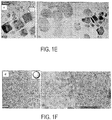
- FIG. 1C is a TEM image of WO 2.72 nanorods that were produced absent any cesium doping, with an inset illustrated rod shape. It has been previously observed in CeO 2 and Re 2 O 3 that changing the ratio of OlAc to OlAm provides shape control as a result of different binding capabilities of the ligands and passivation into the surface of the nanocrystal. Similarly, when cesium was incorporated, increasing the amount of OlAc produces more faceted shapes. As shown in FIGs. 1D-1F , different shapes were achieved depending on the ratio of OlAc to OlAm. Specifically, FIGs.
- 1D-1F are TEM images of Cs x WO 3 hexagonal prisms, cubes and pseudo-spheres, respectively, each with a corresponding inset illustrated shape.
- Hexagonal prisms result when the OlAc:OlAm ratio is 12.5-31, truncated cubes when the ratio is 5.2-12.5, and pseudo-spheres when the ratio is 2.1-5.2.
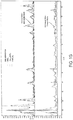
- FIG. 1G illustrates XRD patterns for samples synthesized using 0 mmol OlAc: 10.6 mmol OlAm and 10.6 mmol OlAc:O mmol OlAm with simulated data for Cs 0.29 WO 3 (ICSD: 56223), CsW 2 O 6 [Cs 0.5 WO 3 ] (ICSD: 72634.), and WO 3 (ICSD: 32001), which are not phase pure at these extremes of the surfactant composition.
- an OlAc:OlAm ratio of less than 2.1 or greater than 31.3 results in mixed crystalline phases by XRD.
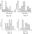
- Particle sizes were determined by TEM to be 16.0 ⁇ 5.8 nm for the undoped WO 2.72 rods (measuring the long dimension), 4.6 ⁇ 0.79 nm for the Cs x WO 3 pseudo-spheres, 20.4+2.4 nm for truncated cubes, and 13.2+3.0 nm for hexagonal prisms.
- the truncated cube particles included a variety of smaller sizes (under 12 nm) besides the primary product that were omitted from size measurements.
- FIG. 1H-1K are size histograms showing data collected from bright field TEM images including 50-100 particles each of undoped WO 2.72 rods, Cs 0.29 WO 3 hexagonal prisms, Cs 0.29 WO 3 truncated cubes, and Cs 0.29 WO 3 pseudo-spheres, respectively.
- FIG. 1L is a scanning electron microscopy (SEM) image of Cs 0.29 WO 3 hexagonal prisms.
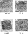
- FIG. 2A is a high resolution lattice-resolved TEM image of undoped WO 2.72 rods with a [-2 4 1] zone axis.
- FIG. 2B is a high resolution lattice-resolved TEM image of a Cs 0.29 WO 3 hexagonal prism viewed perpendicular to its largest face with a [-1 0 1] zone axis.
- FIG. 2C is a high resolution lattice-resolved TEM image of a truncated cube with a [1 0 0] zone axis.
- FIG. 2D is a high resolution lattice-resolved TEM image of pseudo-spheres with a [1 0 0] zone axis.
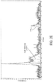
- FIG. 2E is an XRD pattern for WO 2.72 compared to a bulk reference pattern (ICSD: 24731).
- undoped tungsten oxide is consistent with monoclinic WO 2.72 , supporting the assignment of the composition as WO 3-x where x is 0.28.
- the WO 3-x structure is a reduced form of cubic WO 3 that contains oxygen vacancies within the crystal lattice. These oxygen vacancies create a distribution of W formal oxidation states between 6+, 5+, and 4+, and the alterations in charge state are responsible for changes in absorption properties compared to WO 3 . This is apparent by the dark blue color of the nanorods, which results from the tail of the strong infrared spectrum absorption crossing into the red edge of the visible spectrum.
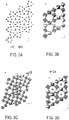
- WO 3 may be described as a modification of the perovskite-type ABO 3 lattice in which the B site is occupied by W atoms and the A site is unoccupied, as shown in FIG. 3A , which is a ball-and-stick model of WO 3 . Oxygen vacancies within the lattice result in the formation of WO 6 octahedron as the basic structural unit.
- FIG. 3B is a polyhedral model of WO 3 , which shows that these oxygen vacancies are responsible for creating tunnels within the crystal structure of WO 2.72 .
- FIG. 3C is a polyhedral model of WO 2.72 showing that additional oxygen vacancies distort the WO 6 octahedral units and the local environments of the tungsten ions become heterogeneous. Doping with Cs + ions instead results in occupation of the open channels in the WO 3 structure to form Cs x WO 3 . This is shown in FIG. 3D , which is a polyhedral model of Cs x WO 3 .
- FIG. 3E shows XRD patterns for Cs 0.29 WO 3 spheres, truncated cubes, and hexagonal prisms.
- the three shapes of cesium tungsten bronze i.e., hexagonal prism, truncated cube, and pseudo-sphere
- XRD patterns were refined by Le Bail fitting in the GSAS suite for the hexagonal prisms (Rp 0.2091; wRp 0.1101) and truncated cubes (Rp 0.1485; wRp 0.0984).
- FIG. 3F is a Le Bail fit with residual plot of a 20.4 ⁇ 2.4 nm truncated cubes.
- FIG. 3G is a Le Bail fit with residual plot of 13.2 ⁇ 3.0 nm hexagonal prisms. The unit cell increases slightly in size when comparing the truncated cube to the hexagonal prism, with respective increases from 7.395 ⁇ to 7.404 ⁇ for the pattern shown in FIGs. 3E and 3F , and 7.606 ⁇ to 7.615 ⁇ for the pattern shown in FIG. 3G .
- FIG. 3H shows a survey scan in FIG. 3H.
- FIGs. 3I and 3J are high resolution scans of Cs 0.29 WO 3 showing normalized peak area measurements for tungsten and cesium respectively.
- FIG. 3K is a table detailing peak fit parameters and composition analysis for Cs 0.29 WO 3 .
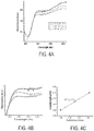
- FIG. 4A illustrates the absorbance spectra of the hexagonal prism Cs 0.29 WO 3 in these solvents, showing two distinct absorbance peaks. While the longer wavelength peak is too broad to draw any definitive conclusions as to the peak shift, there is an obvious red-shift in the shorter wavelength peak as RI changes.
- FIG. 4B is a magnification of the shorter wavelength absorbance peak for the hexagonal prism Cs 0.29 WO 3 in TCE, DMF and MeCN.
- FIG. 4C is a plot showing solvent RI versus wavelength for the hexagonal prism Cs 0.29 WO 3 .
- Re ⁇ 1 ⁇ ⁇ p 2 ⁇ 2 + ⁇ 2
- ⁇ p the plasmon frequency of the bulk metal
- ⁇ represents frequency of incident light
- ⁇ damping frequency of bulk material
- Equation 1 ⁇ p 2 ⁇ med + 1
- FIG. 4D shows SPR peak position of experimental data and the theoretical prediction using Mie's solution to Maxwell's equation plotted against the RI of the surround medium (theory) or solvent (experiment).
- the data show that Mie's solution to Maxwell's equation predicts a stronger dependence of the peak wavelength on RI than was observed experimentally. This difference can be ascribed to the non-spherical shape of the particles as well as the contribution of the ligands attached to the surface of the nanocrystals.
- Noguez discusses SPRs for a series of silver nanoparticle shapes, explaining how the optical peaks change when increasing the number of truncations of a cube (see C. Noguez, J. Phys. Chem C., 2007, 111, 3806-3819 ). That is, truncating a cube results in shapes with different numbers of planes or faces; cube (6 faces), truncated cube (14 faces), icosohedron (20 faces), and sphere (infinite faces). As the number of faces on the particle increases, three important trends are apparent in the resonance spectra. First, the main/largest resonance will blue-shift. Second, the peaks with smaller wavelength resonances move closer to the main resonance and can be hidden. Third, the width of the main resonance peak increases.
- FIG. 5A shows flat projections of a hexagonal prism and truncated cube, with eight and ten faces respectively (a sphere has an infinite number of faces so is not depicted).
- FIG. 5B shows the absorbance spectra of Cs x WO 3 hexagonal prisms (top line), truncated cubes (second from top line), pseudo-spheres (second from bottom line), and WO 2.72 rods (bottom line), with spectra offset for clarity.
- the hexagonal prism has two distinct absorbance peaks, a less intense peak at 860 nm (peak 1) and a more intense peak at 1602 nm (peak 2).
- peak 1 As the number of faces on the nanocrystal surface increases from eight (hexagonal prism) to ten (truncated cube) to infinity (sphere), the optical peaks reduce from two obvious, distinct peaks to one. This is observed as the number of faces increase with a red-shift of peak 1 (respectively 860 nm, 990 nm, 1315 nm) and a blue-shift of peak 2 (respectively 1602 nm, 1506 nm, and 1315 nm). As the trend of increasing the faces of the particles progresses, peak 1 becomes less visible. In effect, peak 1 in the pseudo-sphere sample becomes indistinguishable from peak 2, so that both resonances occur under the envelope of one broader peak.
- FIG. 5B shows the absorbance spectra of WO 2.72 with a broad peak at approximately 2100 nm. This spectrum is sharply contrasted with those that result from doping with cesium, which changes the crystal structure from monoclinic to hexagonal.
- Adachi has suggested that peak 2 in Cs x WO 3 is a shift of the polaron seen in WO 2.72 (see K. Adachi et al., J. Mater. Res. 2012, 27, 965-970 ).
- Doped plasmonic materials have substantially lower carrier densities, such as Cu 1.85 Se with a carrier density of 3.0 x 1021cm -3 and indium tin oxide with a density of 1.9 x 1021 cm -3 .
- the carrier density for the synthesized faceted Cs x WO 3 particles cannot be rigorously derived from their optical spectra without detailed electromagnetic modeling, but it was approximated by Drude theory to be as high as 5 x 1021cm -3 .
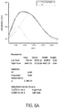
- FIG. 6A illustrates Gaussian peak fit of pseudo sphere absorbance spectra including calculated parameters, statistics, and calculated carrier density.
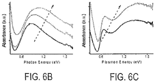
- FIG. 6B shows the absorbance spectra of a Cs x WO 3 pseudo-sphere sample, with aliquots of the same reaction taken at 5 mins (bottom line), 30 mins (middle line), and 60 mins (top line). As the reaction progresses the particle size increases from roughly 3 nm to 5 nm, and there is an obvious red-shift of the resonance peak from 1081 nm at 5 min to 1350 nm at 60 min.
- FIG. 6A illustrates Gaussian peak fit of pseudo sphere absorbance spectra including calculated parameters, statistics, and calculated carrier density.
- FIG. 6B shows the absorbance spectra of a Cs x WO 3 pseudo-sphere sample, with aliquots of the same reaction taken at 5 mins (bottom line), 30 mins (middle line), and 60 mins (top line). As the reaction progresses the particle size increases from
- 6C shows the absorbance spectra of a Cs x WO 3 hexagonal prism sample, with aliquots of the same reaction taken at 30 mins (bottom line) and 90 mins (top line). As the reaction progresses from 30 min to 90 min the plasmon peaks shift from 835 nm to 870 nm and 1840 m to 1962 nm. These shifts in spectra follow the same qualitative trends reported in the literature for 5-40 nm gold rods (with fixed 2.4 aspect ratio), and 9-99 nm gold spheres.
Landscapes
- Physics & Mathematics (AREA)
- Nonlinear Science (AREA)
- Chemical & Material Sciences (AREA)
- Inorganic Chemistry (AREA)
- General Physics & Mathematics (AREA)
- Optics & Photonics (AREA)
- Crystallography & Structural Chemistry (AREA)
- Electrochromic Elements, Electrophoresis, Or Variable Reflection Or Absorption Elements (AREA)
Claims (10)
- Fenêtre électrochrome (100) comprenant :au moins une couche conductrice transparente (102a, 102b) ;une couche de bronze d'oxyde métallique de transition nanostructuré (112) comprenant : un ou plusieurs oxydes de métal de transition comprenant au moins un oxyde parmi l'oxyde de niobium, de tungstène, de molybdène, de vanadium et de titane, et un ou plusieurs dopants ; un électrolyte à l'état solide (106) ; et une contre-électrode (108),dans laquelle le bronze d'oxyde métallique de transition nanostructuré (112) module sélectivement, indépendamment, la transmittance du rayonnement du spectre proche infrarouge (NIR) et du rayonnement du spectre visible en fonction d'une tension appliquée au dispositif,dans laquelle les un ou plusieurs dopants comprennent au moins un dopant parmi :une espèce dopante qui provoque un effet de résonance plasmonique de surface sur les un ou plusieurs oxydes métalliques de transition en créant des porteurs d'électrons délocalisés qui modulent sélectivement la transmittance du rayonnement du spectre NIR en réponse à une première tension appliquée au dispositif, l'espèce dopante comprenant au moins un ion parmi les ions césium, cérium, lanthane, praséodyme, néodyme, prométhium, samarium, europium, gadolinium, terbium, dysprosium, holmium, erbium, thulium, ytterbium, lutétium et rubidium ; etune espèce d'intercalation qui provoque un changement dans l'état d'oxydation des ions métalliques de transition dans l'oxyde métallique de transition en raison de l'intercalation dans l'oxyde métallique et de la désintercalation de ce dernier, qui module sélectivement la transmittance du rayonnement du spectre visible en réponse à une deuxième tension appliquée au dispositif, dans laquelle la deuxième tension appliquée a une valeur absolue plus grande que la première tension appliquée, l'espèce d'intercalation comprenant au moins l'une d'une espèce d'intercalation comprenant au moins l'un des ions lithium, sodium, potassium, rubidium, césium, béryllium, magnésium, calcium, strontium, baryum, des ions cérium, lanthane, praséodyme, néodyme, prométhium, samarium, europium, gadolinium, terbium, dysprosium, holmium, erbium, thulium, ytterbium ou lutétium ; et d'une espèce de proton chargée.
- Fenêtre électrochrome selon la revendication 1, dans laquelle :la couche de bronze d'oxyde métallique de transition nanostructuré (112) comprend une pluralité de nanoparticules ; l'électrolyte à l'état solide (106) est un matériau comprenant au moins un polymère comprenant du polyvinylbutyral (PVB), un sel de lithium comprenant du bis(trifluorométhane) de lithium et 40 à 60 % en poids d'un plastifiant ; etle matériau d'électrolyte à l'état solide pénètre dans des crevasses entre les nanoparticules de la couche de bronze d'oxyde métallique de transition nanostructuré (112).
- Fenêtre électrochrome selon la revendication 1, dans laquelle :l'électrolyte à l'état solide (106) comprend de l'oxynitrure de lithium et de phosphore (LiPON) ou du Ta2O5 ; etla contre-électrode (108) comprend un matériau d'électrode passive choisi parmi le CeO2, le CeVO2, le TiO2, l'oxyde d'indium et d'étain, l'oxyde d'indium, l'oxyde d'étain, l'oxyde d'étain dopé au manganèse ou à l'antimoine, l'oxyde de zinc dopé à l'aluminium, l'oxyde de zinc, l'oxyde de gallium et de zinc, l'oxyde d'indium, de gallium et de zinc, l'oxyde d'indium dopé au molybdène, le Fe2O3 et le V2O5, ou un matériau d'électrode complémentaire choisi parmi le Cr2O3, le MnO2, le FeO2, le CoO2, le NiO2, le RhO2 et l'IrO2.
- Fenêtre électrochrome selon la revendication 3, dans laquelle :au moins l'un des un ou plusieurs oxydes métalliques de transition comprend de l'oxyde de tungstène (WO3-x), où 0 ≤ x ≤ 0,1, ou du Nb:TiO2 ; etdans laquelle au moins l'une des une ou plusieurs espèces dopantes comprend des ions césium.
- Fenêtre électrochrome selon la revendication 1, dans laquelle la couche de bronze d'oxyde métallique de transition nanostructuré (112) comprend des nanoparticules ayant au moins 20 facettes.
- Fenêtre électrochrome selon la revendication 1, dans laquelle :la tension appliquée comprend des première et deuxième tensions comprises entre -5 V et 5 V, ou entre -2 V et 2 V ; etla première tension comprend une polarisation positive configurée de telle sorte que la couche de bronze d'oxyde métallique de transition nanostructuré (112) est transparente au rayonnement du spectre NIR et au rayonnement du spectre visible ;la deuxième tension comprend une polarisation négative configurée de telle sorte que la couche de bronze d'oxyde métallique de transition nanostructuré (112) absorbe le rayonnement du spectre NIR et est transparente au rayonnement du spectre visible ; etl'augmentation de la deuxième tension de polarisation négative appliquée amène la couche de bronze d'oxyde métallique de transition nanostructuré (112) à absorber le rayonnement du spectre visible et le rayonnement du spectre NIR.
- Procédé de fonctionnement d'une fenêtre électrochrome comprenant au moins une couche conductrice transparente, une couche de bronze d'oxyde métallique de transition nanostructuré (112) comprenant :un ou plusieurs oxydes métalliques de transition comprenant au moins un oxyde parmi l'oxyde de niobium, de tungstène, de molybdène, de vanadium et de titane, et un ou plusieurs dopants, un électrolyte à l'état solide (106) et une contre-électrode (108), dans lequel le procédé comprend :l'application d'une première tension au dispositif de telle sorte que le bronze d'oxyde métallique de transition nanostructuré (112) module sélectivement la transmittance du rayonnement du spectre proche infrarouge (NIR) ; etl'application d'une deuxième tension ayant une valeur absolue plus grande que la première tension au dispositif de telle sorte que le bronze d'oxyde métallique de transition nanostructuré (112) module sélectivement la transmittance du rayonnement du spectre visible,dans lequel les un ou plusieurs dopants comprennent au moins une espèce parmi :une espèce dopante qui provoque un effet de résonance plasmonique de surface sur les un ou plusieurs oxydes métalliques de transition en créant des porteurs d'électrons délocalisés qui modulent sélectivement la transmittance du rayonnement du spectre NIR en réponse à la première tension appliquée au dispositif, l'espèce dopante comprenant au moins un ion parmi les ions césium, cérium, lanthane, praséodyme, néodyme, prométhium, samarium, europium, gadolinium, terbium, dysprosium, holmium, erbium, thulium, ytterbium, lutétium et rubidium ; ouune espèce d'intercalation qui provoque un changement dans l'état d'oxydation des ions métalliques de transition dans l'oxyde métallique de transition en raison de l'intercalation dans l'oxyde métallique et de la désintercalation de ce dernier, qui module sélectivement la transmittance du rayonnement du spectre visible en réponse à la deuxième tension appliquée au dispositif, dans laquelle la deuxième tension appliquée a une valeur absolue plus grande que la première tension appliquée, l'espèce d'intercalation comprenant au moins l'une d'une espèce d'intercalation comprenant au moins l'un des ions lithium, sodium, potassium, rubidium, césium, béryllium, magnésium, calcium, strontium, baryum, des ions cérium, lanthane, praséodyme, néodyme, prométhium, samarium, europium, gadolinium, terbium, dysprosium, holmium, erbium, thulium, ytterbium ou lutétium ; et d'une espèce de proton chargée.
- Procédé selon la revendication 7, dans lequel :la couche de bronze d'oxyde métallique de transition nanostructuré (112) comprend une pluralité de nanoparticules d'oxyde de tungstène (WO3-x), où 0 ≤ x ≤ 0,1 ;l'au moins une des une ou plusieurs espèces dopantes comprend des ions césium ;l'électrolyte à l'état solide (106) est un matériau comprenant au moins un polymère, un sel de lithium et un plastifiant ; etle matériau d'électrolyte à l'état solide pénètre dans des crevasses entre les nanoparticules de la couche de bronze d'oxyde métallique de transition nanostructuré (112).
- Procédé selon la revendication 8, dans lequel :les première et deuxième tensions sont comprises entre -5 V et 5 V ;la première tension comprend une polarisation négative qui amène la couche de bronze d'oxyde métallique de transition nanostructuré (112) à absorber le rayonnement du spectre NIR et à rester transparente au rayonnement du spectre visible ;la deuxième tension comprend une polarisation négative ayant une amplitude plus grande que la première tension qui amène la couche de bronze d'oxyde métallique de transition nanostructuré (112) à absorber le rayonnement du spectre visible et le rayonnement du spectre NIR ; etle procédé comprend en outre l'application d'une troisième tension qui comprend une polarisation positive au dispositif pour amener la couche de bronze d'oxyde métallique de transition nanostructuré (112) à devenir transparente au rayonnement du spectre NIR et au rayonnement du spectre visible.
- Utilisation d'un dispositif électrochrome pour améliorer des changements optiques dans des fenêtres, dans laquelle le dispositif comprend :au moins une couche conductrice transparente ;une couche de bronze d'oxyde métallique de transition nanostructurée (112) comprenant : un ou plusieurs oxydes métalliques de transition comprenant au moins un oxyde parmi l'oxyde de niobium, de tungstène, de molybdène, de vanadium et de titane, et un ou plusieurs dopants ; un électrolyte à l'état solide (106) ; et une contre-électrode (108),dans laquelle le bronze d'oxyde métallique de transition nanostructuré (112) module sélectivement, indépendamment, la transmittance du rayonnement du spectre proche infrarouge (NIR) et du rayonnement visible en fonction d'une tension appliquée au dispositif, etdans laquelle les un ou plusieurs dopants comprennent au moins une espèce parmi :une espèce dopante qui provoque un effet de résonance plasmonique de surface sur les un ou plusieurs oxydes métalliques de transition en créant des porteurs d'électrons délocalisés qui modulent sélectivement la transmittance du rayonnement du spectre NIR en réponse à une première tension appliquée au dispositif, l'espèce dopante comprenant au moins un ion parmi les ions césium, cérium, lanthane, praséodyme, néodyme, prométhium, samarium, europium, gadolinium, terbium, dysprosium, holmium, erbium, thulium, ytterbium, lutétium et rubidium ; etune espèce d'intercalation qui provoque un changement dans l'état d'oxydation des ions métalliques de transition dans l'oxyde métallique de transition en raison de l'intercalation dans l'oxyde métallique et de la désintercalation de ce dernier, qui module sélectivement la transmittance du rayonnement du spectre visible en réponse à une deuxième tension appliquée au dispositif, dans laquelle la deuxième tension appliquée a une valeur absolue plus grande que la première tension appliquée, l'espèce d'intercalation comprenant au moins l'une d'une espèce d'intercalation comprenant au moins l'un des ions lithium, sodium, potassium, rubidium, césium, béryllium, magnésium, calcium, strontium, baryum, des ions cérium, lanthane, praséodyme, néodyme, prométhium, samarium, europium, gadolinium, terbium, dysprosium, holmium, erbium, thulium, ytterbium ou lutétium ; et d'une espèce de proton chargée.
Applications Claiming Priority (2)
| Application Number | Priority Date | Filing Date | Title |
|---|---|---|---|
| US201461973331P | 2014-04-01 | 2014-04-01 | |
| PCT/US2015/022980 WO2015153337A1 (fr) | 2014-04-01 | 2015-03-27 | Matériau électrochromique nanostructuré d'oxyde métallique de transition conducteur et dispositifs de commutation optique constitués de ceux-ci |
Publications (3)
| Publication Number | Publication Date |
|---|---|
| EP3126905A1 EP3126905A1 (fr) | 2017-02-08 |
| EP3126905A4 EP3126905A4 (fr) | 2017-08-23 |
| EP3126905B1 true EP3126905B1 (fr) | 2020-09-02 |
Family
ID=54190118
Family Applications (1)
| Application Number | Title | Priority Date | Filing Date |
|---|---|---|---|
| EP15774402.0A Active EP3126905B1 (fr) | 2014-04-01 | 2015-03-27 | Fenêtre électrochrome comprenant un matériau électrochrome nanostructuré d'oxyde métallique de transition, méthode de contrôle d'une telle fenêtre électrochrome et utilisation d'un dispositif électrochrome comprenant un tel matériau électrochrome |
Country Status (3)
| Country | Link |
|---|---|
| US (1) | US9785031B2 (fr) |
| EP (1) | EP3126905B1 (fr) |
| WO (1) | WO2015153337A1 (fr) |
Families Citing this family (25)
| Publication number | Priority date | Publication date | Assignee | Title |
|---|---|---|---|---|
| US10983409B2 (en) | 2015-08-26 | 2021-04-20 | Heliotrope Technologies, Inc. | Electrochromic device containing color-tunable nanostructures |
| US9684219B2 (en) | 2015-08-26 | 2017-06-20 | Heliotrope Technologies | Electrochromic device containing color-tunable nanostructures |
| WO2017106160A1 (fr) * | 2015-12-15 | 2017-06-22 | Board Of Regents, The University Of Texas System | Films conducteurs nanostructurés avec répartition hétérogène de dopant et procédés pour leur fabrication et leur utilisation |
| US10310352B2 (en) | 2016-02-01 | 2019-06-04 | Heliotrope Technologies, Inc. | Electrochromic system containing an insulating protective layer and method for controlling photochromic darkening |
| US10156764B2 (en) | 2016-02-01 | 2018-12-18 | Heliotrope Technologies, Inc. | Electrochromic system and method for controlling photochromic darkening |
| US10203582B2 (en) | 2016-02-01 | 2019-02-12 | Heliotrope Technologies, Inc. | Electrochromic system containing a Bragg reflector and method for controlling photochromic darkening |
| JP6665210B2 (ja) * | 2016-02-15 | 2020-03-13 | シャープ株式会社 | エレクトロクロミックデバイス、およびエレクトロクロミックデバイスを備えるスマートウインドウ |
| JP2019070675A (ja) * | 2016-03-02 | 2019-05-09 | Agc株式会社 | エレクトロクロミック調光素子用の積層基板、およびエレクトロクロミック調光素子の製造方法 |
| US10331003B2 (en) | 2016-09-26 | 2019-06-25 | Heliotrope Technologies, Inc. | Electrochromic privacy window |
| US10900277B1 (en) | 2016-10-24 | 2021-01-26 | Heliotrope Technologies, Inc. | Monolithic electrochromic window manufacturing methods |
| US11409176B2 (en) | 2017-12-26 | 2022-08-09 | Heliotrope Europe S.L. | Gel electrolyte precursor compositions, electrochromic devices including gel electrolytes, and manufacturing methods thereof |
| US11048136B2 (en) * | 2018-01-29 | 2021-06-29 | Massachusetts Institute Of Technology | Reprogrammable electro-chemo-optical devices and methods for using the same |
| WO2019173089A1 (fr) | 2018-03-05 | 2019-09-12 | Heliotrope Technologies, Inc. | Procédés de fabrication de dispositifs électrochromiques contenant un électrolyte à semi-conducteurs |
| CN110228795A (zh) * | 2018-03-06 | 2019-09-13 | 中国科学院苏州纳米技术与纳米仿生研究所 | 一种硒化铜纳米颗粒局域表面等离激元的调控方法 |
| US10775649B2 (en) | 2018-05-17 | 2020-09-15 | Cardinal Cg Company | Elastomeric optical device and related methods |
| US11340479B2 (en) | 2018-05-17 | 2022-05-24 | Cardinal Cg Company | Elastomeric optical device and related operation methods |
| US10955716B2 (en) * | 2018-07-17 | 2021-03-23 | Heliotrope Technologies, Inc. | Electrochromic device including capping layer |
| US20210200051A1 (en) * | 2018-08-23 | 2021-07-01 | Nitto Denko Corporation | Ultrathin electrochromic device for high optical modulation |
| EP3800502A1 (fr) | 2019-10-01 | 2021-04-07 | Acondicionamiento Tarrasense | Dispositif électrochromique thermo-responsif à double bande |
| CN111048565B (zh) * | 2019-12-18 | 2023-07-28 | 京东方科技集团股份有限公司 | 显示盖板及其制备方法、显示装置 |
| WO2021216871A1 (fr) * | 2020-04-22 | 2021-10-28 | The Penn State Research Foundation | Films conducteurs laissant passer les uv, empilement optique et leurs procédés de fabrication |
| CN115220137B (zh) * | 2022-07-07 | 2023-07-18 | 南京大学 | 一种光谱反射率调控装置及其制备方法 |
| CN116589199B (zh) * | 2023-04-19 | 2026-01-27 | 青岛大学 | 一种锌型智能电致变色阴极材料及其制备方法 |
| CN116495782A (zh) * | 2023-05-16 | 2023-07-28 | 河南大学 | 一种高稳定纳米铯钨青铜透明隔热粉体及其制备方法和应用 |
| CN117270275A (zh) * | 2023-09-27 | 2023-12-22 | 东莞伏安光电科技有限公司 | 一种电致变色薄膜及其制备方法和电致变色器件 |
Family Cites Families (13)
| Publication number | Priority date | Publication date | Assignee | Title |
|---|---|---|---|---|
| US4150879A (en) | 1976-11-12 | 1979-04-24 | Texas Instruments Incorporated | Solid dry electrochromic display |
| US4325611A (en) | 1979-12-26 | 1982-04-20 | Stanford University | Electrochromic material and electro-optical display using same |
| GB8422262D0 (en) | 1984-09-04 | 1984-10-10 | Green M | Variable transmission optical device |
| JP2000155344A (ja) * | 1998-11-20 | 2000-06-06 | Murakami Corp | エレクトロクロミック素子 |
| WO2003014254A1 (fr) | 2001-08-07 | 2003-02-20 | Midwest Research Institute | Contre-electrode electrochrome |
| US6965509B2 (en) * | 2002-12-02 | 2005-11-15 | The United States Of America As Represented By The Secretary Of The Navy | Poly (3,4-alkylenedioxythiophene)-based capacitors using ionic liquids as supporting electrolytes |
| EP1801815B1 (fr) * | 2004-08-31 | 2020-01-01 | Sumitomo Metal Mining Co., Ltd. | Dispositif de suppression du rayonnement infrarouge et méthode de production |
| US20070076286A1 (en) | 2005-09-23 | 2007-04-05 | Yungeun Sung | Electrochromic device comprising protective inorganic solid electrolyte film and manufacturing method thereof |
| EP2360220B1 (fr) | 2008-11-13 | 2015-03-18 | Sumitomo Metal Mining Co., Ltd. | Particules bloquant les infrarouges, leur procédé de fabrication, dispersion de particules bloquant les infrarouges les utilisant et base bloquant les infrarouges |
| US9664974B2 (en) | 2009-03-31 | 2017-05-30 | View, Inc. | Fabrication of low defectivity electrochromic devices |
| FR2962818B1 (fr) * | 2010-07-13 | 2013-03-08 | Saint Gobain | Dispositif electrochimique a proprietes de transmission optique et/ou energetique electrocommandables. |
| US8717658B2 (en) | 2011-02-09 | 2014-05-06 | Kinestral Technologies, Inc. | Electrochromic multi-layer devices with spatially coordinated switching |
| CN107300819B (zh) * | 2011-07-21 | 2021-03-12 | Sage电致变色显示有限公司 | 同时掺杂有锂和金属掺杂物的电致变色的镍氧化物 |
-
2015
- 2015-03-27 EP EP15774402.0A patent/EP3126905B1/fr active Active
- 2015-03-27 WO PCT/US2015/022980 patent/WO2015153337A1/fr not_active Ceased
- 2015-03-27 US US14/671,061 patent/US9785031B2/en active Active
Non-Patent Citations (1)
| Title |
|---|
| None * |
Also Published As
| Publication number | Publication date |
|---|---|
| US20150277202A1 (en) | 2015-10-01 |
| WO2015153337A1 (fr) | 2015-10-08 |
| US9785031B2 (en) | 2017-10-10 |
| EP3126905A4 (fr) | 2017-08-23 |
| EP3126905A1 (fr) | 2017-02-08 |
Similar Documents
| Publication | Publication Date | Title |
|---|---|---|
| EP3126905B1 (fr) | Fenêtre électrochrome comprenant un matériau électrochrome nanostructuré d'oxyde métallique de transition, méthode de contrôle d'une telle fenêtre électrochrome et utilisation d'un dispositif électrochrome comprenant un tel matériau électrochrome | |
| US9791760B2 (en) | Electrochromic device containing metal oxide nanoparticles and ultraviolet blocking material | |
| Heo et al. | Enhanced coloration efficiency of electrochromic tungsten oxide nanorods by site selective occupation of sodium ions | |
| Mattox et al. | Influence of shape on the surface plasmon resonance of tungsten bronze nanocrystals | |
| Tong et al. | Multivalent‐ion electrochromic energy saving and storage devices | |
| Balaji et al. | Hexagonal tungsten oxide based electrochromic devices: spectroscopic evidence for the Li ion occupancy of four-coordinated square windows | |
| Amate et al. | Bi-functional electrochromic supercapacitor based on hydrothermal-grown 3D Nb2O5 nanospheres | |
| US10359680B2 (en) | Post-temperable nanocrystal electrochromic devices | |
| Xu et al. | Influence of Sb doping on the structural and optical properties of tin oxide nanocrystals | |
| Kalagi et al. | Transmission attenuation and chromic contrast characterization of RF sputtered WO3 thin films for electrochromic device applications | |
| Park et al. | Solvothermal synthesis of oxygen deficient tungsten oxide nano-particle for dual band electrochromic devices | |
| Santhosh et al. | Effect of ablation rate on the microstructure and electrochromic properties of pulsed-laser-deposited molybdenum oxide thin films | |
| Acuña et al. | Sputtering power effects on the electrochromic properties of NiO films | |
| Shen et al. | Effect of pH on the electrochromic and photoluminescent properties of Eu doped WO3 film | |
| Zhang et al. | Synthesis, characterization and dual-band electrochromic properties of Nb-doped WO3 films | |
| Reddy et al. | Synthesis, characterizations, and electrochromic studies of WO3 coated CeO2 nanorod thin films for smart window applications | |
| Kadam et al. | Fabrication of an electrochromic device by using WO3 thin films synthesized using facile single-step hydrothermal process | |
| Zydlewski et al. | Site-selective ion intercalation controls spectral response in electrochromic hexagonal tungsten oxide nanocrystals | |
| Gillissen et al. | Mixed molybdenum–tungsten oxide as dual‐band, VIS–NIR selective electrochromic material | |
| Amorin et al. | Commitment between roughness and crystallite size in the vanadium oxide thin film opto-electrochemical properties | |
| Hammad | Thin films based on electrochromic materials for energy storage performance and smart windows applications: a review | |
| Kadam | Electrochromic properties of ITO/WO3/LiClO4-PC-PMMA-ACN/NiO/ITO framework | |
| Yakovleva et al. | Internal electrochromism in vanadium pentoxide xerogel films | |
| Saravanakannan et al. | A new insight characterization analysis and two photon absorption behaviour of pure and doped vanadium oxide | |
| Zhou et al. | Hexagonal WO₃ nanogranular thin films with oxygen-vacancy engineering for ultra-stable electrochromic energy storage devices |
Legal Events
| Date | Code | Title | Description |
|---|---|---|---|
| STAA | Information on the status of an ep patent application or granted ep patent |
Free format text: STATUS: THE INTERNATIONAL PUBLICATION HAS BEEN MADE |
|
| PUAI | Public reference made under article 153(3) epc to a published international application that has entered the european phase |
Free format text: ORIGINAL CODE: 0009012 |
|
| STAA | Information on the status of an ep patent application or granted ep patent |
Free format text: STATUS: REQUEST FOR EXAMINATION WAS MADE |
|
| 17P | Request for examination filed |
Effective date: 20161012 |
|
| AK | Designated contracting states |
Kind code of ref document: A1 Designated state(s): AL AT BE BG CH CY CZ DE DK EE ES FI FR GB GR HR HU IE IS IT LI LT LU LV MC MK MT NL NO PL PT RO RS SE SI SK SM TR |
|
| AX | Request for extension of the european patent |
Extension state: BA ME |
|
| DAV | Request for validation of the european patent (deleted) | ||
| DAX | Request for extension of the european patent (deleted) | ||
| RIN1 | Information on inventor provided before grant (corrected) |
Inventor name: MILLIRON, DELIA J. Inventor name: GARCIA, GUILLERMO Inventor name: MATTOX, TRACY M. Inventor name: DE TRIZIO, LUCA Inventor name: DAHLMAN, CLAYTON Inventor name: KOO, BONIL |
|
| A4 | Supplementary search report drawn up and despatched |
Effective date: 20170726 |
|
| RIC1 | Information provided on ipc code assigned before grant |
Ipc: G02F 1/15 20060101AFI20170720BHEP |
|
| STAA | Information on the status of an ep patent application or granted ep patent |
Free format text: STATUS: EXAMINATION IS IN PROGRESS |
|
| 17Q | First examination report despatched |
Effective date: 20190724 |
|
| GRAP | Despatch of communication of intention to grant a patent |
Free format text: ORIGINAL CODE: EPIDOSNIGR1 |
|
| STAA | Information on the status of an ep patent application or granted ep patent |
Free format text: STATUS: GRANT OF PATENT IS INTENDED |
|
| INTG | Intention to grant announced |
Effective date: 20200116 |
|
| RIN1 | Information on inventor provided before grant (corrected) |
Inventor name: DE TRIZIO, LUCA Inventor name: GARCIA, GUILLERMO Inventor name: MATTOX, TRACY M. Inventor name: KOO, BONIL Inventor name: DAHLMAN, CLAYTON Inventor name: MILLIRON, DELIA J. |
|
| GRAS | Grant fee paid |
Free format text: ORIGINAL CODE: EPIDOSNIGR3 |
|
| GRAA | (expected) grant |
Free format text: ORIGINAL CODE: 0009210 |
|
| STAA | Information on the status of an ep patent application or granted ep patent |
Free format text: STATUS: THE PATENT HAS BEEN GRANTED |
|
| AK | Designated contracting states |
Kind code of ref document: B1 Designated state(s): AL AT BE BG CH CY CZ DE DK EE ES FI FR GB GR HR HU IE IS IT LI LT LU LV MC MK MT NL NO PL PT RO RS SE SI SK SM TR |
|
| REG | Reference to a national code |
Ref country code: GB Ref legal event code: FG4D |
|
| REG | Reference to a national code |
Ref country code: AT Ref legal event code: REF Ref document number: 1309525 Country of ref document: AT Kind code of ref document: T Effective date: 20200915 Ref country code: CH Ref legal event code: EP |
|
| REG | Reference to a national code |
Ref country code: DE Ref legal event code: R096 Ref document number: 602015058433 Country of ref document: DE |
|
| REG | Reference to a national code |
Ref country code: IE Ref legal event code: FG4D |
|
| REG | Reference to a national code |
Ref country code: LT Ref legal event code: MG4D |
|
| PG25 | Lapsed in a contracting state [announced via postgrant information from national office to epo] |
Ref country code: LT Free format text: LAPSE BECAUSE OF FAILURE TO SUBMIT A TRANSLATION OF THE DESCRIPTION OR TO PAY THE FEE WITHIN THE PRESCRIBED TIME-LIMIT Effective date: 20200902 Ref country code: SE Free format text: LAPSE BECAUSE OF FAILURE TO SUBMIT A TRANSLATION OF THE DESCRIPTION OR TO PAY THE FEE WITHIN THE PRESCRIBED TIME-LIMIT Effective date: 20200902 Ref country code: FI Free format text: LAPSE BECAUSE OF FAILURE TO SUBMIT A TRANSLATION OF THE DESCRIPTION OR TO PAY THE FEE WITHIN THE PRESCRIBED TIME-LIMIT Effective date: 20200902 Ref country code: BG Free format text: LAPSE BECAUSE OF FAILURE TO SUBMIT A TRANSLATION OF THE DESCRIPTION OR TO PAY THE FEE WITHIN THE PRESCRIBED TIME-LIMIT Effective date: 20201202 Ref country code: HR Free format text: LAPSE BECAUSE OF FAILURE TO SUBMIT A TRANSLATION OF THE DESCRIPTION OR TO PAY THE FEE WITHIN THE PRESCRIBED TIME-LIMIT Effective date: 20200902 Ref country code: NO Free format text: LAPSE BECAUSE OF FAILURE TO SUBMIT A TRANSLATION OF THE DESCRIPTION OR TO PAY THE FEE WITHIN THE PRESCRIBED TIME-LIMIT Effective date: 20201202 Ref country code: GR Free format text: LAPSE BECAUSE OF FAILURE TO SUBMIT A TRANSLATION OF THE DESCRIPTION OR TO PAY THE FEE WITHIN THE PRESCRIBED TIME-LIMIT Effective date: 20201203 |
|
| REG | Reference to a national code |
Ref country code: NL Ref legal event code: MP Effective date: 20200902 |
|
| REG | Reference to a national code |
Ref country code: AT Ref legal event code: MK05 Ref document number: 1309525 Country of ref document: AT Kind code of ref document: T Effective date: 20200902 |
|
| PG25 | Lapsed in a contracting state [announced via postgrant information from national office to epo] |
Ref country code: PL Free format text: LAPSE BECAUSE OF FAILURE TO SUBMIT A TRANSLATION OF THE DESCRIPTION OR TO PAY THE FEE WITHIN THE PRESCRIBED TIME-LIMIT Effective date: 20200902 Ref country code: RS Free format text: LAPSE BECAUSE OF FAILURE TO SUBMIT A TRANSLATION OF THE DESCRIPTION OR TO PAY THE FEE WITHIN THE PRESCRIBED TIME-LIMIT Effective date: 20200902 Ref country code: LV Free format text: LAPSE BECAUSE OF FAILURE TO SUBMIT A TRANSLATION OF THE DESCRIPTION OR TO PAY THE FEE WITHIN THE PRESCRIBED TIME-LIMIT Effective date: 20200902 |
|
| PG25 | Lapsed in a contracting state [announced via postgrant information from national office to epo] |
Ref country code: CZ Free format text: LAPSE BECAUSE OF FAILURE TO SUBMIT A TRANSLATION OF THE DESCRIPTION OR TO PAY THE FEE WITHIN THE PRESCRIBED TIME-LIMIT Effective date: 20200902 Ref country code: PT Free format text: LAPSE BECAUSE OF FAILURE TO SUBMIT A TRANSLATION OF THE DESCRIPTION OR TO PAY THE FEE WITHIN THE PRESCRIBED TIME-LIMIT Effective date: 20210104 Ref country code: SM Free format text: LAPSE BECAUSE OF FAILURE TO SUBMIT A TRANSLATION OF THE DESCRIPTION OR TO PAY THE FEE WITHIN THE PRESCRIBED TIME-LIMIT Effective date: 20200902 Ref country code: RO Free format text: LAPSE BECAUSE OF FAILURE TO SUBMIT A TRANSLATION OF THE DESCRIPTION OR TO PAY THE FEE WITHIN THE PRESCRIBED TIME-LIMIT Effective date: 20200902 Ref country code: EE Free format text: LAPSE BECAUSE OF FAILURE TO SUBMIT A TRANSLATION OF THE DESCRIPTION OR TO PAY THE FEE WITHIN THE PRESCRIBED TIME-LIMIT Effective date: 20200902 Ref country code: NL Free format text: LAPSE BECAUSE OF FAILURE TO SUBMIT A TRANSLATION OF THE DESCRIPTION OR TO PAY THE FEE WITHIN THE PRESCRIBED TIME-LIMIT Effective date: 20200902 |
|
| PG25 | Lapsed in a contracting state [announced via postgrant information from national office to epo] |
Ref country code: ES Free format text: LAPSE BECAUSE OF FAILURE TO SUBMIT A TRANSLATION OF THE DESCRIPTION OR TO PAY THE FEE WITHIN THE PRESCRIBED TIME-LIMIT Effective date: 20200902 Ref country code: AT Free format text: LAPSE BECAUSE OF FAILURE TO SUBMIT A TRANSLATION OF THE DESCRIPTION OR TO PAY THE FEE WITHIN THE PRESCRIBED TIME-LIMIT Effective date: 20200902 Ref country code: AL Free format text: LAPSE BECAUSE OF FAILURE TO SUBMIT A TRANSLATION OF THE DESCRIPTION OR TO PAY THE FEE WITHIN THE PRESCRIBED TIME-LIMIT Effective date: 20200902 Ref country code: IS Free format text: LAPSE BECAUSE OF FAILURE TO SUBMIT A TRANSLATION OF THE DESCRIPTION OR TO PAY THE FEE WITHIN THE PRESCRIBED TIME-LIMIT Effective date: 20210102 |
|
| REG | Reference to a national code |
Ref country code: DE Ref legal event code: R097 Ref document number: 602015058433 Country of ref document: DE |
|
| PG25 | Lapsed in a contracting state [announced via postgrant information from national office to epo] |
Ref country code: SK Free format text: LAPSE BECAUSE OF FAILURE TO SUBMIT A TRANSLATION OF THE DESCRIPTION OR TO PAY THE FEE WITHIN THE PRESCRIBED TIME-LIMIT Effective date: 20200902 |
|
| PLBE | No opposition filed within time limit |
Free format text: ORIGINAL CODE: 0009261 |
|
| STAA | Information on the status of an ep patent application or granted ep patent |
Free format text: STATUS: NO OPPOSITION FILED WITHIN TIME LIMIT |
|
| 26N | No opposition filed |
Effective date: 20210603 |
|
| PG25 | Lapsed in a contracting state [announced via postgrant information from national office to epo] |
Ref country code: SI Free format text: LAPSE BECAUSE OF FAILURE TO SUBMIT A TRANSLATION OF THE DESCRIPTION OR TO PAY THE FEE WITHIN THE PRESCRIBED TIME-LIMIT Effective date: 20200902 Ref country code: DK Free format text: LAPSE BECAUSE OF FAILURE TO SUBMIT A TRANSLATION OF THE DESCRIPTION OR TO PAY THE FEE WITHIN THE PRESCRIBED TIME-LIMIT Effective date: 20200902 |
|
| PG25 | Lapsed in a contracting state [announced via postgrant information from national office to epo] |
Ref country code: IT Free format text: LAPSE BECAUSE OF FAILURE TO SUBMIT A TRANSLATION OF THE DESCRIPTION OR TO PAY THE FEE WITHIN THE PRESCRIBED TIME-LIMIT Effective date: 20200902 Ref country code: MC Free format text: LAPSE BECAUSE OF FAILURE TO SUBMIT A TRANSLATION OF THE DESCRIPTION OR TO PAY THE FEE WITHIN THE PRESCRIBED TIME-LIMIT Effective date: 20200902 |
|
| REG | Reference to a national code |
Ref country code: CH Ref legal event code: PL |
|
| GBPC | Gb: european patent ceased through non-payment of renewal fee |
Effective date: 20210327 |
|
| REG | Reference to a national code |
Ref country code: BE Ref legal event code: MM Effective date: 20210331 |
|
| PG25 | Lapsed in a contracting state [announced via postgrant information from national office to epo] |
Ref country code: CH Free format text: LAPSE BECAUSE OF NON-PAYMENT OF DUE FEES Effective date: 20210331 Ref country code: LU Free format text: LAPSE BECAUSE OF NON-PAYMENT OF DUE FEES Effective date: 20210327 Ref country code: LI Free format text: LAPSE BECAUSE OF NON-PAYMENT OF DUE FEES Effective date: 20210331 Ref country code: GB Free format text: LAPSE BECAUSE OF NON-PAYMENT OF DUE FEES Effective date: 20210327 Ref country code: IE Free format text: LAPSE BECAUSE OF NON-PAYMENT OF DUE FEES Effective date: 20210327 |
|
| PG25 | Lapsed in a contracting state [announced via postgrant information from national office to epo] |
Ref country code: BE Free format text: LAPSE BECAUSE OF NON-PAYMENT OF DUE FEES Effective date: 20210331 |
|
| REG | Reference to a national code |
Ref country code: DE Ref legal event code: R081 Ref document number: 602015058433 Country of ref document: DE Owner name: THE REGENTS OF THE UNIVERSITY OF CALIFORNIA, O, US Free format text: FORMER OWNERS: HELIOTROPE TECHNOLOGIES, INC., BERKELEY, CA, US; THE REGENTS OF THE UNIVERSITY OF CALIFORNIA, OAKLAND, CALIF., US Ref country code: DE Ref legal event code: R081 Ref document number: 602015058433 Country of ref document: DE Owner name: HIVISQ TECHNOLOGIES, S.L., ES Free format text: FORMER OWNERS: HELIOTROPE TECHNOLOGIES, INC., BERKELEY, CA, US; THE REGENTS OF THE UNIVERSITY OF CALIFORNIA, OAKLAND, CALIF., US |
|
| PG25 | Lapsed in a contracting state [announced via postgrant information from national office to epo] |
Ref country code: HU Free format text: LAPSE BECAUSE OF FAILURE TO SUBMIT A TRANSLATION OF THE DESCRIPTION OR TO PAY THE FEE WITHIN THE PRESCRIBED TIME-LIMIT; INVALID AB INITIO Effective date: 20150327 |
|
| PG25 | Lapsed in a contracting state [announced via postgrant information from national office to epo] |
Ref country code: CY Free format text: LAPSE BECAUSE OF FAILURE TO SUBMIT A TRANSLATION OF THE DESCRIPTION OR TO PAY THE FEE WITHIN THE PRESCRIBED TIME-LIMIT Effective date: 20200902 |
|
| PG25 | Lapsed in a contracting state [announced via postgrant information from national office to epo] |
Ref country code: MK Free format text: LAPSE BECAUSE OF FAILURE TO SUBMIT A TRANSLATION OF THE DESCRIPTION OR TO PAY THE FEE WITHIN THE PRESCRIBED TIME-LIMIT Effective date: 20200902 |
|
| PG25 | Lapsed in a contracting state [announced via postgrant information from national office to epo] |
Ref country code: TR Free format text: LAPSE BECAUSE OF FAILURE TO SUBMIT A TRANSLATION OF THE DESCRIPTION OR TO PAY THE FEE WITHIN THE PRESCRIBED TIME-LIMIT Effective date: 20200902 |
|
| PG25 | Lapsed in a contracting state [announced via postgrant information from national office to epo] |
Ref country code: MT Free format text: LAPSE BECAUSE OF FAILURE TO SUBMIT A TRANSLATION OF THE DESCRIPTION OR TO PAY THE FEE WITHIN THE PRESCRIBED TIME-LIMIT Effective date: 20200902 |
|
| PGFP | Annual fee paid to national office [announced via postgrant information from national office to epo] |
Ref country code: DE Payment date: 20260327 Year of fee payment: 12 |
|
| PGFP | Annual fee paid to national office [announced via postgrant information from national office to epo] |
Ref country code: FR Payment date: 20260325 Year of fee payment: 12 |