EP3127158B1 - Membranbasierter sensor und verfahren zur robusten herstellung eines membranbasierten sensors - Google Patents
Membranbasierter sensor und verfahren zur robusten herstellung eines membranbasierten sensors Download PDFInfo
- Publication number
- EP3127158B1 EP3127158B1 EP15772419.6A EP15772419A EP3127158B1 EP 3127158 B1 EP3127158 B1 EP 3127158B1 EP 15772419 A EP15772419 A EP 15772419A EP 3127158 B1 EP3127158 B1 EP 3127158B1
- Authority
- EP
- European Patent Office
- Prior art keywords
- membrane
- layer
- trench
- cavity
- spacer
- Prior art date
- Legal status (The legal status is an assumption and is not a legal conclusion. Google has not performed a legal analysis and makes no representation as to the accuracy of the status listed.)
- Active
Links
Images


Classifications
-
- G—PHYSICS
- G01—MEASURING; TESTING
- G01L—MEASURING FORCE, STRESS, TORQUE, WORK, MECHANICAL POWER, MECHANICAL EFFICIENCY, OR FLUID PRESSURE
- G01L9/00—Measuring steady of quasi-steady pressure of fluid or fluent solid material by electric or magnetic pressure-sensitive elements; Transmitting or indicating the displacement of mechanical pressure-sensitive elements, used to measure the steady or quasi-steady pressure of a fluid or fluent solid material, by electric or magnetic means
- G01L9/0041—Transmitting or indicating the displacement of flexible diaphragms
- G01L9/0042—Constructional details associated with semiconductive diaphragm sensors, e.g. etching, or constructional details of non-semiconductive diaphragms
- G01L9/0047—Diaphragm with non uniform thickness, e.g. with grooves, bosses or continuously varying thickness
-
- B—PERFORMING OPERATIONS; TRANSPORTING
- B81—MICROSTRUCTURAL TECHNOLOGY
- B81B—MICROSTRUCTURAL DEVICES OR SYSTEMS, e.g. MICROMECHANICAL DEVICES
- B81B3/00—Devices comprising flexible or deformable elements, e.g. comprising elastic tongues or membranes
- B81B3/0064—Constitution or structural means for improving or controlling the physical properties of a device
- B81B3/0067—Mechanical properties
- B81B3/0072—For controlling internal stress or strain in moving or flexible elements, e.g. stress compensating layers
-
- G—PHYSICS
- G01—MEASURING; TESTING
- G01L—MEASURING FORCE, STRESS, TORQUE, WORK, MECHANICAL POWER, MECHANICAL EFFICIENCY, OR FLUID PRESSURE
- G01L19/00—Details of, or accessories for, apparatus for measuring steady or quasi-steady pressure of a fluent medium insofar as such details or accessories are not special to particular types of pressure gauges
- G01L19/04—Means for compensating for effects of changes of temperature, i.e. other than electric compensation
-
- G—PHYSICS
- G01—MEASURING; TESTING
- G01L—MEASURING FORCE, STRESS, TORQUE, WORK, MECHANICAL POWER, MECHANICAL EFFICIENCY, OR FLUID PRESSURE
- G01L19/00—Details of, or accessories for, apparatus for measuring steady or quasi-steady pressure of a fluent medium insofar as such details or accessories are not special to particular types of pressure gauges
- G01L19/06—Means for preventing overload or deleterious influence of the measured medium on the measuring device or vice versa
-
- G—PHYSICS
- G01—MEASURING; TESTING
- G01L—MEASURING FORCE, STRESS, TORQUE, WORK, MECHANICAL POWER, MECHANICAL EFFICIENCY, OR FLUID PRESSURE
- G01L9/00—Measuring steady of quasi-steady pressure of fluid or fluent solid material by electric or magnetic pressure-sensitive elements; Transmitting or indicating the displacement of mechanical pressure-sensitive elements, used to measure the steady or quasi-steady pressure of a fluid or fluent solid material, by electric or magnetic means
- G01L9/0041—Transmitting or indicating the displacement of flexible diaphragms
- G01L9/0042—Constructional details associated with semiconductive diaphragm sensors, e.g. etching, or constructional details of non-semiconductive diaphragms
- G01L9/0048—Details about the mounting of the diaphragm to its support or about the diaphragm edges, e.g. notches, round shapes for stress relief
-
- G—PHYSICS
- G01—MEASURING; TESTING
- G01L—MEASURING FORCE, STRESS, TORQUE, WORK, MECHANICAL POWER, MECHANICAL EFFICIENCY, OR FLUID PRESSURE
- G01L9/00—Measuring steady of quasi-steady pressure of fluid or fluent solid material by electric or magnetic pressure-sensitive elements; Transmitting or indicating the displacement of mechanical pressure-sensitive elements, used to measure the steady or quasi-steady pressure of a fluid or fluent solid material, by electric or magnetic means
- G01L9/0041—Transmitting or indicating the displacement of flexible diaphragms
- G01L9/0072—Transmitting or indicating the displacement of flexible diaphragms using variations in capacitance
- G01L9/0073—Transmitting or indicating the displacement of flexible diaphragms using variations in capacitance using a semiconductive diaphragm
-
- H—ELECTRICITY
- H04—ELECTRIC COMMUNICATION TECHNIQUE
- H04R—LOUDSPEAKERS, MICROPHONES, GRAMOPHONE PICK-UPS OR LIKE ACOUSTIC ELECTROMECHANICAL TRANSDUCERS; ELECTRIC HEARING AIDS; PUBLIC ADDRESS SYSTEMS
- H04R19/00—Electrostatic transducers
- H04R19/005—Electrostatic transducers using semiconductor materials
-
- H—ELECTRICITY
- H04—ELECTRIC COMMUNICATION TECHNIQUE
- H04R—LOUDSPEAKERS, MICROPHONES, GRAMOPHONE PICK-UPS OR LIKE ACOUSTIC ELECTROMECHANICAL TRANSDUCERS; ELECTRIC HEARING AIDS; PUBLIC ADDRESS SYSTEMS
- H04R19/00—Electrostatic transducers
- H04R19/04—Microphones
-
- B—PERFORMING OPERATIONS; TRANSPORTING
- B81—MICROSTRUCTURAL TECHNOLOGY
- B81B—MICROSTRUCTURAL DEVICES OR SYSTEMS, e.g. MICROMECHANICAL DEVICES
- B81B2201/00—Specific applications of microelectromechanical systems
- B81B2201/02—Sensors
- B81B2201/0257—Microphones or microspeakers
-
- B—PERFORMING OPERATIONS; TRANSPORTING
- B81—MICROSTRUCTURAL TECHNOLOGY
- B81B—MICROSTRUCTURAL DEVICES OR SYSTEMS, e.g. MICROMECHANICAL DEVICES
- B81B2201/00—Specific applications of microelectromechanical systems
- B81B2201/02—Sensors
- B81B2201/0264—Pressure sensors
-
- B—PERFORMING OPERATIONS; TRANSPORTING
- B81—MICROSTRUCTURAL TECHNOLOGY
- B81C—PROCESSES OR APPARATUS SPECIALLY ADAPTED FOR THE MANUFACTURE OR TREATMENT OF MICROSTRUCTURAL DEVICES OR SYSTEMS
- B81C2201/00—Manufacture or treatment of microstructural devices or systems
- B81C2201/01—Manufacture or treatment of microstructural devices or systems in or on a substrate
- B81C2201/0101—Shaping material; Structuring the bulk substrate or layers on the substrate; Film patterning
- B81C2201/0128—Processes for removing material
- B81C2201/013—Etching
- B81C2201/0135—Controlling etch progression
- B81C2201/014—Controlling etch progression by depositing an etch stop layer, e.g. silicon nitride, silicon oxide, metal
-
- H—ELECTRICITY
- H04—ELECTRIC COMMUNICATION TECHNIQUE
- H04R—LOUDSPEAKERS, MICROPHONES, GRAMOPHONE PICK-UPS OR LIKE ACOUSTIC ELECTROMECHANICAL TRANSDUCERS; ELECTRIC HEARING AIDS; PUBLIC ADDRESS SYSTEMS
- H04R31/00—Apparatus or processes specially adapted for the manufacture of transducers or diaphragms therefor
Definitions
- the present disclosure relates to sensors and, more particularly, to microscale membrane sensors.
- Membrane-based sensors such as pressure sensors, acoustic transducers, or microphones, are typically realized using a backside wafer-trench process to define the membrane of the sensor.
- the position and/or the diameter of the backside trench often varies considerably due to the depth of the etching process needed to define the membrane in the sensor.
- the variation of these positional and geometric trench attributes may cause effects such as footing in instances when a trench stops on an oxide layer during formation of the membrane.
- An over-etch may result in a lateral undercut of the sensor structure and, in turn, form a locally larger hole diameter.
- Such diametric variations along the backside trench may lead to a variation in the effective membrane diameter and result in reduced membrane stiffness.
- FIG. 1 shows a cross section of a prior art membrane-based sensor 100 that is susceptible to the positional and dimensional variations discussed above.
- the sensor 100 is shown as a capacitive pressure sensor.
- the sensor 100 has three semiconductor layers which include a substrate or base layer 102, an intermediate layer 104, and a backplate or cap layer 106.
- the sensor 100 also has at least two dielectric layers which include a first oxide layer 108 located between the base layer 102 and the intermediate layer 104 and a second oxide layer 110 located substantially between the intermediate layer 104 and the cap layer 106.
- the first oxide layer 108 electrically decouples the intermediate layer 104 from the base layer 102
- the second oxide layer 110 electrically decouples the intermediate layer 104 from the cap layer 106.
- the cavity 112 is etched through a plurality of vent holes 114 formed in the cap layer 106 and defines an upper surface 116 of the intermediate layer 104.
- the etching of the cavity 112 also defines lower cap portion 118 of the cap layer 106 which is located generally opposite the upper surface 116.
- the vent holes 114 may be closed (not shown) via a thin film or any other encapsulation process so as to enclose a reference pressure or a reference vacuum for a pressure sensor application.
- a backside trench 120 etched from portions of the base layer 102 and the first oxide layer 108 defines a lower surface 122 of the intermediate layer 104.
- the upper surface 116 and the lower surface 122 collectively define the membrane 124 of the sensor 100.
- the conventional deep etching process used to form the backside trench 120 results in considerable positional and diametric variation from wafer to wafer and within a single wafer. In some cases, the diametric variation can be on the order of five (5) to fifty (50) ⁇ m along the backside trench 120.
- the configuration of the membrane 124 within the prior art sensor 100 allows direct coupling of external stress into the membrane 124.
- the behavior of prior art sensors is largely dependent on external stresses induced by the operating environment of the sensor, such as from temperature change, and/or external stresses induced due to manufacturing process, such as during the packaging of the sensor.
- a membrane-based sensor having a backside trench with limited positional and diametric variation from wafer to wafer or within one wafer.
- a sensor device with a membrane substantially decoupled from external stresses is also desirable.
- a robust fabrication method for defining a sensor membrane within a sensor device in a precision controlled manner is further desirable.
- Document US 6,426,239 A1 describes a semiconductor component having a fixed electrode between two flexible diaphragms.
- a hole 601 is formed in a substrate 101 and reaches a pressure-sensor membrane 106 at a lower side.
- a membrane 303 is placed on an upper side of the pressure-sensor membrane 106 with posts 305.
- the invention concerns a membrane-based sensor according to claims 1 to 7 and a method of manufacturing said sensor according to claims 8 to 14.
- FIG. 2 shows a section view of a sensor device 200 according to one embodiment.
- the sensor device 200 has at least three semiconductor layers which include a substrate layer or base layer 202, an intermediate layer 204, and a backplate layer or cap layer 206.
- the sensor device 200 also has at least two dielectric layers which include a first oxide layer 208 located between the base layer 202 and the intermediate layer 204 and a second oxide layer 210 located partially between the intermediate layer 204 and the cap layer 206.
- the first oxide layer 208 electrically decouples the intermediate layer 204 from the base layer 202.
- the second oxide layer 210 partially decouples the intermediate layer 204 from the cap layer 206.
- the second oxide layer 210 includes a plurality of spacers located between the cap layer 206 and the intermediate layer 204.
- the spacers include at least two inner spacers 232 spaced laterally apart from one another and preferably at least two outer spacers 234.
- a first of the outer spacers 234 is spaced outwardly from the left-most one of the inner spacers 232 as viewed in the figure and a second of the outer spacers 234 is spaced outwardly from the right-most one of inner spacers 232 as viewed in the figure.
- the spacers are preferably realized using a perimeter-like closed configuration such that the spacers form a single ring, but they appear in cross section as two separate spacers.
- the peripheral cavity 238 surrounds the central cavity 212 and is separated from the central cavity 212 by the inner spacers 232.
- the cavities are connected to different pressures.
- both cavities are connected to the same pressure.
- the outer peripheral cavity, after formation, is filled with an insulating oxide, a semi-conducting silicon material, or the like.
- the electrode 242 is located above the central cavity 212 and aligned with the upper central surface 236 of the intermediate layer 204.
- a first of the spacer portions 246 is anchored to the first of the inner spacers 232 and a second of the spacer portions 246 is anchored to the second of the inner spacers 232.
- the spacer portions 246 are each laterally insulated from the electrode 242 and from other portions of the cap layer 206 by the trench portions 214, 215.
- a backside trench 220 exposes a lower surface 222 of the intermediate layer 204.
- the inner membrane 224 and the electrode 242 collectively define a capacitor within the sensor device 200.
- the size of the inner membrane 224 is precisely controlled since the positioning of the inner spacers 232 sets the position and the lateral dimension of the inner membrane 224 within the sensor device 200.
- the inner membrane 224 may vary in size by less than one (1) ⁇ m from wafer to wafer or within a single wafer.
- the lower surface 222 and the upper peripheral surface 240 which is located between the inner spacers 232 and the outer spacers 234, collectively define a buffer membrane/buffer area or outer membrane 248 of the sensor device 200.
- the outer membrane 248 does not provide an electrical function and, instead, provides only mechanical function.
- the outer membrane 248 compensates for any variations in the diameter of the backside trench 220 since the position and the size of inner membrane 224 is no longer affected by the diameter of the backside trench 220.
- the outer membrane 248 also compensates for external stress on the sensor device 200 by deflecting slightly under an external load to absorb the external stress.
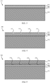
- an oxide layer 310 is formed on a silicon-on-insulator (SOI) wafer 300 which includes a base layer 302, a buried oxide layer 308, and an intermediate layer 304.
- the intermediate layer 304 is a layer of poly- or epitaxial-silicon.
- the oxide layers 308, 310 in the embodiment shown are layers of silicon dioxide (SiO 2 ) that can be, for example, grown by a thermal oxidation process or deposited using PECVD or LPCVD processes.
- FIG. 4 shows the oxide layer 310 patterned to expose portions of the intermediate layer 304. The patterning of the oxide layer 310 forms a central trench portion 314 and a peripheral trench portion 315 spaced outwardly from the central trench portion. In comparing embodiments, only the central trench portion 314 is patterned in the oxide layer 310.
- a layer of silicon is deposited above the patterned oxide layer 310 to form a cap layer 306 of the wafer 300.
- the cap layer 306 is deposited by chemical vapor deposition (CVD) or, more particularly, low pressure chemical vapor deposition (LPCVD), or via epitaxial layer growth.
- the cap layer 306 fills the trench portions 314, 315 and forms a plurality of spacers located between the cap layer 306 and the intermediate layer 304.
- the spacers include at least two inner spacer portions 332 spaced laterally apart from one another and at least two outer spacer portions 334.
- a first of the outer spacer portions 334 is spaced outwardly from the left-most one of the inner spacer portions 332 as viewed in the figure and a second of the outer spacer portions 334 is spaced outwardly from the right-most one of inner spacer portions 332 as viewed in the figure.
- only the inner spacer portions 332 are formed in the wafer 300 during the deposition of the cap layer 306.
- FIG. 6 shows the cap layer 306 of the wafer 300 with a trench portion etched therethrough.
- the trench portion in the embodiment shown includes a central trench portion 350 and a peripheral trench portion 352 spaced outwardly from the central trench portion 350.
- the central trench portion 350 is positioned to expose portions of the oxide layer 310 located between the inner spacers 314, and the peripheral trench portion 352 is positioned to expose portions of the oxide layer 310 located between the inner and the outer spacers 314, 315.
- the etching of the central trench portion 350 electrically isolates an electrode 342 within the cap layer 306.
- the etching of the peripheral trench portion 352 isolates at least two spacer portions 346 within the cap layer 306.
- vents holes (not shown) can also be etched through portions of the cap layer 306 to expose further portions of the oxide layer 310 located between the spacers 314, 315.
- a hydrofluoric acid (HF) vapor etch release is performed which releases entirely the portion of the oxide layer 310 located between the spacers 332, 334.
- the etching process forms a central cavity 312 between the inner spacers 332, the intermediate layer 304, and the cap layer 306.
- the etching process also forms a peripheral cavity 338 between the inner and the outer spacers 332, 334, the intermediate layer 304, and the cap layer 304.
- the central cavity 312 and the central trench portion 350 electrically decouple the electrode 342 from the intermediate layer 304 and the cap layer 306.
- the portion of the intermediate layer 204 exposed by the central cavity 212 defines the inner membrane 224 of the sensor device 200.
- the silicon-filled spacers 232, 234 provide a hard stop during the etching process ( FIG. 6 )
- it is the patterning of the oxide layer 310 ( FIG. 4 ) that defines the position and the size of the central cavity 212 and, therefore, the position and size of the inner membrane 224.
- the formation of the membrane using the above-described process is substantially more controllable than the prior art fabrication methods since the patterning process that defines the membrane is performed through a relatively thin depth (e.g., the oxide layer 210).
- a timed-etch process is no longer relied upon to form the membrane-defining cavity (124 in FIG. 1 ) within the oxide layer since the spacers 232, 234 function as etch stops during formation of the central cavity 212 in the sensor 200.
- the membrane-based sensor produced using the above-described process includes an inner membrane as a sensor membrane and an outer membrane as a buffer membrane.
- the inner membrane is defined by precision-formed anchor structures, and the inner membrane has both electrical and mechanical functionality.
- the outer membrane is also defined by the precision-formed anchor structures, but the outer membrane has only mechanical functionality. In particular, the outer membrane functions to compensate for any process variations and/or non-uniformities during the back-side trench process and for external stress affecting the sensor performance.
- the membrane-based sensor in various embodiments may be a pressure sensor, a capacitive pressure sensor, a microphone, and capacitive microphone.
Landscapes
- Physics & Mathematics (AREA)
- General Physics & Mathematics (AREA)
- Engineering & Computer Science (AREA)
- Chemical & Material Sciences (AREA)
- Analytical Chemistry (AREA)
- Acoustics & Sound (AREA)
- Signal Processing (AREA)
- Mechanical Engineering (AREA)
- Computer Hardware Design (AREA)
- Microelectronics & Electronic Packaging (AREA)
- Pressure Sensors (AREA)
- Measuring Fluid Pressure (AREA)
Claims (14)
- Membranbasierter Sensor, umfassend:ein Substrat (202);eine Membranschicht, die eine Oberseite und eine Unterseite (222) aufweist und die mit der Unterseite auf dem Substrat (202) angeordnet ist;einen Rückseitengraben (220), der auf einer Seite durch die Unterseite definiert wird, wobei sich der Rückseitengraben (220) soweit wie die Unterseite (222) durch das Substrat (202) erstreckt;einen zentralen Hohlraum, der auf einer ersten Seite durch die Oberseite definiert ist und einen peripheren Hohlraum (238), der auf der Oberseite definiert ist;eine Deckschicht (206), die auf der Oberseite angeordnet und über dem zentralen Hohlraum (212) und über dem peripheren Hohlraum (238) positioniert ist, wobei die Deckschicht (206) den zentralen Hohlraum (212) und den peripheren Hohlraum (238) zwischen der Deckschicht (206) und der Oberseite definiert; undeinen ersten Abstandhalter und einen zweiten Abstandhalter, die sich von der Oberseite zur Deckschicht erstrecken und einstückig mit der Deckschicht (206) ausgebildet sind, dadurch gekennzeichnet, dass der erste Abstandhalter mindestens zwei innere Abstandhalter (232) aufweist und der zweite Abstandhalter mindestens zwei äußere Abstandhalter (234) aufweist, wobei die inneren Abstandhalter (232) einen seitlichen Rand des zentralen Hohlraums (206) und eine zweite Seite des zentralen Hohlraums und einen inneren Membranabschnitt der Membranschicht definieren, wobei der periphere Hohlraum (238) den zentralen Hohlraum (212) umgibt und durch die inneren Abstandhalter (232) von dem zentralen Hohlraum (212) getrennt ist, und wobei die äußeren Abstandhalter (232) einen seitlichen Rand des peripheren Hohlraums (206) definieren, wobei der innere Membranabschnitt (224) eine Sensormembran bildet und sich zwischen den ersten Abstandhaltern (232) erstreckt, und wobei die Unterseite (222) und eine periphere Oberseite (240), die zwischen den inneren Abstandhaltern (232) und den äußeren Abstandhaltern (234) angebracht ist, gemeinsam einen äußeren Membranabschnitt als eine Puffermembran (248) definieren.
- Membranbasierter Sensor nach Anspruch 1, wobei ein Bereich der Oberseite, der von dem ersten Abstandhalter umgeben wird, kleiner als ein Bereich der Unterseite ist, der die eine Seite des Rückseitengrabens definiert.
- Membranbasierter Sensor nach Anspruch 1, der außerdem umfasst:
eine Deckelelektrode, die in einem Abschnitt der Deckschicht direkt über dem zentralen Hohlraum definiert ist. - Membranbasierter Sensor nach Anspruch 1, wobei sich der periphere Hohlraum seitlich über den Rückseitengraben hinaus erstreckt.
- Membranbasierter Sensor nach Anspruch 4, der außerdem umfasst:
einen ersten dielektrischen Schichtabschnitt, der zwischen der Deckschicht und der Membranschicht positioniert ist, wobei der erste dielektrische Schichtabschnitt den zweiten Abstandhalter umgibt. - Membranbasierter Sensor nach Anspruch 4, der außerdem umfasst:
einen zweiten dielektrischen Schichtabschnitt, der direkt unter der Membranschicht positioniert ist, wobei der zweite dielektrische Schichtabschnitt den Rückseitengraben umgibt. - Membranbasierter Sensor nach Anspruch 6, wobei der zentrale Hohlraum mit einem Bezugsdruck abgedichtet ist.
- Verfahren zum Bilden eines membranbasierten Sensors, umfassend:Bilden eines zentralen Grabens (314) und eines peripheren Grabenabschnitts (315), der sich in einem Abstand seitlich nach außen von dem zentralen Graben (314) befindet, durch eine erste dielektrische Schicht, um einen ersten Oberseitenabschnitt und einen zweiten Oberseitenabschnitt einer Membranschicht freizulegen, wobei die erste dielektrische Schicht auf der ersten Membranschicht angeordnet ist, und wobei der zentrale Graben und der periphere Graben gebildet werden, indem die erste dielektrische Schicht (310) strukturiert wird;dadurch gekennzeichnet, dass das Verfahren außerdem die folgenden Schritte umfasst:Bilden eines ersten Abstandhalters mit mindestens zwei inneren Abstandhaltern und eines zweiten Abstandhalters mit mindestens zwei äußeren Abstandhaltern, die den ersten Abstandhalter als einen Ätzstopp innerhalb des zentralen Grabens auf dem ersten Oberseitenabschnitt und innerhalb des peripheren Grabens auf dem zweiten Oberseitenabschnitt seitlich umgeben;Bilden einer Deckschicht, die einstückig mit dem ersten Abstandhalter und dem zweiten Abstandhalter ausgebildet wird, indem die Gräben gefüllt werden, wobei die Deckschicht durch eine chemische Gasphasenabscheidung (Chemical Vapor Deposition, CVD) oder eine chemische Niederdruck-Gasphasenabscheidung (Low Pressure Chemical Vapor Deposition, LPCVD) oder ein Epitaxialschichtaufwachsen abgeschieden wird;Ätzen eines zentralen Hohlraums (212) durch die Deckschicht, wobei ein seitlicher Rand des zentralen Hohlraums (212) durch den ersten Abstandhalter als ein Ätzstopp definiert wird;Ätzen eines peripheren Hohlraums durch die Deckschicht, der den zentralen Hohlraum (212) umgibt und der durch die inneren Abstandhalter von dem zentralen Hohlraum (212) getrennt ist, wobei der erste seitliche Rand des peripheren Hohlraums durch den ersten Abstandhalter als ein Ätzstopp definiert wird und wobei ein zweiter seitlicher Rand des peripheren Hohlraums durch den zweiten Abstandhalter als ein Ätzstopp definiert wird, wobei der innere Membranabschnitt (224) eine Sensormembran bildet und sich zwischen den ersten Abstandhaltern (232) erstreckt; undBilden eines Rückseitengrabens (220) in einem Substrat mithilfe eines Ätzens, um eine Unterseite der Membranschicht freizulegen, wobei die Membranschicht auf dem Substrat (202) angeordnet ist, und wobei die Unterseite (222) und eine periphere Oberseite (240), die zwischen den inneren Abstandhaltern (232) und den äußeren Abstandhaltern (234) angebracht ist, gemeinsam einen äußeren Membranabschnitt als eine Puffermembran (248) definieren.
- Verfahren nach Anspruch 8, wobei:das Ätzen des zentralen Hohlraums ein Freilegen eines ersten Bereichs der Oberseite umfasst;das Bilden des Rückseitengrabens ein Freilegen eines zweiten Bereichs der Unterseite umfasst; undwobei der erste Bereich kleiner als der zweite Bereich ist.
- Verfahren nach Anspruch 8, das außerdem umfasst:
Bilden einer Deckelelektrode in einem Abschnitt der Deckschicht, der einwärts von dem zentralen Graben angebracht ist. - Verfahren nach Anspruch 8, wobei das Bilden des Rückseitengrabens umfasst:
Bilden des Rückseitengrabens mit einer seitlichen Ausdehnung, die geringer als eine seitliche Ausdehnung des peripheren Hohlraums ist. - Verfahren nach Anspruch 11, wobei das Bilden der Deckschicht umfasst:
Bilden der Deckschicht mindestens teilweise auf einer Oberseite der ersten dielektrischen Schicht. - Verfahren nach Anspruch 12, wobei das Bilden des Rückseitengrabens umfasst:
Bilden des Rückseitengrabens durch eine zweite dielektrische Schicht, die direkt unter der Membranschicht positioniert wird. - Verfahren nach Anspruch 13, das außerdem umfasst:Einrichten eines gewünschten Drucks in dem zentralen Hohlraum; undAbdichten des zentralen Hohlraums nach dem Einrichten des gewünschten Drucks.
Applications Claiming Priority (2)
| Application Number | Priority Date | Filing Date | Title |
|---|---|---|---|
| US201461975175P | 2014-04-04 | 2014-04-04 | |
| PCT/US2015/024194 WO2015153938A1 (en) | 2014-04-04 | 2015-04-03 | Membrane-based sensor and method for robust manufacture of a membrane-based sensor |
Publications (3)
| Publication Number | Publication Date |
|---|---|
| EP3127158A1 EP3127158A1 (de) | 2017-02-08 |
| EP3127158A4 EP3127158A4 (de) | 2017-11-08 |
| EP3127158B1 true EP3127158B1 (de) | 2019-06-12 |
Family
ID=54241306
Family Applications (1)
| Application Number | Title | Priority Date | Filing Date |
|---|---|---|---|
| EP15772419.6A Active EP3127158B1 (de) | 2014-04-04 | 2015-04-03 | Membranbasierter sensor und verfahren zur robusten herstellung eines membranbasierten sensors |
Country Status (3)
| Country | Link |
|---|---|
| US (1) | US11402288B2 (de) |
| EP (1) | EP3127158B1 (de) |
| WO (1) | WO2015153938A1 (de) |
Cited By (1)
| Publication number | Priority date | Publication date | Assignee | Title |
|---|---|---|---|---|
| US20210031725A1 (en) * | 2019-08-01 | 2021-02-04 | Hyundai Motor Company | Vehicle rain sensor, and wiper system and wiper control method using the same |
Families Citing this family (4)
| Publication number | Priority date | Publication date | Assignee | Title |
|---|---|---|---|---|
| US20160277845A1 (en) * | 2015-03-17 | 2016-09-22 | Dsp Group Ltd. | Mems-based speaker implementation |
| EP3533386A1 (de) * | 2018-02-28 | 2019-09-04 | Koninklijke Philips N.V. | Druckmessung mit kapazitivem drucksensor |
| WO2020108718A1 (en) * | 2018-11-27 | 2020-06-04 | Grundfos Holding A/S | A cover for a pressure sensor |
| CN117836598A (zh) * | 2021-08-31 | 2024-04-05 | 株式会社村田制作所 | 压力传感器元件及压力传感器 |
Family Cites Families (72)
| Publication number | Priority date | Publication date | Assignee | Title |
|---|---|---|---|---|
| US4216401A (en) * | 1978-12-22 | 1980-08-05 | United Technologies Corporation | Surface acoustic wave (SAW) pressure sensor structure |
| JPS60111129A (ja) * | 1983-11-21 | 1985-06-17 | Yokogawa Hokushin Electric Corp | 圧力センサ |
| GB2198611B (en) * | 1986-12-13 | 1990-04-04 | Spectrol Reliance Ltd | Method of forming a sealed diaphragm on a substrate |
| DE4023420A1 (de) * | 1990-07-24 | 1992-01-30 | Pfister Gmbh | Drucksensor |
| JP2517467B2 (ja) * | 1990-10-05 | 1996-07-24 | 山武ハネウエル株式会社 | 静電容量式圧力センサ |
| US5295395A (en) * | 1991-02-07 | 1994-03-22 | Hocker G Benjamin | Diaphragm-based-sensors |
| US5220838A (en) * | 1991-03-28 | 1993-06-22 | The Foxboro Company | Overpressure-protected, differential pressure sensor and method of making the same |
| DE4333099A1 (de) * | 1993-09-29 | 1995-03-30 | Bosch Gmbh Robert | Kraftsensor und Verfahren zur Herstellung eines Kraftsensors |
| US5479827A (en) * | 1994-10-07 | 1996-01-02 | Yamatake-Honeywell Co., Ltd. | Capacitive pressure sensor isolating electrodes from external environment |
| JP3114570B2 (ja) * | 1995-05-26 | 2000-12-04 | オムロン株式会社 | 静電容量型圧力センサ |
| US5891751A (en) * | 1995-06-02 | 1999-04-06 | Kulite Semiconductor Products, Inc . | Hermetically sealed transducers and methods for producing the same |
| US6700174B1 (en) * | 1997-09-25 | 2004-03-02 | Integrated Micromachines, Inc. | Batch fabricated semiconductor thin-film pressure sensor and method of making same |
| US5824910A (en) * | 1997-04-16 | 1998-10-20 | The United States Of America As Represented By The Secretary Of The Navy | Miniature hydrostat fabricated using multiple microelectromechanical processes |
| US6156585A (en) * | 1998-02-02 | 2000-12-05 | Motorola, Inc. | Semiconductor component and method of manufacture |
| US6346742B1 (en) * | 1998-11-12 | 2002-02-12 | Maxim Integrated Products, Inc. | Chip-scale packaged pressure sensor |
| US6604425B1 (en) * | 2000-06-09 | 2003-08-12 | Hrl Laboratories, Llc | Microelectromechanical correlation device and method |
| US6535460B2 (en) * | 2000-08-11 | 2003-03-18 | Knowles Electronics, Llc | Miniature broadband acoustic transducer |
| US6890834B2 (en) * | 2001-06-11 | 2005-05-10 | Matsushita Electric Industrial Co., Ltd. | Electronic device and method for manufacturing the same |
| US6635519B2 (en) * | 2002-01-10 | 2003-10-21 | Agere Systems, Inc. | Structurally supported thin film resonator and method of fabrication |
| US6612178B1 (en) * | 2002-05-13 | 2003-09-02 | Kulite Semiconductor Products, Inc. | Leadless metal media protected pressure sensor |
| JP4090939B2 (ja) * | 2002-05-29 | 2008-05-28 | ニッタ株式会社 | 静電容量式センサおよびその製造方法 |
| JP2004053344A (ja) * | 2002-07-18 | 2004-02-19 | Tem-Tech Kenkyusho:Kk | 荷重変換型の金属ダイヤフラム圧力センサ |
| JP3969228B2 (ja) * | 2002-07-19 | 2007-09-05 | 松下電工株式会社 | 機械的変形量検出センサ及びそれを用いた加速度センサ、圧力センサ |
| US7111518B1 (en) * | 2003-09-19 | 2006-09-26 | Silicon Microstructures, Inc. | Extremely low cost pressure sensor realized using deep reactive ion etching |
| US7247246B2 (en) * | 2003-10-20 | 2007-07-24 | Atmel Corporation | Vertical integration of a MEMS structure with electronics in a hermetically sealed cavity |
| WO2005054804A1 (en) * | 2003-12-04 | 2005-06-16 | National University Of Singapore | Capacitive pressure sensor with a cantilever member |
| US7202560B2 (en) * | 2004-12-15 | 2007-04-10 | Avago Technologies Wireless Ip (Singapore) Pte. Ltd. | Wafer bonding of micro-electro mechanical systems to active circuitry |
| US7442570B2 (en) * | 2005-03-18 | 2008-10-28 | Invensence Inc. | Method of fabrication of a AL/GE bonding in a wafer packaging environment and a product produced therefrom |
| US7622782B2 (en) * | 2005-08-24 | 2009-11-24 | General Electric Company | Pressure sensors and methods of making the same |
| JP4535046B2 (ja) * | 2006-08-22 | 2010-09-01 | ヤマハ株式会社 | 静電容量センサ及びその製造方法 |
| US7651879B2 (en) * | 2005-12-07 | 2010-01-26 | Honeywell International Inc. | Surface acoustic wave pressure sensors |
| JP2007192773A (ja) * | 2006-01-23 | 2007-08-02 | Denso Corp | 圧力センサ素子の取付構造 |
| US7661318B2 (en) * | 2006-02-27 | 2010-02-16 | Auxitrol S.A. | Stress isolated pressure sensing die, sensor assembly inluding said die and methods for manufacturing said die and said assembly |
| GB0605576D0 (en) | 2006-03-20 | 2006-04-26 | Oligon Ltd | MEMS device |
| EP2275793A1 (de) * | 2006-05-23 | 2011-01-19 | Sensirion Holding AG | Drucksensor mit einer Kammer und Herstellungsverfahren dafür |
| US7508040B2 (en) * | 2006-06-05 | 2009-03-24 | Hewlett-Packard Development Company, L.P. | Micro electrical mechanical systems pressure sensor |
| US8081783B2 (en) * | 2006-06-20 | 2011-12-20 | Industrial Technology Research Institute | Miniature acoustic transducer |
| DE102007019638A1 (de) | 2007-04-26 | 2008-10-30 | Robert Bosch Gmbh | Verfahren zur Herstellung eines mikromechanischen Bauelements mit Trenchstruktur zur Rückseitenkontaktierung |
| US7779698B2 (en) * | 2007-11-08 | 2010-08-24 | Rosemount Inc. | Pressure sensor |
| US8096196B2 (en) * | 2007-12-14 | 2012-01-17 | Siemens Ag | Load cell |
| US7891252B2 (en) | 2008-02-01 | 2011-02-22 | Honeywell International Inc. | Method for sensor fabrication and related sensor and system |
| TWI380456B (en) * | 2008-04-30 | 2012-12-21 | Pixart Imaging Inc | Micro-electro-mechanical device and method for making same |
| JP5769964B2 (ja) * | 2008-07-11 | 2015-08-26 | ローム株式会社 | Memsデバイス |
| US7955885B1 (en) * | 2009-01-09 | 2011-06-07 | Integrated Device Technology, Inc. | Methods of forming packaged micro-electromechanical devices |
| JP4973718B2 (ja) * | 2009-01-27 | 2012-07-11 | セイコーエプソン株式会社 | 圧力検出ユニット、及び圧力センサー |
| US7775119B1 (en) * | 2009-03-03 | 2010-08-17 | S3C, Inc. | Media-compatible electrically isolated pressure sensor for high temperature applications |
| US8215176B2 (en) * | 2009-05-27 | 2012-07-10 | Continental Automotive Systems, Inc. | Pressure sensor for harsh media sensing and flexible packaging |
| JP5398411B2 (ja) * | 2009-08-10 | 2014-01-29 | 株式会社東芝 | マイクロ可動デバイスおよびマイクロ可動デバイスの製造方法 |
| US8387464B2 (en) * | 2009-11-30 | 2013-03-05 | Freescale Semiconductor, Inc. | Laterally integrated MEMS sensor device with multi-stimulus sensing |
| JP2013526083A (ja) * | 2010-05-03 | 2013-06-20 | エス3シー インコーポレイテッド | ウエハ上のmemsダイ分離時のチッピングを最小にする方法 |
| JP2012037415A (ja) * | 2010-08-09 | 2012-02-23 | Seiko Epson Corp | 圧力センサー |
| JP2012073163A (ja) * | 2010-09-29 | 2012-04-12 | Seiko Epson Corp | 圧力センサー |
| US8476087B2 (en) * | 2011-04-21 | 2013-07-02 | Freescale Semiconductor, Inc. | Methods for fabricating sensor device package using a sealing structure |
| US8384168B2 (en) * | 2011-04-21 | 2013-02-26 | Freescale Semiconductor, Inc. | Sensor device with sealing structure |
| CN104541141B (zh) | 2012-02-15 | 2017-08-18 | 罗伯特·博世有限公司 | 具有掺杂电极的压力传感器 |
| DE102012203900A1 (de) * | 2012-03-13 | 2013-09-19 | Robert Bosch Gmbh | Bauelement mit einer mikromechanischen Mikrofonstruktur |
| US8984950B2 (en) * | 2012-04-20 | 2015-03-24 | Rosemount Aerospace Inc. | Separation mode capacitors for sensors |
| US9516428B2 (en) * | 2013-03-14 | 2016-12-06 | Infineon Technologies Ag | MEMS acoustic transducer, MEMS microphone, MEMS microspeaker, array of speakers and method for manufacturing an acoustic transducer |
| US9546922B2 (en) * | 2013-08-09 | 2017-01-17 | Continental Automotive Systems, Inc. | Absolute pressure sensor with improved cap bonding boundary |
| US9369808B2 (en) * | 2013-10-17 | 2016-06-14 | Merry Electronics (Shenzhen) Co., Ltd. | Acoustic transducer with high sensitivity |
| US20150109889A1 (en) * | 2013-10-17 | 2015-04-23 | Merry Electronics (Shenzhen) Co., Ltd. | Acoustic transducer with membrane supporting structure |
| EP2871456B1 (de) * | 2013-11-06 | 2018-10-10 | Invensense, Inc. | Drucksensor und Herstellungsmethode für einen Drucksensor |
| DE102014200500A1 (de) * | 2014-01-14 | 2015-07-16 | Robert Bosch Gmbh | Mikromechanische Drucksensorvorrichtung und entsprechendes Herstellungsverfahren |
| TWI550261B (zh) * | 2014-03-17 | 2016-09-21 | 立錡科技股份有限公司 | 微機電壓力計以及其製作方法 |
| DE102014214532B3 (de) * | 2014-07-24 | 2015-10-08 | Robert Bosch Gmbh | Bauteil mit einem MEMS-Bauelement und einer Kappenstruktur mit Medienanschlussöffnung |
| US9340412B2 (en) * | 2014-07-28 | 2016-05-17 | Ams International Ag | Suspended membrane for capacitive pressure sensor |
| CN105874311A (zh) * | 2014-07-29 | 2016-08-17 | 硅微结构股份有限公司 | 具有帽盖限定的隔膜的压力传感器 |
| US9212054B1 (en) * | 2014-10-15 | 2015-12-15 | DunAn Sensing, LLC | Pressure sensors and methods of making the same |
| US9506827B2 (en) * | 2014-10-15 | 2016-11-29 | Dunan Sensing Llc | Pressure sensors and methods of making the same |
| GB2532806A (en) * | 2014-11-25 | 2016-06-01 | Continental Automotive Systems Us Inc | Piezoresistive pressure sensor device |
| TWI583931B (zh) * | 2016-02-02 | 2017-05-21 | Asia Pacific Microsystems Inc | Miniature piezoresistive pressure sensor |
| DE102017200725A1 (de) * | 2017-01-18 | 2018-07-19 | Robert Bosch Gmbh | Mikromechanischer Sensor |
-
2015
- 2015-04-03 EP EP15772419.6A patent/EP3127158B1/de active Active
- 2015-04-03 US US15/301,226 patent/US11402288B2/en active Active
- 2015-04-03 WO PCT/US2015/024194 patent/WO2015153938A1/en not_active Ceased
Non-Patent Citations (1)
| Title |
|---|
| None * |
Cited By (1)
| Publication number | Priority date | Publication date | Assignee | Title |
|---|---|---|---|---|
| US20210031725A1 (en) * | 2019-08-01 | 2021-02-04 | Hyundai Motor Company | Vehicle rain sensor, and wiper system and wiper control method using the same |
Also Published As
| Publication number | Publication date |
|---|---|
| US20170023426A1 (en) | 2017-01-26 |
| WO2015153938A1 (en) | 2015-10-08 |
| US11402288B2 (en) | 2022-08-02 |
| EP3127158A1 (de) | 2017-02-08 |
| EP3127158A4 (de) | 2017-11-08 |
Similar Documents
| Publication | Publication Date | Title |
|---|---|---|
| JP5649474B2 (ja) | 静電容量型圧力センサおよび静電容量型圧力センサの製造方法 | |
| US20200236470A1 (en) | Microelectromechanical electroacoustic transducer with piezoelectric actuation and corresponding manufacturing process | |
| KR101710826B1 (ko) | 반도체 디바이스의 형성 방법 | |
| TWI624954B (zh) | 在單一晶片上的慣性和壓力感測器 | |
| CN102574676B (zh) | 用于制造具有埋腔的mems器件的方法以及由此获得的mems器件 | |
| EP2535310B1 (de) | Mems-bauelemente mit membran und deren herstellungsverfahren | |
| EP2697159B1 (de) | Spacer-definierte elektrode ausserhalb der ebene | |
| EP3127158B1 (de) | Membranbasierter sensor und verfahren zur robusten herstellung eines membranbasierten sensors | |
| EP3052901B1 (de) | Trägheits- und drucksensoren auf einem einzelnen chip | |
| KR20170002947A (ko) | 압력 센서 소자 및 그 제조 방법 | |
| CN106608614B (zh) | Mems结构的制造方法 | |
| TWI652728B (zh) | 用於面外間隔體界定電極的磊晶式多晶矽蝕刻停止 | |
| EP2815219B1 (de) | Drucksensor mit dotierter elektrode | |
| EP3682210B1 (de) | Kapazitive drucksensoren und andere vorrichtungen mit einer aufgehängten membran und mit abgerundeten ecken an einer verankerungskante | |
| US9302906B2 (en) | Capacitive pressure sensor and method | |
| US8430255B2 (en) | Method of accurately spacing Z-axis electrode | |
| KR101197570B1 (ko) | 압저항형 압력센서 및 그의 제조방법 | |
| JP2009139341A (ja) | 圧力センサの製造方法、圧力センサ、半導体装置、電子機器 |
Legal Events
| Date | Code | Title | Description |
|---|---|---|---|
| STAA | Information on the status of an ep patent application or granted ep patent |
Free format text: STATUS: THE INTERNATIONAL PUBLICATION HAS BEEN MADE |
|
| PUAI | Public reference made under article 153(3) epc to a published international application that has entered the european phase |
Free format text: ORIGINAL CODE: 0009012 |
|
| STAA | Information on the status of an ep patent application or granted ep patent |
Free format text: STATUS: REQUEST FOR EXAMINATION WAS MADE |
|
| 17P | Request for examination filed |
Effective date: 20161104 |
|
| AK | Designated contracting states |
Kind code of ref document: A1 Designated state(s): AL AT BE BG CH CY CZ DE DK EE ES FI FR GB GR HR HU IE IS IT LI LT LU LV MC MK MT NL NO PL PT RO RS SE SI SK SM TR |
|
| AX | Request for extension of the european patent |
Extension state: BA ME |
|
| DAV | Request for validation of the european patent (deleted) | ||
| DAX | Request for extension of the european patent (deleted) | ||
| RIN1 | Information on inventor provided before grant (corrected) |
Inventor name: FEYH, ANDO, LARS Inventor name: O'BRIEN, GARY |
|
| A4 | Supplementary search report drawn up and despatched |
Effective date: 20171011 |
|
| RIC1 | Information provided on ipc code assigned before grant |
Ipc: H04R 19/00 20060101ALI20171005BHEP Ipc: G01L 19/04 20060101ALI20171005BHEP Ipc: G01L 9/00 20060101ALI20171005BHEP Ipc: B81C 1/00 20060101ALI20171005BHEP Ipc: G01L 19/06 20060101ALI20171005BHEP Ipc: H01L 27/14 20060101AFI20171005BHEP |
|
| GRAP | Despatch of communication of intention to grant a patent |
Free format text: ORIGINAL CODE: EPIDOSNIGR1 |
|
| STAA | Information on the status of an ep patent application or granted ep patent |
Free format text: STATUS: GRANT OF PATENT IS INTENDED |
|
| RIC1 | Information provided on ipc code assigned before grant |
Ipc: G01L 19/04 20060101ALI20181025BHEP Ipc: G01L 19/06 20060101ALI20181025BHEP Ipc: B81C 1/00 20060101ALI20181025BHEP Ipc: G01L 9/00 20060101ALI20181025BHEP Ipc: H01L 27/14 20060101AFI20181025BHEP Ipc: H04R 19/00 20060101ALI20181025BHEP |
|
| INTG | Intention to grant announced |
Effective date: 20181204 |
|
| GRAS | Grant fee paid |
Free format text: ORIGINAL CODE: EPIDOSNIGR3 |
|
| GRAA | (expected) grant |
Free format text: ORIGINAL CODE: 0009210 |
|
| STAA | Information on the status of an ep patent application or granted ep patent |
Free format text: STATUS: THE PATENT HAS BEEN GRANTED |
|
| AK | Designated contracting states |
Kind code of ref document: B1 Designated state(s): AL AT BE BG CH CY CZ DE DK EE ES FI FR GB GR HR HU IE IS IT LI LT LU LV MC MK MT NL NO PL PT RO RS SE SI SK SM TR |
|
| REG | Reference to a national code |
Ref country code: GB Ref legal event code: FG4D |
|
| REG | Reference to a national code |
Ref country code: CH Ref legal event code: EP |
|
| REG | Reference to a national code |
Ref country code: AT Ref legal event code: REF Ref document number: 1143703 Country of ref document: AT Kind code of ref document: T Effective date: 20190615 |
|
| REG | Reference to a national code |
Ref country code: IE Ref legal event code: FG4D |
|
| REG | Reference to a national code |
Ref country code: DE Ref legal event code: R096 Ref document number: 602015031878 Country of ref document: DE |
|
| REG | Reference to a national code |
Ref country code: NL Ref legal event code: MP Effective date: 20190612 |
|
| REG | Reference to a national code |
Ref country code: LT Ref legal event code: MG4D |
|
| PG25 | Lapsed in a contracting state [announced via postgrant information from national office to epo] |
Ref country code: AL Free format text: LAPSE BECAUSE OF FAILURE TO SUBMIT A TRANSLATION OF THE DESCRIPTION OR TO PAY THE FEE WITHIN THE PRESCRIBED TIME-LIMIT Effective date: 20190612 Ref country code: SE Free format text: LAPSE BECAUSE OF FAILURE TO SUBMIT A TRANSLATION OF THE DESCRIPTION OR TO PAY THE FEE WITHIN THE PRESCRIBED TIME-LIMIT Effective date: 20190612 Ref country code: LT Free format text: LAPSE BECAUSE OF FAILURE TO SUBMIT A TRANSLATION OF THE DESCRIPTION OR TO PAY THE FEE WITHIN THE PRESCRIBED TIME-LIMIT Effective date: 20190612 Ref country code: HR Free format text: LAPSE BECAUSE OF FAILURE TO SUBMIT A TRANSLATION OF THE DESCRIPTION OR TO PAY THE FEE WITHIN THE PRESCRIBED TIME-LIMIT Effective date: 20190612 Ref country code: FI Free format text: LAPSE BECAUSE OF FAILURE TO SUBMIT A TRANSLATION OF THE DESCRIPTION OR TO PAY THE FEE WITHIN THE PRESCRIBED TIME-LIMIT Effective date: 20190612 Ref country code: NO Free format text: LAPSE BECAUSE OF FAILURE TO SUBMIT A TRANSLATION OF THE DESCRIPTION OR TO PAY THE FEE WITHIN THE PRESCRIBED TIME-LIMIT Effective date: 20190912 |
|
| PG25 | Lapsed in a contracting state [announced via postgrant information from national office to epo] |
Ref country code: RS Free format text: LAPSE BECAUSE OF FAILURE TO SUBMIT A TRANSLATION OF THE DESCRIPTION OR TO PAY THE FEE WITHIN THE PRESCRIBED TIME-LIMIT Effective date: 20190612 Ref country code: BG Free format text: LAPSE BECAUSE OF FAILURE TO SUBMIT A TRANSLATION OF THE DESCRIPTION OR TO PAY THE FEE WITHIN THE PRESCRIBED TIME-LIMIT Effective date: 20190912 Ref country code: GR Free format text: LAPSE BECAUSE OF FAILURE TO SUBMIT A TRANSLATION OF THE DESCRIPTION OR TO PAY THE FEE WITHIN THE PRESCRIBED TIME-LIMIT Effective date: 20190913 Ref country code: LV Free format text: LAPSE BECAUSE OF FAILURE TO SUBMIT A TRANSLATION OF THE DESCRIPTION OR TO PAY THE FEE WITHIN THE PRESCRIBED TIME-LIMIT Effective date: 20190612 |
|
| REG | Reference to a national code |
Ref country code: AT Ref legal event code: MK05 Ref document number: 1143703 Country of ref document: AT Kind code of ref document: T Effective date: 20190612 |
|
| PG25 | Lapsed in a contracting state [announced via postgrant information from national office to epo] |
Ref country code: NL Free format text: LAPSE BECAUSE OF FAILURE TO SUBMIT A TRANSLATION OF THE DESCRIPTION OR TO PAY THE FEE WITHIN THE PRESCRIBED TIME-LIMIT Effective date: 20190612 Ref country code: PT Free format text: LAPSE BECAUSE OF FAILURE TO SUBMIT A TRANSLATION OF THE DESCRIPTION OR TO PAY THE FEE WITHIN THE PRESCRIBED TIME-LIMIT Effective date: 20191014 Ref country code: RO Free format text: LAPSE BECAUSE OF FAILURE TO SUBMIT A TRANSLATION OF THE DESCRIPTION OR TO PAY THE FEE WITHIN THE PRESCRIBED TIME-LIMIT Effective date: 20190612 Ref country code: SK Free format text: LAPSE BECAUSE OF FAILURE TO SUBMIT A TRANSLATION OF THE DESCRIPTION OR TO PAY THE FEE WITHIN THE PRESCRIBED TIME-LIMIT Effective date: 20190612 Ref country code: CZ Free format text: LAPSE BECAUSE OF FAILURE TO SUBMIT A TRANSLATION OF THE DESCRIPTION OR TO PAY THE FEE WITHIN THE PRESCRIBED TIME-LIMIT Effective date: 20190612 Ref country code: AT Free format text: LAPSE BECAUSE OF FAILURE TO SUBMIT A TRANSLATION OF THE DESCRIPTION OR TO PAY THE FEE WITHIN THE PRESCRIBED TIME-LIMIT Effective date: 20190612 Ref country code: EE Free format text: LAPSE BECAUSE OF FAILURE TO SUBMIT A TRANSLATION OF THE DESCRIPTION OR TO PAY THE FEE WITHIN THE PRESCRIBED TIME-LIMIT Effective date: 20190612 |
|
| PG25 | Lapsed in a contracting state [announced via postgrant information from national office to epo] |
Ref country code: ES Free format text: LAPSE BECAUSE OF FAILURE TO SUBMIT A TRANSLATION OF THE DESCRIPTION OR TO PAY THE FEE WITHIN THE PRESCRIBED TIME-LIMIT Effective date: 20190612 Ref country code: IT Free format text: LAPSE BECAUSE OF FAILURE TO SUBMIT A TRANSLATION OF THE DESCRIPTION OR TO PAY THE FEE WITHIN THE PRESCRIBED TIME-LIMIT Effective date: 20190612 Ref country code: SM Free format text: LAPSE BECAUSE OF FAILURE TO SUBMIT A TRANSLATION OF THE DESCRIPTION OR TO PAY THE FEE WITHIN THE PRESCRIBED TIME-LIMIT Effective date: 20190612 Ref country code: IS Free format text: LAPSE BECAUSE OF FAILURE TO SUBMIT A TRANSLATION OF THE DESCRIPTION OR TO PAY THE FEE WITHIN THE PRESCRIBED TIME-LIMIT Effective date: 20191012 |
|
| REG | Reference to a national code |
Ref country code: DE Ref legal event code: R097 Ref document number: 602015031878 Country of ref document: DE |
|
| PG25 | Lapsed in a contracting state [announced via postgrant information from national office to epo] |
Ref country code: TR Free format text: LAPSE BECAUSE OF FAILURE TO SUBMIT A TRANSLATION OF THE DESCRIPTION OR TO PAY THE FEE WITHIN THE PRESCRIBED TIME-LIMIT Effective date: 20190612 |
|
| PLBE | No opposition filed within time limit |
Free format text: ORIGINAL CODE: 0009261 |
|
| STAA | Information on the status of an ep patent application or granted ep patent |
Free format text: STATUS: NO OPPOSITION FILED WITHIN TIME LIMIT |
|
| RAP2 | Party data changed (patent owner data changed or rights of a patent transferred) |
Owner name: ROBERT BOSCH GMBH |
|
| PG25 | Lapsed in a contracting state [announced via postgrant information from national office to epo] |
Ref country code: PL Free format text: LAPSE BECAUSE OF FAILURE TO SUBMIT A TRANSLATION OF THE DESCRIPTION OR TO PAY THE FEE WITHIN THE PRESCRIBED TIME-LIMIT Effective date: 20190612 Ref country code: DK Free format text: LAPSE BECAUSE OF FAILURE TO SUBMIT A TRANSLATION OF THE DESCRIPTION OR TO PAY THE FEE WITHIN THE PRESCRIBED TIME-LIMIT Effective date: 20190612 |
|
| 26N | No opposition filed |
Effective date: 20200313 |
|
| PG25 | Lapsed in a contracting state [announced via postgrant information from national office to epo] |
Ref country code: IS Free format text: LAPSE BECAUSE OF FAILURE TO SUBMIT A TRANSLATION OF THE DESCRIPTION OR TO PAY THE FEE WITHIN THE PRESCRIBED TIME-LIMIT Effective date: 20200224 Ref country code: SI Free format text: LAPSE BECAUSE OF FAILURE TO SUBMIT A TRANSLATION OF THE DESCRIPTION OR TO PAY THE FEE WITHIN THE PRESCRIBED TIME-LIMIT Effective date: 20190612 |
|
| PG2D | Information on lapse in contracting state deleted |
Ref country code: IS |
|
| PG25 | Lapsed in a contracting state [announced via postgrant information from national office to epo] |
Ref country code: MC Free format text: LAPSE BECAUSE OF FAILURE TO SUBMIT A TRANSLATION OF THE DESCRIPTION OR TO PAY THE FEE WITHIN THE PRESCRIBED TIME-LIMIT Effective date: 20190612 |
|
| REG | Reference to a national code |
Ref country code: CH Ref legal event code: PL |
|
| PG25 | Lapsed in a contracting state [announced via postgrant information from national office to epo] |
Ref country code: LU Free format text: LAPSE BECAUSE OF NON-PAYMENT OF DUE FEES Effective date: 20200403 Ref country code: LI Free format text: LAPSE BECAUSE OF NON-PAYMENT OF DUE FEES Effective date: 20200430 Ref country code: CH Free format text: LAPSE BECAUSE OF NON-PAYMENT OF DUE FEES Effective date: 20200430 |
|
| REG | Reference to a national code |
Ref country code: BE Ref legal event code: MM Effective date: 20200430 |
|
| PG25 | Lapsed in a contracting state [announced via postgrant information from national office to epo] |
Ref country code: BE Free format text: LAPSE BECAUSE OF NON-PAYMENT OF DUE FEES Effective date: 20200430 |
|
| PG25 | Lapsed in a contracting state [announced via postgrant information from national office to epo] |
Ref country code: IE Free format text: LAPSE BECAUSE OF NON-PAYMENT OF DUE FEES Effective date: 20200403 |
|
| PG25 | Lapsed in a contracting state [announced via postgrant information from national office to epo] |
Ref country code: MT Free format text: LAPSE BECAUSE OF FAILURE TO SUBMIT A TRANSLATION OF THE DESCRIPTION OR TO PAY THE FEE WITHIN THE PRESCRIBED TIME-LIMIT Effective date: 20190612 Ref country code: CY Free format text: LAPSE BECAUSE OF FAILURE TO SUBMIT A TRANSLATION OF THE DESCRIPTION OR TO PAY THE FEE WITHIN THE PRESCRIBED TIME-LIMIT Effective date: 20190612 |
|
| PG25 | Lapsed in a contracting state [announced via postgrant information from national office to epo] |
Ref country code: MK Free format text: LAPSE BECAUSE OF FAILURE TO SUBMIT A TRANSLATION OF THE DESCRIPTION OR TO PAY THE FEE WITHIN THE PRESCRIBED TIME-LIMIT Effective date: 20190612 |
|
| PGFP | Annual fee paid to national office [announced via postgrant information from national office to epo] |
Ref country code: FR Payment date: 20230417 Year of fee payment: 9 Ref country code: DE Payment date: 20230627 Year of fee payment: 9 |
|
| PGFP | Annual fee paid to national office [announced via postgrant information from national office to epo] |
Ref country code: GB Payment date: 20230420 Year of fee payment: 9 |
|
| REG | Reference to a national code |
Ref country code: DE Ref legal event code: R119 Ref document number: 602015031878 Country of ref document: DE |
|
| REG | Reference to a national code |
Ref country code: DE Ref legal event code: R079 Ref document number: 602015031878 Country of ref document: DE Free format text: PREVIOUS MAIN CLASS: H01L0027140000 Ipc: H10F0019500000 |
|
| GBPC | Gb: european patent ceased through non-payment of renewal fee |
Effective date: 20240403 |
|
| PG25 | Lapsed in a contracting state [announced via postgrant information from national office to epo] |
Ref country code: DE Free format text: LAPSE BECAUSE OF NON-PAYMENT OF DUE FEES Effective date: 20241105 |
|
| PG25 | Lapsed in a contracting state [announced via postgrant information from national office to epo] |
Ref country code: GB Free format text: LAPSE BECAUSE OF NON-PAYMENT OF DUE FEES Effective date: 20240403 |
|
| PG25 | Lapsed in a contracting state [announced via postgrant information from national office to epo] |
Ref country code: FR Free format text: LAPSE BECAUSE OF NON-PAYMENT OF DUE FEES Effective date: 20240430 |
|
| PG25 | Lapsed in a contracting state [announced via postgrant information from national office to epo] |
Ref country code: GB Free format text: LAPSE BECAUSE OF NON-PAYMENT OF DUE FEES Effective date: 20240403 Ref country code: FR Free format text: LAPSE BECAUSE OF NON-PAYMENT OF DUE FEES Effective date: 20240430 Ref country code: DE Free format text: LAPSE BECAUSE OF NON-PAYMENT OF DUE FEES Effective date: 20241105 |