EP3127406B1 - Elektrogerät und verfahren zur herstellung eines elektrogerätes - Google Patents
Elektrogerät und verfahren zur herstellung eines elektrogerätes Download PDFInfo
- Publication number
- EP3127406B1 EP3127406B1 EP15709414.5A EP15709414A EP3127406B1 EP 3127406 B1 EP3127406 B1 EP 3127406B1 EP 15709414 A EP15709414 A EP 15709414A EP 3127406 B1 EP3127406 B1 EP 3127406B1
- Authority
- EP
- European Patent Office
- Prior art keywords
- circuit board
- printed circuit
- electrical device
- terminal
- screw
- Prior art date
- Legal status (The legal status is an assumption and is not a legal conclusion. Google has not performed a legal analysis and makes no representation as to the accuracy of the status listed.)
- Active
Links
Images


Classifications
-
- H—ELECTRICITY
- H05—ELECTRIC TECHNIQUES NOT OTHERWISE PROVIDED FOR
- H05K—PRINTED CIRCUITS; CASINGS OR CONSTRUCTIONAL DETAILS OF ELECTRIC APPARATUS; MANUFACTURE OF ASSEMBLAGES OF ELECTRICAL COMPONENTS
- H05K7/00—Constructional details common to different types of electric apparatus
- H05K7/14—Mounting supporting structure in casing or on frame or rack
- H05K7/1422—Printed circuit boards receptacles, e.g. stacked structures, electronic circuit modules or box like frames
- H05K7/1427—Housings
- H05K7/1432—Housings specially adapted for power drive units or power converters
- H05K7/14322—Housings specially adapted for power drive units or power converters wherein the control and power circuits of a power converter are arranged within the same casing
-
- H—ELECTRICITY
- H05—ELECTRIC TECHNIQUES NOT OTHERWISE PROVIDED FOR
- H05K—PRINTED CIRCUITS; CASINGS OR CONSTRUCTIONAL DETAILS OF ELECTRIC APPARATUS; MANUFACTURE OF ASSEMBLAGES OF ELECTRICAL COMPONENTS
- H05K1/00—Printed circuits
- H05K1/18—Printed circuits structurally associated with non-printed electric components
- H05K1/182—Printed circuits structurally associated with non-printed electric components associated with components mounted in printed circuit boards [PCB], e.g. insert-mounted components [IMC]
-
- H—ELECTRICITY
- H05—ELECTRIC TECHNIQUES NOT OTHERWISE PROVIDED FOR
- H05K—PRINTED CIRCUITS; CASINGS OR CONSTRUCTIONAL DETAILS OF ELECTRIC APPARATUS; MANUFACTURE OF ASSEMBLAGES OF ELECTRICAL COMPONENTS
- H05K5/00—Casings, cabinets or drawers for electric apparatus
- H05K5/0026—Casings, cabinets or drawers for electric apparatus provided with connectors and printed circuit boards [PCB], e.g. automotive electronic control units
- H05K5/0069—Casings, cabinets or drawers for electric apparatus provided with connectors and printed circuit boards [PCB], e.g. automotive electronic control units having connector relating features for connecting the connector pins with the PCB or for mounting the connector body with the housing
-
- H—ELECTRICITY
- H05—ELECTRIC TECHNIQUES NOT OTHERWISE PROVIDED FOR
- H05K—PRINTED CIRCUITS; CASINGS OR CONSTRUCTIONAL DETAILS OF ELECTRIC APPARATUS; MANUFACTURE OF ASSEMBLAGES OF ELECTRICAL COMPONENTS
- H05K7/00—Constructional details common to different types of electric apparatus
- H05K7/14—Mounting supporting structure in casing or on frame or rack
- H05K7/1417—Mounting supporting structure in casing or on frame or rack having securing means for mounting boards, plates or wiring boards
- H05K7/142—Spacers not being card guides
-
- H—ELECTRICITY
- H02—GENERATION; CONVERSION OR DISTRIBUTION OF ELECTRIC POWER
- H02K—DYNAMO-ELECTRIC MACHINES
- H02K11/00—Structural association of dynamo-electric machines with electric components or with devices for shielding, monitoring or protection
- H02K11/30—Structural association with control circuits or drive circuits
- H02K11/33—Drive circuits, e.g. power electronics
-
- H—ELECTRICITY
- H02—GENERATION; CONVERSION OR DISTRIBUTION OF ELECTRIC POWER
- H02M—APPARATUS FOR CONVERSION BETWEEN AC AND AC, BETWEEN AC AND DC, OR BETWEEN DC AND DC, AND FOR USE WITH MAINS OR SIMILAR POWER SUPPLY SYSTEMS; CONVERSION OF DC OR AC INPUT POWER INTO SURGE OUTPUT POWER; CONTROL OR REGULATION THEREOF
- H02M7/00—Conversion of AC power input into DC power output; Conversion of DC power input into AC power output
- H02M7/003—Constructional details, e.g. physical layout, assembly, wiring or busbar connections
-
- H—ELECTRICITY
- H02—GENERATION; CONVERSION OR DISTRIBUTION OF ELECTRIC POWER
- H02P—CONTROL OR REGULATION OF ELECTRIC MOTORS, ELECTRIC GENERATORS OR DYNAMO-ELECTRIC CONVERTERS; CONTROLLING TRANSFORMERS, REACTORS OR CHOKE COILS
- H02P27/00—Arrangements or methods for the control of AC motors characterised by the kind of supply voltage
- H02P27/04—Arrangements or methods for the control of AC motors characterised by the kind of supply voltage using variable-frequency supply voltage, e.g. inverter or converter supply voltage
- H02P27/06—Arrangements or methods for the control of AC motors characterised by the kind of supply voltage using variable-frequency supply voltage, e.g. inverter or converter supply voltage using DC to AC converters or inverters
-
- H—ELECTRICITY
- H05—ELECTRIC TECHNIQUES NOT OTHERWISE PROVIDED FOR
- H05K—PRINTED CIRCUITS; CASINGS OR CONSTRUCTIONAL DETAILS OF ELECTRIC APPARATUS; MANUFACTURE OF ASSEMBLAGES OF ELECTRICAL COMPONENTS
- H05K2201/00—Indexing scheme relating to printed circuits covered by H05K1/00
- H05K2201/10—Details of components or other objects attached to or integrated in a printed circuit board
- H05K2201/10007—Types of components
- H05K2201/10015—Non-printed capacitor
Definitions
- the invention relates to an electrical device and a method for producing an electrical device.
- the DE 10 2007 012 818 A1 Fig. 10 shows a semiconductor device with terminals.
- the US 2009/0251843 A1 Fig. 13 shows a vehicle-mounted electrical device and a vehicle in which the electrical device is mounted.
- Fig. 13 is an arrangement for effecting basic interference suppression of a matrix converter.
- the invention is therefore based on the object of developing an electrical device and a method for producing an electrical device, the aim being to improve safety.
- the object is achieved in the electrical device according to the features specified in claim 1 and in the method for producing an electrical device according to the features specified in claim 13.
- connection part has a spacing section and a connecting section, wherein the circuit board is spaced apart from the housing part by means of the spacing section, wherein the connecting portion has a threaded portion, in particular wherein the connecting section is connected in an electrically conductive manner to at least one conductor track on the circuit board.
- connection part can be securely connected to the circuit board.
- connection part can be fitted with further components on the circuit board in one work step and can be soldered to the circuit board with the further components in a further work step.
- environmental protection is improved.
- the printed circuit board and the electrical components fitted on the printed circuit board can advantageously be spaced apart from the housing part by means of the spacing section. So the Dielectric strength of the electrical device improved. Voltage flashovers from the electrical components to the housing part can be avoided.
- connection part is designed as a composite part, the connection section being made of an electrically conductive material, in particular made of metal, the spacing section being made of an electrically insulating material, in particular made of plastic.
- the connecting part can be soldered to the printed circuit board in a simple manner by means of the connecting section.
- the printed circuit board and electrical components fitted on the printed circuit board can be spaced apart from the housing part by means of the spacing section, which is designed to be electrically insulating.
- an air gap between the circuit board with the electrical components and the housing part can be specified. The safety of the electrical appliance is improved.
- the spacer section is designed as a plastic injection-molded part.
- the advantage here is that the spacing section can be produced inexpensively in a simple manner.
- the spacer section is molded onto the connecting section.
- the advantage here is that the spacing section can be securely connected to the connecting section in a simple manner.
- the spacing section can advantageously be produced and connected to the connecting section in a single work step.
- the connecting section is at least partially covered by the spacing section. It is advantageous that the spacing section at least partially surrounds the connecting section. As a result, the connection of the spacing section to the connecting section can be implemented in a mechanically stable and secure manner.
- the spacing section engages around an edge, in particular a sheet metal edge, of the connecting section. It is advantageous here that the spacing section at least partially surrounds the edge of the connecting section. The mechanical stability and the security of the connection of the spacing section to the connecting section are thus improved.
- the circuit board is equipped with electrical components, the spacing section being arranged between the circuit board and the housing part in such a way that the electrical components on the circuit board have a minimum distance from the housing part.
- the advantage here is that the dielectric strength of the electrical device is improved. Thus, the safety of the electrical appliance is improved.
- the distance between the electrical components and the housing part is greater than 5 mm.
- the advantage here is that the breakdown voltage of the electrical device is greater than 10 kV. This enables safe operation of the electrical device even at high operating voltages.
- the connecting section has at least one connecting section, in particular a connecting foot, at least one support section and the threaded section.
- the advantage here is that the connecting section can be made compact.
- the connecting section is made in one piece.
- the advantage here is that the connecting section can be manufactured inexpensively. Components can be saved, so environmental protection is improved.
- the connecting section is designed as a stamped and bent part, in particular as a stamped and bent sheet metal part.
- the advantage here is that the connecting section can be manufactured in a simple manner.
- connection section protrudes through a bore in the circuit board and is soldered to a conductor track of the circuit board.
- connection part can be soldered to the circuit board in the same work step as the electrical components fitted on the circuit board.
- the vertical projection of the support section in the circuit board plane surrounds the vertical projection of the bore in the circuit board plane at an angle in the circumferential direction of the projection of the bore of more than 180 °, in particular more than 230 °.
- the advantage here is that the connection part can be arranged on the printed circuit board so that it does not tip over. The safety when soldering the connection section is improved, since the connection section or the connection sections are securely arranged in the bore or the bores. The risk of a soldering defect can be reduced.
- the support section extends perpendicular to a normal vector of the circuit board plane of the circuit board.
- the advantage here is that the connection part can be arranged on the printed circuit board so that it does not tip over.
- the connection part has a large surface facing the circuit board.
- the surface of the support section facing the printed circuit board is advantageously at least 30% of the total surface of the support section, in particular 40%.
- connection part soldered to the circuit board can be prevented from breaking out.
- the housing part has recesses punched through the housing part, a screw part can be passed through one of the recesses and / or the threaded section is arranged in alignment with the recess, the housing part and the connecting section being connectable in an electrically conductive manner by means of the screw part.
- electrical components on the circuit board can be connected to the earth potential by means of the screw part. This enables an optional connection to the earth potential.
- the electrical device can advantageously be adapted to various applications that require different low-voltage networks for electrical power supply.
- an IT system that is designed as a floating network
- the electrical device is used without a screw part, since the electrical components on the circuit board must be isolated from the earthed housing part.
- IT systems are used in small networks with small dimensions and high demands on fail-safe security, for example in hospitals. Additional protective measures are required for personal protection, such as insulation monitoring devices, Overcurrent protection devices, residual current protection devices and / or fault voltage protection devices.
- low-voltage networks with a neutral conductor such as TN systems or TT systems
- the electrical components are partially connected to the earth potential. This makes it easier to detect residual currents than in an IT system, for example using residual current circuit breakers.
- the low-voltage networks with neutral conductors can therefore be designed much larger than the IT system.
- the recess for the screw part can advantageously be produced in one work step with the further recesses, for example ventilation holes.
- the electrical components can advantageously be connected to the grounded housing part by means of the screw part.
- the electrical device can therefore be used for networks with a neutral conductor as well as for networks without a neutral conductor.
- the adaptation to the respective network takes place in a simple manner by screwing the screw part into the connection part or loosening and removing the screw part.
- the housing part functions as a ground connection.
- the advantage here is that the electrical device can be made compact. Components can be saved. Environmental protection is improved.
- a screw part is passed through a recess in the housing part and screw-connected to the threaded section, in particular this screw connection being designed to be self-locking, the screw part connecting the housing part and the connecting section in an electrically conductive manner.
- a perforated disk is arranged between a screw head of the screw part and the housing part.
- the spacer section has a recess through which the screw part can be passed, in particular passed through.
- the advantage here is that the spacer section can be clamped between the housing part and the connecting section. The contact pressure of the screw part can be evenly distributed over the spacing section that partially surrounds the screw part.
- the elastically designed spacer section advantageously functions as a mechanical damping means against vibrations of the housing part.
- the vibrations of the housing part are dampened and the circuit board is arranged in the housing in a vibration-damped manner.
- the recess extends through the spacing section.
- the spacer section is essentially U-shaped, with a region of the screw part being able to be arranged, in particular arranged, between the legs of the U.
- first capacitors are fitted on the printed circuit board, the first capacitors having a common star point, the star point being connected in an electrically conductive manner to the connecting section of the connection part, in particular by means of conductor tracks.
- the star point is grounded by means of the connection part.
- the advantage here is that the grounding can be carried out in a simple and stable manner.
- first capacitors are fitted on the printed circuit board, the first capacitances having a common star point, the star point being electrical is conductively connected to a fourth capacitance, the fourth capacitance being connected to the connecting section of the connection part, in particular by means of at least one conductor track of the circuit board, the fourth capacitance being arranged electrically between the star point and the connection part, in particular the star point being the fourth capacitance and the connector form a series circuit.
- the fourth capacitance functions as an additional filter, by means of which high-frequency interference currents can be diverted. The tension stability is improved. Thus, the safety of the electrical appliance is improved.
- the fourth capacitance is grounded by means of the connection part.
- second capacitances are fitted on the printed circuit board, the second capacitances forming a series circuit which has a center tap, in particular the center tap being electrically conductively connected to the star point.
- the second capacitances are connected in parallel to a third capacitance, in particular an intermediate circuit capacitor of the converter.
- a third capacitance in particular an intermediate circuit capacitor of the converter.
- the electrical device has a polyphase AC voltage connection on the input side, which has a connection means for each phase, the AC voltage connection feeding a rectifier, with a respective connection means being connected to a respective input pole of the rectifier by means of a respective phase line, each phase line in each case having a tap, a first capacitance being electrically arranged between each tap and the star point.
- the advantage here is that the first capacities act as a filter system for the electrical device. By means of the first capacitances, high-frequency fault currents can be derived to the star point. Thus, the security is improved.
- the electrical device has an inverter, a voltage intermediate circuit with the third capacitance as an intermediate circuit capacitor being arranged between the rectifier and the inverter, in particular wherein the inverter is fed from the third capacitance.
- the electrical device can be implemented as a converter. An electric motor can be fed by means of the converter, the rotational frequency of which can be set by means of the converter.
- a respective first inductance is arranged in each phase line between the respective connection means and the respective tap for the respective first capacitance.
- a respective second inductance is arranged in each phase line between the respective tap for the respective first capacitance and the respective input pole of the rectifier.
- an electrical device series which has at least two variants of electrical devices are that optionally a first or a second variant is produced, wherein in a first method step a circuit board is equipped with at least one connection part and capacitors, wherein the capacitors have a common star point, in particular to which the connection part is connected in an electrically conductive manner, wherein in a second process step the circuit board is arranged in a grounded housing with a housing part, wherein the star point is electrically isolated from the earthed housing during the production of the first variant, wherein, in an optional third method step for producing the second variant, the star point is electrically conductively connected to the grounded housing by passing a connecting means, in particular a screw part, through a recess in the housing part and releasably connecting it to the connection part.
- a connecting means in particular a screw part
- the advantage here is that the electrical device can be easily adapted to operate in ungrounded low-voltage networks or in low-voltage networks with a neutral conductor.
- connection of electrical components to the grounded housing part can advantageously be carried out in a detachable manner.
- the electrical device can therefore be retrofitted for operation in other types of low-voltage networks.
- the screw part is screwed into the connection part in the third method step.
- the advantage here is that the screw part can be connected to and released from the connecting part in a simple manner.
- the screw connection can advantageously be designed to be self-locking.
- the screw part can thus be connected to the connecting part in a vibration-proof manner.
- the screw part is electrically conductively connected to the grounded housing part, in particular wherein the screw part touches the housing part.
- the advantage here is that the screw part functions as an electrical connection means.
- the screw part advantageously has a lower electrical resistance than Cable connections. This enables a low-resistance connection between the grounded housing part and the connection part. So security is improved.
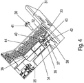
- FIG 4 is a detailed view of the electrical device according to the invention in the second variant drawn in an oblique view, wherein a screw part is shown exploded.
- FIG. 1 The schematic diagram shown shows the electrical device, preferably a converter, with a three-phase AC voltage connection 1, a rectifier 5 and an inverter 8.
- the AC voltage connection 1 has three connection means.
- An inductance (2, 3, 4) is arranged in series with each connection means.
- the rectifier 5 has input poles assigned to the respective phases of the alternating current.
- each phase has a phase line.
- each phase has a branch which is connected to a first capacitance (14, 19, 20).
- the capacitors (14, 19, 20) are connected to a common star point 18.
- the star point 18 can be connected to an earth connection by means of an intermediate connecting means 16.
- a fourth capacitor 15 is arranged between the connecting means 16 and the star point 18.
- a series connection of second capacitances (6, 13) is arranged connected in parallel with a third capacitance 11.
- the second capacitances (6, 13) and the third capacitance 11 are therefore arranged in the DC voltage intermediate circuit.
- the third capacitance 11 is also referred to as an intermediate circuit capacitor.
- the components of the converter are arranged in a housing 10.
- the housing 10 is designed to be at least partially electrically conductive; the housing 10 is preferably made of a metallic material.
- the housing 10 is electrically conductively connected to a ground connection 12 and is therefore grounded.
- the inverter 8 is connected on the output side to a consumer, preferably the consumer is a motor M.
- the consumer has a housing that is electrically connected to a ground connection 9, so the housing of the consumer is grounded.
- FIG. 2 and 4th a detailed view of the second variant of the converter is shown.
- a printed circuit board 38 of the converter is equipped with capacitors (34, 35, 36) which act as capacitors (14, 15, 19, 20).
- the assembled printed circuit board 38 is arranged in a housing which has at least two housing parts (31, 32).
- the housing part 32 has at least one recess, in particular a bore, through which a screw part 30 is passed.
- a perforated disk 41 is preferably arranged on the screw part 30 between the housing part 32 and a screw head of the screw part 30.
- the housing part 32 has further recesses 44 for ventilating the converter, that is to say in particular ventilation holes. These recesses 44 are at least partially arranged in one plane with the recess for the screw part 30.
- the housing part 32 is preferably designed as a stamped and bent part, so that the recess for the screw part 30 and the recesses 44 for ventilation can be produced in one work step.
- the recesses 44 can therefore be punched.
- connection part 40 for the electrically conductive connection of at least one conductor track connected to the capacitors (34, 35, 36) to the housing part 32 is fitted on the circuit board 38.
- the connection part 40 thus has at least one connection section 39 which is inserted into a bore in the circuit board 38, is soldered and / or is connected in an electrically conductive manner to the conductor track.
- the connection part 40 preferably has two connection sections 39.
- connection part 40 has a threaded section 43 into which the screw part 30 is screwed.
- the connection part 40 has a support section 37.
- This support section 37 extends perpendicular to the normal vector of the circuit board plane of the circuit board 38 from an edge region of the circuit board 38 into the circuit board 38.
- the support section 37 is preferably designed in a U-shape.
- the connection section 39 is preferably arranged between the legs of the U-shaped support section 37. The connection section 39 extends from the support section 37.
- the vertical projection of the support section 37 into the circuit board plane surrounds the vertical projection of the bore into the circuit board plane at an angle in the circumferential direction of the projection of the bore of more than 180 °, in particular more than 230 °. This angle is the circumferential angle to the center of gravity of the hole in the circuit board 38.
- the circuit board 38 is designed to be flat and has epoxy resin.
- the plane of the printed circuit board to be that plane which the printed circuit board 38 has when the printed circuit board thickness is vanishing.
- connection part 40 has a one-piece connecting section 42 which has the threaded section 43, the connection section 39 and the support section 37.
- the connecting section 42 is designed as a stamped and bent part, preferably designed as a stamped and bent sheet metal part.
- the connecting section 42 is preferably made of metallic material. The connecting section 42 is thus designed to be electrically conductive.
- the connecting section 42 has a recess in which a threaded sleeve is received, in particular welded or soldered.
- the threaded sleeve has an internal thread for connection to the screw part 30.
- the connection part 40 has a spacing section 33.
- the spacing section 33 separates the housing part 32 from the connecting section 42.
- the spacing section 33 is designed to be electrically insulating.
- the spacing section 33 is preferably made of plastic, in particular as a plastic injection-molded part.
- the plastic is preferably injected onto the connecting section 42.
- the connection part 40 is a composite part, preferably a composite part made of plastic and metal.
- the spacing section 33 has a recess through which the screw part 30 can be passed. This recess is designed as a continuous recess and extends from the threaded section 43 to the housing part 32.
- the spacing section 33 is preferably designed in a U-shape.
- a section of the screw part 30, preferably a threaded section, is preferably arranged between the legs of the U.
- the distance between the connecting section 42 and the housing part 32 is at least as large as the air gap between the assembled printed circuit board 38 and the housing part 32.
- the spacing section 33 thus improves the dielectric strength of the converter.
- the distance caused by the spacing section 33 between the populated circuit board 38 and the housing part 32, ie the air gap, is preferably at least 5 mm, which corresponds to a breakdown voltage of at least 10 kV.
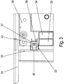
- Figure 3 shows a detailed view of the first variant of the converter.
- connection part 40 is fitted on the circuit board 38.
- the connecting section 42 is arranged to be electrically insulated from the housing part 32.
- the spacer section 33 functions as an insulating means.
- the spacing section 33 is preferably arranged at a distance from the housing part 32.
- the air gap between the spacing section 33 and the housing part 32 is smaller than 1 mm, preferably smaller than 0.5 mm.
- the converter therefore has no connecting means, in particular screw part 30, that connects housing part 32 and connecting part 40 to one another in an electrically conductive manner.
- the recess for the screw part 30 functions as a ventilation hole for the converter.
- connection part 40 is connected to the circuit board 38 using SMD technology by means of surface technology.
- the support section 37 of the connecting part 40 simultaneously functions as a connecting section 42.
Landscapes
- Engineering & Computer Science (AREA)
- Microelectronics & Electronic Packaging (AREA)
- Mounting Of Printed Circuit Boards And The Like (AREA)
- Inverter Devices (AREA)
- Connections Arranged To Contact A Plurality Of Conductors (AREA)
Description
- Die Erfindung betrifft ein Elektrogerät und ein Verfahren zur Herstellung eines Elektrogerätes.
- Aus der
DE 10 2012 005 622 A1 ist eine Schaltungsanordnung für einen Umrichter mit einer Filteranordnung bekannt. - Die
DE 10 2007 012 818 A1 zeigt eine Halbleitervorrichtung mit Anschlüssen. - In der
US 2010/0091464 A1 ist eine wärmeableitende Grundplattenstruktur, ein Modul aufweisend die wärmeableitende Grundplattenstruktur und ein Verfahren zur Herstellung der wärmeableitenden Grundplattenstruktur gezeigt. - Aus der
US 2013/0308257 A1 ist eine Substrateinheit bekannt. - Die
US 2009/0251843 A1 zeigt ein in einem Fahrzeug montiertes Elektrogerät und ein Fahrzeug, in dem das Elektrogerät montiert ist. - In der
US 2013/0265737 A1 sind ein Verfahren und ein Gerät zur Verhinderung von Lichtbogenüberschlägen in Motorsteuerungsgeräten gezeigt. - Aus der
DE 10 2012 005622 A1 ist eine Schaltungsanordnung und eine Anordnung von Kondensatoren bekannt. - Aus der
EP 2 416 484 A2 ist ein Matrixkonverter bekannt. - Aus der
US 2003/179594 A1 ist eine Anordnung zum Bewirken einer Basisinterferenz-Unterdrückung eines Matrixkonverters. - Aus der
EP 1 069 673 A1 ist ein Netzfilter bekannt. - Der Erfindung liegt daher die Aufgabe zugrunde, ein Elektrogerät und ein Verfahren zur Herstellung eines Elektrogerätes weiterzubilden, wobei die Sicherheit verbessert werden soll.
- Erfindungsgemäß wird die Aufgabe bei dem Elektrogerät nach den in Anspruch 1 angegebenen Merkmalen gelöst und bei dem Verfahren zur Herstellung eines Elektrogeräts nach den in Anspruch 13 angegebenen Merkmalen gelöst.
- Wichtige Merkmale der Erfindung bei dem Elektrogerät, insbesondere Umrichter, aufweisend eine Leiterplatte und ein Gehäuseteil, sind, dass
auf der Leiterplatte ein Anschlussteil bestückt ist, insbesondere lötverbunden ist,
wobei das Anschlussteil einen Beabstandungsabschnitt und einen Verbindungsabschnitt aufweist,
wobei die Leiterplatte mittels des Beabstandungsabschnitts von dem Gehäuseteil beabstandet ist,
wobei der Verbindungsabschnitt einen Gewindeabschnitt aufweist,
insbesondere wobei der Verbindungsabschnitt elektrisch leitend mit zumindest einer Leiterbahn auf der Leiterplatte verbunden ist. - Von Vorteil ist dabei, dass das Anschlussteil sicher mit der Leiterplatte verbindbar ist. Vorteilhafterweise ist das Anschlussteil in einem Arbeitsschritt mit weiteren Bauteilen auf der Leiterplatte bestückbar und in einem weiteren Arbeitsschritt mit den weiteren Bauteilen mit der Leiterplatte lötverbindbar. Somit ist der Umweltschutz verbessert.
- Vorteilhafterweise sind die Leiterplatte und auf der Leiterplatte bestückte elektrische Bauteile beabstandbar von dem Gehäuseteil mittels des Beabstandungsabschnitts. Somit ist die Durchschlagsfestigkeit des Elektrogerätes verbessert. Spannungsüberschläge von den elektrischen Bauteilen zu dem Gehäuseteil sind vermeidbar.
- Bei einer vorteilhaften Ausgestaltung ist das Anschlussteil als Verbundteil ausgeführt, wobei der Verbindungsabschnitt aus einem elektrisch leitenden Material hergestellt ist, insbesondere aus Metall hergestellt ist, wobei der Beabstandungsabschnitt aus einem elektrisch isolierenden Material hergestellt ist, insbesondere aus Kunststoff hergestellt ist. Von Vorteil ist dabei, dass das Anschlussteil mittels des Verbindungsabschnitts in einfacher Art und Weise mit der Leiterplatte lötverbindbar ist. Mittels des elektrisch isolierend ausgeführten Beabstandungsabschnitts sind die Leiterplatte und auf der Leiterplatte bestückte elektrische Bauteile von dem Gehäuseteil beabstandbar. Somit ist eine Luftstrecke zwischen der Leiterplatte mit den elektrischen Bauteilen und dem Gehäuseteil vorgebbar. Die Sicherheit des Elektrogerätes ist verbessert.
- Bei einer vorteilhaften Ausgestaltung ist der Beabstandungsabschnitt als Kunststoffspritzgussteil ausgeführt. Von Vorteil ist dabei, dass der Beabstandungsabschnitt in einfacher Art und Weise kostengünstig herstellbar ist.
- Bei einer vorteilhaften Ausgestaltung ist der Beabstandungsabschnitt angespritzt an den Verbindungsabschnitt. Von Vorteil ist dabei, dass der Beabstandungsabschnitt in einfacher Art und Weise sicher verbindbar ist mit dem Verbindungsabschnitt. Vorteilhafterweise ist der Beabstandungsabschnitt in einem einzigen Arbeitsschritt herstellbar und verbindbar mit dem Verbindungsabschnitt.
- Bei einer vorteilhaften Ausgestaltung ist der Verbindungsabschnitt zumindest teilweise überdeckt von dem Beabstandungsabschnitt. Von Vorteil ist dabei, dass der Beabstandungsabschnitt den Verbindungsabschnitt zumindest teilweise umgibt. Dadurch ist die Verbindung des Beabstandungsabschnitts mit dem Verbindungsabschnitt mechanisch stabil und sicher ausführbar.
- Bei einer vorteilhaften Ausgestaltung umgreift der Beabstandungsabschnitt eine Kante, insbesondere Blechkante, des Verbindungsabschnitts. Von Vorteil ist dabei, dass der Beabstandungsabschnitt die Kante des Verbindungsabschnitts zumindest teilweise umgibt. Somit sind die mechanische Stabilität und die Sicherheit der Verbindung des Beabstandungsabschnitts mit dem Verbindungsabschnitt verbessert.
- Bei einer vorteilhaften Ausgestaltung ist die Leiterplatte mit elektrischen Bauteilen bestückt, wobei der Beabstandungsabschnitt derart zwischen der Leiterplatte und dem Gehäuseteil angeordnet ist, dass die elektrischen Bauteile auf der Leiterplatte einen Mindestabstand zum Gehäuseteil aufweisen. Von Vorteil ist dabei, dass die Durchschlagfestigkeit des Elektrogerätes verbessert ist. Somit ist die Sicherheit des Elektrogerätes verbessert.
- Bei einer vorteilhaften Ausgestaltung ist der Abstand zwischen den elektrischen Bauteilen und dem Gehäuseteil, also die Luftstrecke, größer als 5 mm. Von Vorteil ist dabei, dass die Durchschlagspannung des Elektrogerätes größer als 10 kV ist. Somit ist ein sicherer Betrieb des Elektrogerätes auch bei hohen Betriebsspannungen ermöglicht.
- Bei einer vorteilhaften Ausgestaltung weist der Verbindungsabschnitt zumindest einen Anschlussabschnitt, insbesondere also ein Anschlussfüßchen, zumindest einen Auflageabschnitt und den Gewindeabschnitt auf. Von Vorteil ist dabei, dass der Verbindungsabschnitt kompakt ausführbar ist.
- Bei einer vorteilhaften Ausgestaltung ist der Verbindungsabschnitt einstückig ausgeführt. Von Vorteil ist dabei, dass der Verbindungsabschnitt kostengünstig fertigbar ist. Dabei sind Bauteile einsparbar, der Umweltschutz ist also verbessert.
- Bei einer vorteilhaften Ausgestaltung ist der Verbindungsabschnitt als Stanzbiegeteil ausgeführt, insbesondere als Stanzbiegeblechteil. Von Vorteil ist dabei, dass der Verbindungsabschnitt in einfacher Art und Weise fertigbar ist.
- Bei einer vorteilhaften Ausgestaltung ragt ein oder der Anschlussabschnitt durch eine Bohrung in der Leiterplatte hindurch und ist mit einer Leiterbahn der Leiterplatte lötverbunden. Von Vorteil ist dabei, dass das Anschlussteil im gleichen Arbeitsschritt wie die auf der Leiterplatte bestückten elektrischen Bauteile mit der Leiterplatte lötverbindbar ist.
- Bei einer vorteilhaften Ausgestaltung umgibt die senkrechte Projektion des Auflageabschnitts in die Leiterplattenebene die senkrechte Projektion der Bohrung in die Leiterplattenebene mit einem Winkel in Umfangsrichtung der Projektion der Bohrung von mehr als 180°, insbesondere mehr als 230°. Von Vorteil ist dabei, dass das Anschlussteil kippsicher auf der Leiterplatte anordenbar ist. Die Sicherheit beim Verlöten des Verbindungsabschnitts ist verbessert, da der Anschlussabschnitt oder die Anschlussabschnitte sicher in der Bohrung oder den Bohrungen angeordnet sind. Das Risiko eines Lötfehlers ist reduzierbar.
- Bei einer vorteilhaften Ausgestaltung erstreckt sich der Auflageabschnitt senkrecht zu einem Normalenvektor der Leiterplattenebene der Leiterplatte. Von Vorteil ist dabei, dass das Anschlussteil kippsicher auf der Leiterplatte anordenbar ist. Das Anschlussteil weist eine große der Leiterplatte zugewandte Oberfläche auf. Die der Leiterplatte zugewandte Oberfläche des Auflageabschnitts beträgt vorteilhafterweise mindestens 30 % der Gesamtoberfläche des Auflageabschnitts, insbesondere 40 %.
- Vorteilhafterweise ist ein Ausbrechen des mit der Leiterplatte lötverbundenen Anschlussteils verhinderbar.
- Bei einer vorteilhaften Ausgestaltung weist das Gehäuseteil ausgestanzte durch das Gehäuseteil durchgehende Ausnehmungen auf, wobei durch eine der Ausnehmungen ein Schraubteil hindurchführbar ist und/oder der Gewindeabschnitt fluchtend zu der Ausnehmung angeordnet ist, wobei mittels des Schraubteils das Gehäuseteil und der Verbindungsabschnitt elektrisch leitend verbindbar sind. Von Vorteil ist dabei, dass mittels des Schraubteils elektrische Bauteile auf der Leiterplatte mit dem Erdpotential verbindbar sind. Somit ist eine wahlweise Verbindung mit dem Erdpotential ermöglicht.
- Vorteilhafterweise ist das Elektrogerät anpassbar an verschiedene Anwendungen, die unterschiedliche Niederspannungsnetze zur elektrischen Stromversorgung erforderlich machen. Bei einem IT-System, das als erdfreies Netz ausgeführt ist, wird das Elektrogerät ohne Schraubteil verwendet, da die elektrischen Bauteile auf der Leiterplatte von dem geerdeten Gehäuseteil isoliert sein müssen. IT-Systeme werden in kleinen Netzen mit geringer Ausdehnung und hohen Anforderungen an die Fehlersicherheit verwendet, beispielsweise in Krankenhäusern. Es sind zusätzliche Schutzmaßnahmen zum Personenschutz erforderlich, wie beispielsweise Isolationsüberwachungseinrichtungen, Überstromschutzeinrichtungen, Fehlerstromschutzeinrichtungen und/oder Fehlerspannungsschutzeinrichtungen.
- Bei Niederspannungsnetzen mit Neutralleiter, wie beispielsweise TN-Systeme oder TT-Systeme, werden die elektrischen Bauteile teilweise mit dem Erdpotential verbunden. Dadurch sind Fehlerströme leichter zu erkennen als in einem IT-System, beispielsweise mittels Fehlerstromschutzschaltern. Die Niederspannungsnetze mit Neutralleiter sind also deutlich größer ausführbar als das IT-System.
- Die Ausnehmung für das Schraubteil ist vorteilhafterweise in einem Arbeitsschritt mit den weiteren Ausnehmungen, beispielsweise Belüftungslöcher, herstellbar.
- Vorteilhafterweise sind die elektrischen Bauteile mittels des Schraubteils mit dem geerdeten Gehäuseteil verbindbar. Somit ist das Elektrogerät sowohl für Netze mit Neutralleiter als auch für Netze ohne Neutralleiter verwendbar. Die Anpassung an das jeweilige Netz erfolgt in einfacher Art und Weise mittels Einschrauben des Schraubteils in das Anschlussteil beziehungsweise Lösen und Entfernen des Schraubteils.
- Bei einer vorteilhaften Ausgestaltung fungiert das Gehäuseteil als Erdanschluss. Von Vorteil ist dabei, dass das Elektrogerät kompakt ausführbar ist. Dabei sind Bauteile einsparbar. Der Umweltschutz ist verbessert.
- Bei einer vorteilhaften Ausgestaltung ist ein Schraubteil durch eine Ausnehmung im Gehäuseteil hindurchgeführt und mit dem Gewindeabschnitt schraubverbunden, insbesondere wobei diese Schraubverbindung selbstsichernd ausgeführt ist, wobei das Schraubteil das Gehäuseteil und den Verbindungsabschnitt elektrisch leitend verbindet. Von Vorteil ist dabei, dass die elektrisch leitende Verbindung zwischen dem Gehäuseteil und dem Verbindungsabschnitt in einfacher Art und Weise herstellbar ist. Diese Verbindung ist sicher ausführbar, wobei die Schraube schwingungssicher verbindbar ist.
- Bei einer vorteilhaften Ausgestaltung ist zwischen einem Schraubenkopf des Schraubteils und dem Gehäuseteil eine Lochscheibe angeordnet. Von Vorteil ist dabei, dass die Auflagefläche zwischen dem Schraubteil und dem Gehäuseteil vergrößerbar ist, somit ist die elektrische Leitfähigkeit verbessert.
- Bei einer vorteilhaften Ausgestaltung weist der Beabstandungsabschnitt eine Ausnehmung auf, durch welche das Schraubteil hindurchführbar, insbesondere hindurchgeführt, ist. Von Vorteil ist dabei, dass der Beabstandungsabschnitt zwischen dem Gehäuseteil und dem Verbindungsabschnitt einklemmbar ist. Dabei ist der Anpressdruck des Schraubteils gleichmäßig auf den das Schraubteil teilweise umgebenden Beabstandungsabschnitt verteilbar.
- Vorteilhafterweise fungiert der elastisch ausgeführte Beabstandungsabschnitt als mechanisches Dämpfungsmittel gegen Schwingungen des Gehäuseteils. Die Schwingungen des Gehäuseteils werden so gedämpft und die Leiterplatte ist schwingungsgedämpft im Gehäuse angeordnet.
- Bei einer vorteilhaften Ausgestaltung erstreckt die Ausnehmung sich durch den Beabstandungsabschnitt hindurch. Von Vorteil ist dabei, dass das Schraubteil hindurchführbar ist durch den Beabstandungsabschnitt.
- Bei einer vorteilhaften Ausgestaltung ist der Beabstandungsabschnitt im Wesentlichen U-förmig ausgeführt, wobei zwischen den Schenkeln des U ein Bereich des Schraubteils anordenbar, insbesondere angeordnet, ist. Von Vorteil ist dabei, dass Material einsparbar ist. Der Umweltschutz ist verbessert.
- Erfindungsgemäß sind auf der Leiterplatte erste Kapazitäten bestückt, wobei die ersten Kapazitäten einen gemeinsamen Sternpunkt aufweisen, wobei der Sternpunkt elektrisch leitend mit dem Verbindungsabschnitt des Anschlussteils verbunden ist, insbesondere mittels Leiterbahnen. Von Vorteil ist dabei, dass Fehlerströme der ersten Kapazitäten ableitbar sind mittels des Anschlussteils. Somit ist die Sicherheit des Elektrogerätes verbessert.
- Erfindungsgemäß ist der Sternpunkt mittels des Anschlussteils geerdet. Von Vorteil ist dabei, dass die Erdung in einfacher Art und Weise stabil und sicher ausführbar ist.
- Erfindungsgemäß sind auf der Leiterplatte erste Kapazitäten bestückt, wobei die ersten Kapazitäten einen gemeinsamen Sternpunkt aufweisen, wobei der Sternpunkt elektrisch leitend mit einer vierten Kapazität verbunden ist, wobei die vierte Kapazität mit dem Verbindungsabschnitt des Anschlussteils verbunden ist, insbesondere mittels zumindest einer Leiterbahn der Leiterplatte, wobei die vierte Kapazität elektrisch zwischen dem Sternpunkt und dem Anschlussteil angeordnet ist, insbesondere wobei der Sternpunkt, die vierte Kapazität und das Anschlussteil eine Reihenschaltung bilden. Von Vorteil ist dabei, dass die vierte Kapazität als zusätzliches Filter fungiert, mittels dessen hochfrequente Störströme ableitbar sind. Die Spannungsstabilität ist verbessert. Somit ist die Sicherheit des Elektrogerätes verbessert.
- Erfindungsgemäß ist die vierte Kapazität mittels des Anschlussteils geerdet. Von Vorteil ist dabei, dass Störströme zum Erdpotential ableitbar sind. Somit ist die Sicherheit des Elektrogerätes verbessert.
- Bei einer vorteilhaften Ausgestaltung sind auf der Leiterplatte zweite Kapazitäten bestückt, wobei die zweiten Kapazitäten eine Reihenschaltung bilden, die einen Mittelabgriff aufweist, insbesondere wobei der Mittelabgriff elektrisch leitend mit dem Sternpunkt verbunden ist. Von Vorteil ist dabei, dass ein hochfrequenter Potentialbezug zwischen einem Wechselspannungsabschnitt und einem Gleichspannungsabschnitt der Schaltung herstellbar ist. Mittels dieses Potentialbezugs sind Potentialsprünge zwischen dem Wechselspannungsabschnitt und dem Gleichspannungsabschnitt der Schaltung unterdrückbar. Diese Potentialsprünge entstehen aufgrund des Schaltmusters des Elektrogerätes.
- Bei einer vorteilhaften Ausgestaltung sind die zweiten Kapazitäten parallel geschaltet zu einer dritten Kapazität, insbesondere einem Zwischenkreiskondensator des Umrichters, angeordnet. Von Vorteil ist dabei, dass ein hochfrequenter Potentialbezug zwischen dem Zwischenkreis und dem Wechselspannungsabschnitt des Umrichters herstellbar ist. Somit ist der Erdanschluss über das Gehäuseteil entlastbar.
- Bei einer vorteilhaften Ausgestaltung weist das Elektrogerät einen mehrphasigen eingangsseitigen Wechselspannungsanschluss auf, der für jede Phase jeweils ein Anschlussmittel aufweist, wobei der Wechselspannungsanschluss einen Gleichrichter speist, wobei ein jeweiliges Anschlussmittel mittels einer jeweiligen Phasenleitung mit einem jeweiligen Eingangspol des Gleichrichters verbunden ist, wobei jede Phasenleitung jeweils einen Abgriff aufweist, wobei zwischen jedem Abgriff und dem Sternpunkt jeweils eine erste Kapazität elektrisch angeordnet ist. Von Vorteil ist dabei, dass die ersten Kapazitäten als Filtersystem für das Elektrogerät fungieren. Mittels der ersten Kapazitäten sind hochfrequente Fehlerströme ableitbar zum Sternpunkt. Somit ist die Sicherheit verbessert.
- Bei einer vorteilhaften Ausgestaltung weist das Elektrogerät einen Wechselrichter auf, wobei zwischen dem Gleichrichter und dem Wechselrichter ein Spannungszwischenkreis mit der dritten Kapazität als Zwischenkreiskondensator angeordnet ist, insbesondere wobei der Wechselrichter aus der dritten Kapazität gespeist ist. Von Vorteil ist dabei, dass das Elektrogerät als Umrichter ausführbar ist. Mittels des Umrichters ist ein Elektromotor speisbar, dessen Drehfrequenz mittels des Umrichters einstellbar ist.
- Bei einer vorteilhaften Ausgestaltung ist in jeder Phasenleitung zwischen dem jeweiligen Anschlussmittel und dem jeweiligen Abgriff für die jeweilige erste Kapazität eine jeweilige erste Induktivität angeordnet. Von Vorteil ist dabei, dass die ersten Kapazitäten und die ersten Induktivitäten einen Netzfilter für das Elektrogerät bilden. Somit ist die Sicherheit des Elektrogerätes verbessert.
- Bei einer vorteilhaften Ausgestaltung ist in jeder Phasenleitung zwischen dem jeweiligen Abgriff für die jeweilige erste Kapazität und dem jeweiligen Eingangspol des Gleichrichters eine jeweilige zweite Induktivität angeordnet. Von Vorteil ist dabei, dass die ersten Kapazitäten mit den zweiten Induktivitäten einen Netzfilter für das Elektrogerät bilden. Somit ist die Sicherheit des Elektrogerätes verbessert.
- Wichtige Merkmale der Erfindung bei dem Verfahren zur Herstellung eines Elektrogerätes, insbesondere wie zuvor beschrieben und/oder nach einem der auf das Elektrogerät gerichteten Schutzansprüche, einer Elektrogerätebaureihe, die mindestens zwei Varianten von Elektrogeräten aufweist, sind, dass
wahlweise eine erste oder eine zweite Variante hergestellt wird,
wobei in einem ersten Verfahrensschritt eine Leiterplatte mit zumindest einem Anschlussteil und Kondensatoren bestückt wird,
wobei die Kondensatoren einen gemeinsamen Sternpunkt aufweisen, insbesondere mit dem das Anschlussteil elektrisch leitend verbunden wird,
wobei in einem zweiten Verfahrensschritt die Leiterplatte in einem geerdeten Gehäuse mit einem Gehäuseteil angeordnet wird,
wobei der Sternpunkt bei der Herstellung der ersten Variante von dem geerdeten Gehäuse elektrisch isoliert ist,
wobei in einem optionalen dritten Verfahrensschritt zur Herstellung der zweiten Variante der Sternpunkt elektrisch leitend mit dem geerdeten Gehäuse verbunden wird, indem ein Verbindungsmittel, insbesondere ein Schraubteil, durch eine Ausnehmung in dem Gehäuseteil geführt und mit dem Anschlussteil lösbar verbunden wird. - Von Vorteil ist dabei, dass das Elektrogerät in einfacher Art und Weise anpassbar ist an den Betrieb in erdfreien Niederspannungsnetzen oder in Niederspannungsnetzen mit Neutralleiter.
- Vorteilhafterweise ist die Verbindung elektrischer Bauteile mit dem geerdeten Gehäuseteil lösbar ausführbar. Das Elektrogerät ist also nachträglich umrüstbar für den Betrieb in andersartigen Niederspannungsnetzen.
- Bei einer vorteilhaften Ausgestaltung wird beim dritten Verfahrensschritt das Schraubteil in das Anschlussteil eingeschraubt. Von Vorteil ist dabei, dass das Schraubteil in einfacher Art und Weise mit dem Anschlussteil verbindbar und lösbar ist. Vorteilhafterweise ist die Schraubverbindung selbstsichernd ausführbar. Somit ist das Schraubteil schwingungssicher mit dem Anschlussteil verbindbar.
- Bei einer vorteilhaften Ausgestaltung wird das Schraubteil mit dem geerdeten Gehäuseteil elektrisch leitend verbunden, insbesondere wobei das Schraubteil das Gehäuseteil berührt. Von Vorteil ist dabei, dass das Schraubteil als elektrisches Verbindungsmittel fungiert. Vorteilhafterweise weist das Schraubteil einen geringeren elektrischen Widerstand auf als Kabelverbindungen. Somit ist eine niederohmige Verbindung des geerdeten Gehäuseteils mit dem Anschlussteil ermöglicht. Die Sicherheit ist also verbessert.
- Weitere Vorteile ergeben sich aus den Unteransprüchen. Die Erfindung ist nicht auf die Merkmalskombination der Ansprüche beschränkt. Für den Fachmann ergeben sich weitere sinnvolle Kombinationsmöglichkeiten von Ansprüchen und/oder einzelnen Anspruchsmerkmalen und/oder Merkmalen der Beschreibung und/oder der Figuren, insbesondere aus der Aufgabenstellung und/oder der sich durch Vergleich mit dem Stand der Technik stellenden Aufgabe.
- Die Erfindung wird nun anhand von Abbildungen näher erläutert:
- In der
Figur 1 ist ein Prinzipschaltbild eines erfindungsgemäßen Elektrogeräts gezeichnet. -
Figur 2 zeigt eine Detailansicht eines erfindungsgemäßen Elektrogeräts in einer zweiten Variante in Draufsicht. -
Figur 3 zeigt eine Detailansicht des erfindungsgemäßen Elektrogeräts in einer ersten Variante in Draufsicht. - In der
Figur 4 ist eine Detailansicht des erfindungsgemäßen Elektrogeräts in der zweiten Variante in Schrägansicht gezeichnet, wobei ein Schraubteil explodiert dargestellt ist. - Das in
Figur 1 gezeigte Prinzipschaltbild zeigt das Elektrogerät, vorzugsweise einen Umrichter, mit einem dreiphasigen Wechselspannungsanschluss 1, einem Gleichrichter 5 und einem Wechselrichter 8. Der Wechselspannungsanschluss 1 weißt drei Anschlussmittel auf. In Reihe geschaltet zu jedem Anschlussmittel ist jeweils eine Induktivität (2, 3, 4) angeordnet. - Der Gleichrichter 5 weist den jeweiligen Phasen des Wechselstroms zugeordnete Eingangspole auf.
- Zwischen den Anschlussmitteln des Wechselspannungsanschlusses 1 und den Eingangspolen des Gleichrichters 5 weist jede Phase eine Phasenleitung auf.
- Zwischen der jeweiligen Induktivität (2, 3, 4) und dem Gleichrichter 5 weist jede Phase eine Abzweigung auf, die mit jeweils einer ersten Kapazität (14, 19, 20) verbunden ist. Die Kapazitäten (14, 19, 20) sind mit einem gemeinsamen Sternpunkt 18 verbunden. Der Sternpunkt 18 ist mit einer Erdverbindung verbindbar mittels eines zwischengeordneten Verbindungsmittels 16. Zwischen dem Verbindungsmittel 16 und dem Sternpunkt 18 ist eine vierte Kapazität 15 angeordnet.
- Im Spannungszwischenkreis zwischen dem Gleichrichter 5 und dem Wechselrichter 8 ist eine Reihenschaltung von zweiten Kapazitäten (6, 13) parallel geschaltet zu einer dritten Kapazität 11 angeordnet. Zwischen den zweiten Kapazitäten (6, 13) ist ein Mittelabgriff 7 angeordnet, der mit dem Sternpunkt 18 verbunden ist.
- Die zweiten Kapazitäten (6, 13) und die dritte Kapazität 11 sind also im Gleichspannungszwischenkreis angeordnet. Die dritte Kapazität 11 wird auch als Zwischenkreiskondensator bezeichnet.
- Die Bauteile des Umrichters sind in einem Gehäuse 10 angeordnet. Das Gehäuse 10 ist zumindest teilweise elektrisch leitend ausgeführt, vorzugsweise ist das Gehäuse 10 aus einem metallischen Material hergestellt. Das Gehäuse 10 ist mit einem Erdanschluss 12 elektrisch leitend verbunden und ist somit geerdet.
- Der Wechselrichter 8 ist ausgangsseitig mit einem Verbraucher verbunden, vorzugsweise ist der Verbraucher ein Motor M. Der Verbraucher weist ein Gehäuse auf, das mit einem Erdanschluss 9 elektrisch leitend verbunden ist, somit ist das Gehäuse des Verbrauchers geerdet.
- In
Figur 2 und4 ist eine Detailansicht der zweiten Variante des Umrichters gezeigt. Eine Leiterplatte 38 des Umrichters ist mit Kondensatoren (34, 35, 36) bestückt, die als Kapazitäten (14, 15, 19, 20) fungieren. - Die bestückte Leiterplatte 38 ist in einem Gehäuse angeordnet, das zumindest zwei Gehäuseteile (31, 32) aufweist. Das Gehäuseteil 32 weist zumindest eine Ausnehmung, insbesondere Bohrung, auf, durch welche ein Schraubteil 30 hindurchgeführt ist. Vorzugsweise ist zwischen dem Gehäuseteil 32 und einem Schraubkopf des Schraubteils 30 eine Lochscheibe 41 auf dem Schraubteil 30 angeordnet.
- Das Gehäuseteil 32 weist weitere Ausnehmungen 44 auf zur Belüftung des Umrichters, insbesondere also Belüftungslöcher. Diese Ausnehmungen 44 sind zumindest teilweise in einer Ebene mit der Ausnehmung für das Schraubteil 30 angeordnet.
- Vorzugsweise ist das Gehäuseteil 32 als Stanzbiegeteil ausgeführt, so dass die Ausnehmung für das Schraubteil 30 und die Ausnehmungen 44 zur Belüftung in einem Arbeitsschritt herstellbar sind. Die Ausnehmungen 44 sind also stanzbar.
- Auf der Leiterplatte 38 ist ein Anschlussteil 40 zur elektrisch leitenden Verbindung von zumindest einer mit den Kondensatoren (34, 35, 36) verbundenen Leiterbahn mit dem Gehäuseteil 32 bestückt. Das Anschlussteil 40 weist also zumindest einen Anschlussabschnitt 39 auf, der in eine Bohrung in der Leiterplatte 38 eingesteckt ist, lötverbunden und/oder mit der Leiterbahn elektrisch leitend verbunden ist. Vorzugsweise weist das Anschlussteil 40 zwei Anschlussabschnitte 39 auf.
- Mit dem Anschlussteil 40 ist das durch das Gehäuseteil 32 hindurchgeführte Schraubteil 30 verbunden, insbesondere auch elektrisch leitend verbunden. Dazu weist das Anschlussteil 40 einen Gewindeabschnitt 43 auf, in den das Schraubteil 30 eingeschraubt ist.
- Das Anschlussteil 40 weist einen Auflageabschnitt 37 auf. Dieser Auflageabschnitt 37 erstreckt sich senkrecht zum Normalenvektor der Leiterplattenebene der Leiterplatte 38 von einem Randbereich der Leiterplatte 38 in die Leiterplatte 38 hinein. Vorzugsweise ist der Auflageabschnitt 37 U-förmig ausgeführt. Vorzugsweise ist der Anschlussabschnitt 39 zwischen den Schenkeln des U-förmigen Auflageabschnittes 37 angeordnet. Dabei erstreckt sich der Anschlussabschnitt 39 vom Auflageabschnitt 37 aus.
- Die senkrechte Projektion des Auflageabschnitts 37 in die Leiterplattenebene umgibt die senkrechte Projektion der Bohrung in die Leiterplattenebene mit einem Winkel in Umfangsrichtung der Projektion der Bohrung von mehr als 180°, insbesondere mehr als 230°. Dieser Winkel ist der Umfangswinkel zum Schwerpunkt der Bohrung in der Leiterplatte 38.
- Die Leiterplatte 38 ist eben ausgeführt und weist Epoxidharz auf.
- Unter Leiterplattenebene versteht der Fachmann diejenige Ebene, die die Leiterplatte 38 bei verschwindender Leiterplattendicke aufweist.
- Das Anschlussteil 40 weist einen einstückigen Verbindungsabschnitt 42 auf, der den Gewindeabschnitt 43, den Anschlussabschnitt 39 und den Auflageabschnitt 37 aufweist. Der Verbindungsabschnitt 42 ist als Stanzbiegeteil ausgeführt, vorzugsweise als Stanzbiegeblechteil ausgeführt. Vorzugsweise ist der Verbindungsabschnitt 42 aus metallischem Material gefertigt. Somit ist der Verbindungsabschnitt 42 elektrisch leitend ausgeführt.
- In einem weiteren nicht dargestellten Ausführungsbeispiel weist der Verbindungsabschnitt 42 eine Ausnehmung auf, in der eine Gewindehülse aufgenommen ist, insbesondere verschweißt oder verlötet ist. Die Gewindehülse weist ein Innengewinde auf zur Verbindung mit dem Schraubteil 30.
- Das Anschlussteil 40 weist einen Beabstandungsabschnitt 33 auf. Der Beabstandungsabschnitt 33 beabstandet das Gehäuseteil 32 von dem Verbindungsabschnitt 42. Der Beabstandungsabschnitt 33 ist elektrisch isolierend ausgeführt. Vorzugsweise ist der Beabstandungsabschnitt 33 aus Kunststoff gefertigt, insbesondere als Kunststoffspritzgussteil. Vorzugsweise wird der Kunststoff an den Verbindungsabschnitt 42 angespritzt. Das Anschlussteil 40 ist ein Verbundteil, vorzugsweise ein Verbundteil aus Kunststoff und Metall.
- Der Beabstandungsabschnitt 33 weist eine Ausnehmung auf, durch welche das Schraubteil 30 hindurchführbar ist. Diese Ausnehmung ist als durchgehende Ausnehmung ausgeführt und erstreckt sich von dem Gewindeabschnitt 43 zu dem Gehäuseteil 32. Vorzugsweise ist der Beabstandungsabschnitt 33 U-förmig ausgeführt. Vorzugsweise ist ein Abschnitt des Schraubteils 30, vorzugsweise ein Gewindeabschnitt, zwischen den Schenkeln des U angeordnet.
- Der Abstand zwischen dem Verbindungsabschnitt 42 und dem Gehäuseteil 32 ist mindestens so groß wie die Luftstrecke zwischen der bestückten Leiterplatte 38 und dem Gehäuseteil 32. Somit verbessert der Beabstandungsabschnitt 33 die Durchschlagfestigkeit des Umrichters. Vorzugsweise beträgt der von dem Beabstandungsabschnitt 33 bewirkte Abstand zwischen der bestückten Leiterplatte 38 und dem Gehäuseteil 32, also die Luftstrecke, mindestens 5 mm, was einer Durchschlagspannung von mindestens 10 kV entspricht.
-
Figur 3 zeigt eine Detailansicht der ersten Variante des Umrichters. - Bei der ersten Variante ist wie bei der zweiten Variante das Anschlussteil 40 auf der Leiterplatte 38 bestückt. Dabei ist aber bei der ersten Variante der Verbindungsabschnitt 42 elektrisch isoliert von dem Gehäuseteil 32 angeordnet. Der Beabstandungsabschnitt 33 fungiert als Isoliermittel. Vorzugsweise ist der Beabstandungsabschnitt 33 beabstandet von dem Gehäuseteil 32 angeordnet. Dabei ist der Luftspalt zwischen dem Beabstandungsabschnitt 33 und dem Gehäuseteil 32 kleiner als 1 mm, vorzugsweise kleiner als 0,5 mm.
- Der Umrichter weist bei der ersten Variante also kein Verbindungsmittel, insbesondere Schraubteil 30, auf, dass das Gehäuseteil 32 und das Anschlussteil 40 elektrisch leitend miteinander verbindet. Dabei fungiert die Ausnehmung für das Schraubteil 30 als Belüftungsloch für den Umrichter.
- Bei einem weiteren nicht dargestellten erfindungsgemäßen Ausführungsbeispiel ist das Anschlussteil 40 in SMD-Technik mittels Oberflächentechnik mit der Leiterplatte 38 verbunden. Dazu fungiert der Auflageabschnitt 37 des Verbindungsteils 40 gleichzeitig als Verbindungsabschnitt 42.
-
- M Motor
- 1 Wechselspannungsanschluss
- 2 Induktivität
- 3 Induktivität
- 4 Induktivität
- 5 Gleichrichter
- 6 Kapazität
- 7 Mittelabgriff
- 8 Wechselrichter
- 9 Erdverbindung
- 10 Gehäuse
- 11 Kapazität
- 12 Erdverbindung
- 13 Kapazität
- 14 Kapazität
- 15 Kapazität
- 16 Verbindungsmittel
- 17 Erdverbindung
- 18 Sternpunkt
- 19 Kapazität
- 20 Kapazität
- 30 Schraubteil
- 31 Gehäuseteil
- 32 Gehäuseteil
- 33 Beabstandungsabschnitt
- 34 Kondensator
- 35 Kondensator
- 36 Kondensator
- 37 Auflageabschnitt
- 38 Leiterplatte
- 39 Anschlussabschnitt
- 40 Anschlussteil
- 41 Lochscheibe
- 42 Verbindungsabschnitt
- 43 Gewindeabschnitt
- 44 Ausnehmung
Claims (14)
- Elektrogerät, insbesondere Umrichter, aufweisend eine Leiterplatte (38) und ein Gehäuseteil (32),
wobei auf der Leiterplatte (38) ein Anschlussteil (40) bestückt ist, insbesondere lötverbunden ist,
wobei das Anschlussteil (40) einen Beabstandungsabschnitt (33) und einen Verbindungsabschnitt (42) aufweist,
wobei die Leiterplatte (38) mittels des Beabstandungsabschnitts (33) von dem Gehäuseteil (32) beabstandet ist,
wobei der Verbindungsabschnitt (42) einen Gewindeabschnitt (43) aufweist,
wobei der Verbindungsabschnitt (42) elektrisch leitend mit zumindest einer Leiterbahn auf der Leiterplatte (38) verbunden ist,
dadurch gekennzeichnet, dass
auf der Leiterplatte (38) erste Kapazitäten (14, 19, 20) bestückt sind,
wobei die ersten Kapazitäten (14, 19, 20) einen gemeinsamen Sternpunkt (18) aufweisen,
wobei der Sternpunkt (18) elektrisch leitend mit dem Verbindungsabschnitt (42) des Anschlussteils (40) mittels Leiterbahnen verbunden ist,
oder
wobei der Sternpunkt (18) elektrisch leitend mit einer vierten Kapazität (15) verbunden ist,
wobei die vierte Kapazität (15) mit dem Verbindungsabschnitt (42) des Anschlussteils (40) verbunden ist,
wobei die vierte Kapazität (15) elektrisch zwischen dem Sternpunkt (18) und dem Anschlussteil (40) angeordnet ist,
wobei das Gehäuseteil eine durchgehende Ausnehmung (44) aufweist,
wobei durch die Ausnehmung (44) ein Schraubteil (30) hindurchführbar ist und mit dem Gewindeabschnitt (43) schraubverbindbar ist,
wobei mittels des Schraubteils (30) das Gehäuseteil (32) und der Verbindungsabschnitt (42) elektrisch leitend verbindbar sind,
insbesondere wobei das Gehäuseteil (32) als Erdanschluss (17) fungiert. - Elektrogerät nach Anspruch 1,
dadurch gekennzeichnet, dass
das Anschlussteil (40) als Verbundteil ausgeführt ist,
wobei der Verbindungsabschnitt (42) aus einem elektrisch leitenden Material hergestellt ist, insbesondere aus Metall hergestellt ist,
wobei der Beabstandungsabschnitt (33) aus einem elektrisch isolierenden Material hergestellt ist, insbesondere aus Kunststoff hergestellt ist. - Elektrogerät nach mindestens einem der vorangegangenen Ansprüche,
dadurch gekennzeichnet, dass
der Beabstandungsabschnitt (33) als Kunststoffspritzgussteil ausgeführt ist,
insbesondere wobei der Beabstandungsabschnitt (33) angespritzt ist an den Verbindungsabschnitt (42),
insbesondere wobei der Verbindungsabschnitt (42) zumindest teilweise überdeckt ist von dem Beabstandungsabschnitt (33) und/oder der Beabstandungsabschnitt (33) eine Kante, insbesondere Blechkante, des Verbindungsabschnitts (42) umgreift. - Elektrogerät nach mindestens einem der vorangegangenen Ansprüche,
dadurch gekennzeichnet, dass
die Leiterplatte (38) mit elektrischen Bauteilen bestückt ist,
wobei der Beabstandungsabschnitt (33) derart zwischen der Leiterplatte (38) und dem Gehäuseteil (32) angeordnet ist, dass die elektrischen Bauteile auf der Leiterplatte (38) einen Mindestabstand zum Gehäuseteil (32) aufweisen,
insbesondere wobei der Abstand zwischen den elektrischen Bauteilen und dem Gehäuseteil (32), also die Luftstrecke, größer ist als 5 mm. - Elektrogerät nach mindestens einem der vorangegangenen Ansprüche,
dadurch gekennzeichnet, dass
der Verbindungsabschnitt (42)- zumindest einen Anschlussabschnitt (39), insbesondere also ein Anschlussfüßchen,- zumindest einen Auflageabschnitt (37) und- den Gewindeabschnitt (43)aufweist,
insbesondere wobei der Verbindungsabschnitt (42) einstückig ausgeführt ist,
insbesondere wobei der Verbindungsabschnitt (42) als Stanzbiegeteil ausgeführt ist, insbesondere als Stanzbiegeblechteil. - Elektrogerät nach mindestens einem der vorangegangenen Ansprüche,
dadurch gekennzeichnet, dass
ein oder der Anschlussabschnitt (39) durch eine Bohrung in der Leiterplatte (38) hindurchragt und mit einer Leiterbahn der Leiterplatte (38) lötverbunden ist,
insbesondere wobei die senkrechte Projektion des Auflageabschnitts (39) in die Leiterplattenebene die senkrechte Projektion der Bohrung in die Leiterplattenebene umgibt mit einem Winkel in Umfangsrichtung der Projektion der Bohrung von mehr als 180°, insbesondere mehr als 230°,
und/oder dass
der Auflageabschnitt (37) sich senkrecht zu einem Normalenvektor der Leiterplattenebene der Leiterplatte (38) erstreckt. - Elektrogerät nach mindestens einem der vorangegangenen Ansprüche,
dadurch gekennzeichnet, dass
das Schraubteil (30) durch die Ausnehmung (44) im Gehäuseteil (32) hindurchgeführt ist und mit dem Gewindeabschnitt (43) schraubverbunden ist, wobei diese Schraubverbindung selbstsichernd ausgeführt ist,
wobei das Schraubteil (30) das Gehäuseteil (32) und den Verbindungsabschnitt (42) elektrisch leitend verbindet,
insbesondere wobei das Gehäuseteil (32) als Erdanschluss (17) fungiert,
insbesondere wobei zwischen einem Schraubenkopf des Schraubteils (30) und dem Gehäuseteil (32) eine Lochscheibe (41) angeordnet ist. - Elektrogerät nach mindestens einem der vorangegangenen Ansprüche,
dadurch gekennzeichnet, dass
der Beabstandungsabschnitt (33) eine Ausnehmung aufweist, durch welche das Schraubteil (30) hindurchführbar, insbesondere hindurchgeführt, ist,
insbesondere wobei die Ausnehmung sich durch den Beabstandungsabschnitt (33) hindurch erstreckt,
insbesondere wobei der Beabstandungsabschnitt (33) im Wesentlichen U-förmig ausgeführt ist, wobei zwischen den Schenkeln des U ein Bereich des Schraubteils (30) anordenbar, insbesondere angeordnet, ist. - Elektrogerät nach mindestens einem der vorangegangenen Ansprüche, dadurch gekennzeichnet, dass der Sternpunkt (18) mittels des Anschlussteils (40) geerdet ist, oder dass die vierte Kapazität (15) mittels des Anschlussteils (40) geerdet ist.
- Elektrogerät nach mindestens einem der vorangegangenen Ansprüche,
dadurch gekennzeichnet, dass
auf der Leiterplatte (38) zweite Kapazitäten (6, 13) bestückt sind,
wobei die zweiten Kapazitäten (6, 13) eine Reihenschaltung bilden, die einen Mittelabgriff (7) aufweist,
insbesondere wobei der Mittelabgriff (7) elektrisch leitend mit dem Sternpunkt (18) verbunden ist,
und/oder dass
die zweiten Kapazitäten (6, 13) parallel geschaltet zu einer dritten Kapazität (11), insbesondere einem Zwischenkreiskondensator des Umrichters, angeordnet sind. - Elektrogerät nach mindestens einem der vorangegangenen Ansprüche,
dadurch gekennzeichnet, dass
das Elektrogerät einen mehrphasigen eingangsseitigen Wechselspannungsanschluss (1), der für jede Phase jeweils ein Anschlussmittel aufweist, aufweist,
wobei der Wechselspannungsanschluss (1) einen Gleichrichter (5) speist,
wobei das jeweilige Anschlussmittel mittels einer jeweiligen Phasenleitung mit einem jeweiligen Eingangspol des Gleichrichters (5) verbunden ist,
wobei jede Phasenleitung jeweils einen Abgriff aufweist,
wobei zwischen jedem Abgriff und dem Sternpunkt (18) jeweils eine erste Kapazität (15) elektrisch angeordnet ist. - Elektrogerät nach mindestens einem der vorangegangenen Ansprüche,
dadurch gekennzeichnet, dass
das Elektrogerät einen Wechselrichter (8) aufweist,
wobei zwischen dem Gleichrichter (5) und dem Wechselrichter (8) ein Spannungszwischenkreis mit der dritten Kapazität (11) als Zwischenkreiskondensator angeordnet ist, insbesondere wobei der Wechselrichter (8) aus der dritten Kapazität (11) gespeist ist,
und/oder dass
in jeder Phasenleitung zwischen dem jeweiligen Anschlussmittel und dem jeweiligen Abgriff für die jeweilige erste Kapazität (14, 19, 20) eine jeweilige erste Induktivität (2, 3, 4) angeordnet ist,
und/oder dass
in jeder Phasenleitung zwischen dem jeweiligen Abgriff für die jeweilige erste Kapazität (14, 19, 20) und dem jeweiligen Eingangspol des Gleichrichters (5) eine jeweilige zweite Induktivität angeordnet ist. - Verfahren zur Herstellung eines Elektrogerätes nach mindestens einem der vorangegangenen Ansprüche, einer Elektrogerätebaureihe, die mindestens zwei Varianten von Elektrogeräten aufweist,
dadurch gekennzeichnet, dass
wahlweise eine erste oder eine zweite Variante hergestellt wird,
wobei in einem ersten Verfahrensschritt eine Leiterplatte (38) mit zumindest einem Anschlussteil (40) und als Kapazitäten (14, 15, 19, 20) fungierende Kondensatoren (34, 35, 36) bestückt wird,
wobei die Kondensatoren (34, 35, 36) einen gemeinsamen Sternpunkt (18) aufweisen, insbesondere mit dem das Anschlussteil (40) elektrisch leitend verbunden wird,
wobei in einem zweiten Verfahrensschritt die Leiterplatte (38) in einem geerdeten Gehäuse (10) mit einem Gehäuseteil (32) angeordnet wird,
wobei der Sternpunkt (18) bei der Herstellung der ersten Variante von dem geerdeten Gehäuse (10) elektrisch isoliert ist,
wobei in einem optionalen dritten Verfahrensschritt zur Herstellung der zweiten Variante der Sternpunkt (18) elektrisch leitend mit dem geerdeten Gehäuse (10) verbunden wird, indem ein Verbindungsmittel, insbesondere ein Schraubteil (30), durch eine Ausnehmung in dem Gehäuseteil (32) geführt und mit dem Anschlussteil (40) lösbar verbunden wird. - Verfahren nach Anspruch 13,
dadurch gekennzeichnet, dass
beim dritten Verfahrensschritt das Schraubteil (30) in das Anschlussteil (40) eingeschraubt wird,
insbesondere wobei das Schraubteil (30) mit dem geerdeten Gehäuseteil (32) elektrisch leitend verbunden wird, insbesondere wobei das Schraubteil (30) das Gehäuseteil (32) berührt.
Applications Claiming Priority (2)
| Application Number | Priority Date | Filing Date | Title |
|---|---|---|---|
| DE102014004799.7A DE102014004799B4 (de) | 2014-04-03 | 2014-04-03 | Elektrogerät und Verfahren zur Herstellung eines Elektrogerätes |
| PCT/EP2015/000502 WO2015149907A1 (de) | 2014-04-03 | 2015-03-06 | Elektrogerät und verfahren zur herstellung eines elektrogerätes |
Publications (2)
| Publication Number | Publication Date |
|---|---|
| EP3127406A1 EP3127406A1 (de) | 2017-02-08 |
| EP3127406B1 true EP3127406B1 (de) | 2021-02-24 |
Family
ID=52669574
Family Applications (1)
| Application Number | Title | Priority Date | Filing Date |
|---|---|---|---|
| EP15709414.5A Active EP3127406B1 (de) | 2014-04-03 | 2015-03-06 | Elektrogerät und verfahren zur herstellung eines elektrogerätes |
Country Status (6)
| Country | Link |
|---|---|
| US (1) | US10076052B2 (de) |
| EP (1) | EP3127406B1 (de) |
| CN (1) | CN106165555B (de) |
| AU (1) | AU2015240092B2 (de) |
| DE (1) | DE102014004799B4 (de) |
| WO (1) | WO2015149907A1 (de) |
Families Citing this family (6)
| Publication number | Priority date | Publication date | Assignee | Title |
|---|---|---|---|---|
| DE102014010979B3 (de) | 2014-07-29 | 2015-11-05 | Sew-Eurodrive Gmbh & Co Kg | Verwendung eines Anzeigemittels eines Umrichters, Verfahren zum Betreiben eines Umrichters und Umrichter |
| FR3071695B1 (fr) * | 2017-09-27 | 2021-10-22 | Valeo Japan Co Ltd | Compresseur pour installation de conditionnement d'air pour vehicule automobile |
| CN109659923A (zh) * | 2018-12-20 | 2019-04-19 | 威创集团股份有限公司 | 一种用于电子电气设备的接地结构及电子电气设备 |
| DE102019218210B4 (de) | 2019-11-25 | 2022-12-29 | Lenze Swiss Ag | Elektrisches Gerät |
| DE102021005368A1 (de) | 2020-11-18 | 2022-05-19 | Sew-Eurodrive Gmbh & Co Kg | Elektrogerät und Anordnung von Elektrogeräten |
| DE102021214906A1 (de) | 2021-10-14 | 2023-04-20 | Vitesco Technologies Germany Gmbh | Elektronische Baugruppe |
Citations (4)
| Publication number | Priority date | Publication date | Assignee | Title |
|---|---|---|---|---|
| EP1069673A1 (de) * | 1999-07-16 | 2001-01-17 | Schaffner Emv Ag | Netzfilter |
| US20030179594A1 (en) * | 2000-08-16 | 2003-09-25 | Manfred Bruckmann | Device for effecting the basic interference suppression of a matrix converter |
| EP2416484A2 (de) * | 2010-07-20 | 2012-02-08 | Kabushiki Kaisha Yaskawa Denki | Matrixwandler |
| DE102012005622A1 (de) * | 2012-03-22 | 2013-09-26 | Sew-Eurodrive Gmbh & Co. Kg | Schaltungsanordnung und Anordnung von Kondensatoren |
Family Cites Families (18)
| Publication number | Priority date | Publication date | Assignee | Title |
|---|---|---|---|---|
| US4254301A (en) * | 1979-03-19 | 1981-03-03 | Xerox Corporation | Printed circuit board component mounting support and spacer |
| US5008777A (en) * | 1988-10-14 | 1991-04-16 | At&T Bell Laboratories | Auxiliary board spacer arrangement |
| JP2933845B2 (ja) | 1995-02-17 | 1999-08-16 | 三菱電機株式会社 | 印刷回路基板取付装置 |
| US6186800B1 (en) * | 1999-01-13 | 2001-02-13 | Micron Electronics, Inc. | Circuit board grounding and support structure |
| US6863562B1 (en) * | 2003-08-21 | 2005-03-08 | International Business Machines Corporation | Pin mounted circuit board retainer |
| WO2005072033A1 (ja) * | 2004-01-27 | 2005-08-04 | Matsushita Electric Industrial Co., Ltd. | 回路基板およびチップ部品実装方法 |
| JP2005216884A (ja) * | 2004-01-27 | 2005-08-11 | Matsushita Electric Ind Co Ltd | 回路基板およびチップ部品実装方法 |
| JP4577276B2 (ja) * | 2006-06-07 | 2010-11-10 | トヨタ自動車株式会社 | 車載用電子装置およびそれを搭載する車両 |
| JP4242401B2 (ja) | 2006-06-29 | 2009-03-25 | 三菱電機株式会社 | 半導体装置 |
| JP4941555B2 (ja) | 2007-11-30 | 2012-05-30 | パナソニック株式会社 | 放熱構造体基板 |
| JP4450104B2 (ja) * | 2008-04-30 | 2010-04-14 | ダイキン工業株式会社 | 接続部材の取付構造及び冷凍装置 |
| DE102008031296A1 (de) | 2008-07-02 | 2009-08-20 | Siemens Aktiengesellschaft | Drosselspuleneinrichtung für einen Filterschaltkreis sowie Verwendung einer solchen und Filterschaltkreis |
| US8134838B2 (en) | 2008-07-21 | 2012-03-13 | Infineon Technologies Ag | Semiconductor module and method |
| US8295054B2 (en) | 2009-04-06 | 2012-10-23 | Fsp Technology Inc. | Printed circuit board fastening structure |
| JP5516822B2 (ja) * | 2011-03-16 | 2014-06-11 | トヨタ自動車株式会社 | 基板ユニット |
| US9237663B2 (en) * | 2012-04-06 | 2016-01-12 | Rockwell Automation Technologies, Inc. | Methods and apparatus for mitigating arc flash incident energy in motor control devices |
| US9355790B2 (en) * | 2013-06-27 | 2016-05-31 | Intel Corporation | Energy storage devices having enhanced specific energy and associated methods |
| US9859810B2 (en) * | 2013-11-20 | 2018-01-02 | Nissan Motor Co., Ltd. | Power converter |
-
2014
- 2014-04-03 DE DE102014004799.7A patent/DE102014004799B4/de active Active
-
2015
- 2015-03-06 CN CN201580016600.XA patent/CN106165555B/zh active Active
- 2015-03-06 EP EP15709414.5A patent/EP3127406B1/de active Active
- 2015-03-06 AU AU2015240092A patent/AU2015240092B2/en active Active
- 2015-03-06 WO PCT/EP2015/000502 patent/WO2015149907A1/de not_active Ceased
- 2015-03-06 US US15/301,687 patent/US10076052B2/en active Active
Patent Citations (4)
| Publication number | Priority date | Publication date | Assignee | Title |
|---|---|---|---|---|
| EP1069673A1 (de) * | 1999-07-16 | 2001-01-17 | Schaffner Emv Ag | Netzfilter |
| US20030179594A1 (en) * | 2000-08-16 | 2003-09-25 | Manfred Bruckmann | Device for effecting the basic interference suppression of a matrix converter |
| EP2416484A2 (de) * | 2010-07-20 | 2012-02-08 | Kabushiki Kaisha Yaskawa Denki | Matrixwandler |
| DE102012005622A1 (de) * | 2012-03-22 | 2013-09-26 | Sew-Eurodrive Gmbh & Co. Kg | Schaltungsanordnung und Anordnung von Kondensatoren |
Also Published As
| Publication number | Publication date |
|---|---|
| DE102014004799B4 (de) | 2022-05-19 |
| US10076052B2 (en) | 2018-09-11 |
| US20170118857A1 (en) | 2017-04-27 |
| WO2015149907A1 (de) | 2015-10-08 |
| CN106165555B (zh) | 2019-03-29 |
| AU2015240092A1 (en) | 2016-10-20 |
| CN106165555A (zh) | 2016-11-23 |
| DE102014004799A1 (de) | 2015-10-08 |
| AU2015240092B2 (en) | 2019-04-04 |
| EP3127406A1 (de) | 2017-02-08 |
Similar Documents
| Publication | Publication Date | Title |
|---|---|---|
| EP3127406B1 (de) | Elektrogerät und verfahren zur herstellung eines elektrogerätes | |
| DE102017108383B4 (de) | Filter mit Leiterplatte und Stromschienen | |
| DE102012005622B4 (de) | Schaltungsanordnung | |
| DE102007049667B4 (de) | Anordnung und Verfahren zur Kompensation eines Fehlerstromes bei einem Erdschluss | |
| EP3906609B1 (de) | Elektrische maschine | |
| EP3446384B1 (de) | Antriebssystem mit einer zwischenkreisverschienung | |
| EP2905888A1 (de) | Stromrichter | |
| EP3459170B1 (de) | Vorrichtung zur elektrischen verbindung von mindestens einem elektrischen bauelement mit einer ersten und zweiten stromschiene | |
| EP2940702A1 (de) | Differenzstrom-messmodul | |
| EP2523296A1 (de) | Schaltungsanordnung zum Bereitstellen eines Überspannungsschutzes und Verfahren zu deren Betrieb | |
| WO2024165263A1 (de) | Ladestecker-anschlussvorrichtung | |
| EP3251474B1 (de) | Elektrogerät | |
| DE102014004800A1 (de) | Elektrogerät und Verfahren zur Herstellung | |
| EP3369139B1 (de) | Anschlusseinheit für ein elektrogerät, elektrogerätesystem und verfahren zur herstellung | |
| DE102007006840B3 (de) | Dämpfungselement | |
| DE102018000961A1 (de) | Elektronische Anordnung mit Leistungsmodul, Leiterplatte und Kühlkörper | |
| DE102019133954B4 (de) | Anordnung zur Filterung von Störungen | |
| DE102015107188A1 (de) | Leistungselektronikeinrichtung | |
| DE102022002105A1 (de) | Gerät mit Verbindungsanordnung | |
| DE102024106869A1 (de) | Elektromotor | |
| EP2976931A1 (de) | Stromschienenanordnung und verfahren zur herstellung einer stromschienenanordnung |
Legal Events
| Date | Code | Title | Description |
|---|---|---|---|
| STAA | Information on the status of an ep patent application or granted ep patent |
Free format text: STATUS: THE INTERNATIONAL PUBLICATION HAS BEEN MADE |
|
| PUAI | Public reference made under article 153(3) epc to a published international application that has entered the european phase |
Free format text: ORIGINAL CODE: 0009012 |
|
| STAA | Information on the status of an ep patent application or granted ep patent |
Free format text: STATUS: REQUEST FOR EXAMINATION WAS MADE |
|
| 17P | Request for examination filed |
Effective date: 20161103 |
|
| AK | Designated contracting states |
Kind code of ref document: A1 Designated state(s): AL AT BE BG CH CY CZ DE DK EE ES FI FR GB GR HR HU IE IS IT LI LT LU LV MC MK MT NL NO PL PT RO RS SE SI SK SM TR |
|
| AX | Request for extension of the european patent |
Extension state: BA ME |
|
| DAV | Request for validation of the european patent (deleted) | ||
| DAX | Request for extension of the european patent (deleted) | ||
| STAA | Information on the status of an ep patent application or granted ep patent |
Free format text: STATUS: EXAMINATION IS IN PROGRESS |
|
| 17Q | First examination report despatched |
Effective date: 20190617 |
|
| GRAP | Despatch of communication of intention to grant a patent |
Free format text: ORIGINAL CODE: EPIDOSNIGR1 |
|
| STAA | Information on the status of an ep patent application or granted ep patent |
Free format text: STATUS: GRANT OF PATENT IS INTENDED |
|
| INTG | Intention to grant announced |
Effective date: 20201006 |
|
| RIN1 | Information on inventor provided before grant (corrected) |
Inventor name: NIKOLA, JOACHIM Inventor name: KOLLAR, HANS JUERGEN Inventor name: MOMANN, DIRK |
|
| GRAS | Grant fee paid |
Free format text: ORIGINAL CODE: EPIDOSNIGR3 |
|
| GRAA | (expected) grant |
Free format text: ORIGINAL CODE: 0009210 |
|
| STAA | Information on the status of an ep patent application or granted ep patent |
Free format text: STATUS: THE PATENT HAS BEEN GRANTED |
|
| AK | Designated contracting states |
Kind code of ref document: B1 Designated state(s): AL AT BE BG CH CY CZ DE DK EE ES FI FR GB GR HR HU IE IS IT LI LT LU LV MC MK MT NL NO PL PT RO RS SE SI SK SM TR |
|
| REG | Reference to a national code |
Ref country code: GB Ref legal event code: FG4D Free format text: NOT ENGLISH |
|
| REG | Reference to a national code |
Ref country code: CH Ref legal event code: EP |
|
| REG | Reference to a national code |
Ref country code: DE Ref legal event code: R096 Ref document number: 502015014287 Country of ref document: DE |
|
| REG | Reference to a national code |
Ref country code: AT Ref legal event code: REF Ref document number: 1366132 Country of ref document: AT Kind code of ref document: T Effective date: 20210315 |
|
| REG | Reference to a national code |
Ref country code: IE Ref legal event code: FG4D Free format text: LANGUAGE OF EP DOCUMENT: GERMAN |
|
| REG | Reference to a national code |
Ref country code: LT Ref legal event code: MG9D |
|
| REG | Reference to a national code |
Ref country code: NL Ref legal event code: MP Effective date: 20210224 |
|
| PG25 | Lapsed in a contracting state [announced via postgrant information from national office to epo] |
Ref country code: PT Free format text: LAPSE BECAUSE OF FAILURE TO SUBMIT A TRANSLATION OF THE DESCRIPTION OR TO PAY THE FEE WITHIN THE PRESCRIBED TIME-LIMIT Effective date: 20210624 Ref country code: LT Free format text: LAPSE BECAUSE OF FAILURE TO SUBMIT A TRANSLATION OF THE DESCRIPTION OR TO PAY THE FEE WITHIN THE PRESCRIBED TIME-LIMIT Effective date: 20210224 Ref country code: FI Free format text: LAPSE BECAUSE OF FAILURE TO SUBMIT A TRANSLATION OF THE DESCRIPTION OR TO PAY THE FEE WITHIN THE PRESCRIBED TIME-LIMIT Effective date: 20210224 Ref country code: GR Free format text: LAPSE BECAUSE OF FAILURE TO SUBMIT A TRANSLATION OF THE DESCRIPTION OR TO PAY THE FEE WITHIN THE PRESCRIBED TIME-LIMIT Effective date: 20210525 Ref country code: HR Free format text: LAPSE BECAUSE OF FAILURE TO SUBMIT A TRANSLATION OF THE DESCRIPTION OR TO PAY THE FEE WITHIN THE PRESCRIBED TIME-LIMIT Effective date: 20210224 Ref country code: BG Free format text: LAPSE BECAUSE OF FAILURE TO SUBMIT A TRANSLATION OF THE DESCRIPTION OR TO PAY THE FEE WITHIN THE PRESCRIBED TIME-LIMIT Effective date: 20210524 Ref country code: NO Free format text: LAPSE BECAUSE OF FAILURE TO SUBMIT A TRANSLATION OF THE DESCRIPTION OR TO PAY THE FEE WITHIN THE PRESCRIBED TIME-LIMIT Effective date: 20210524 |
|
| PG25 | Lapsed in a contracting state [announced via postgrant information from national office to epo] |
Ref country code: SE Free format text: LAPSE BECAUSE OF FAILURE TO SUBMIT A TRANSLATION OF THE DESCRIPTION OR TO PAY THE FEE WITHIN THE PRESCRIBED TIME-LIMIT Effective date: 20210224 Ref country code: RS Free format text: LAPSE BECAUSE OF FAILURE TO SUBMIT A TRANSLATION OF THE DESCRIPTION OR TO PAY THE FEE WITHIN THE PRESCRIBED TIME-LIMIT Effective date: 20210224 Ref country code: PL Free format text: LAPSE BECAUSE OF FAILURE TO SUBMIT A TRANSLATION OF THE DESCRIPTION OR TO PAY THE FEE WITHIN THE PRESCRIBED TIME-LIMIT Effective date: 20210224 Ref country code: NL Free format text: LAPSE BECAUSE OF FAILURE TO SUBMIT A TRANSLATION OF THE DESCRIPTION OR TO PAY THE FEE WITHIN THE PRESCRIBED TIME-LIMIT Effective date: 20210224 Ref country code: LV Free format text: LAPSE BECAUSE OF FAILURE TO SUBMIT A TRANSLATION OF THE DESCRIPTION OR TO PAY THE FEE WITHIN THE PRESCRIBED TIME-LIMIT Effective date: 20210224 |
|
| PG25 | Lapsed in a contracting state [announced via postgrant information from national office to epo] |
Ref country code: IS Free format text: LAPSE BECAUSE OF FAILURE TO SUBMIT A TRANSLATION OF THE DESCRIPTION OR TO PAY THE FEE WITHIN THE PRESCRIBED TIME-LIMIT Effective date: 20210624 |
|
| PG25 | Lapsed in a contracting state [announced via postgrant information from national office to epo] |
Ref country code: EE Free format text: LAPSE BECAUSE OF FAILURE TO SUBMIT A TRANSLATION OF THE DESCRIPTION OR TO PAY THE FEE WITHIN THE PRESCRIBED TIME-LIMIT Effective date: 20210224 Ref country code: CZ Free format text: LAPSE BECAUSE OF FAILURE TO SUBMIT A TRANSLATION OF THE DESCRIPTION OR TO PAY THE FEE WITHIN THE PRESCRIBED TIME-LIMIT Effective date: 20210224 Ref country code: SM Free format text: LAPSE BECAUSE OF FAILURE TO SUBMIT A TRANSLATION OF THE DESCRIPTION OR TO PAY THE FEE WITHIN THE PRESCRIBED TIME-LIMIT Effective date: 20210224 |
|
| REG | Reference to a national code |
Ref country code: CH Ref legal event code: PL |
|
| REG | Reference to a national code |
Ref country code: DE Ref legal event code: R097 Ref document number: 502015014287 Country of ref document: DE |
|
| PG25 | Lapsed in a contracting state [announced via postgrant information from national office to epo] |
Ref country code: MC Free format text: LAPSE BECAUSE OF FAILURE TO SUBMIT A TRANSLATION OF THE DESCRIPTION OR TO PAY THE FEE WITHIN THE PRESCRIBED TIME-LIMIT Effective date: 20210224 Ref country code: DK Free format text: LAPSE BECAUSE OF FAILURE TO SUBMIT A TRANSLATION OF THE DESCRIPTION OR TO PAY THE FEE WITHIN THE PRESCRIBED TIME-LIMIT Effective date: 20210224 Ref country code: ES Free format text: LAPSE BECAUSE OF FAILURE TO SUBMIT A TRANSLATION OF THE DESCRIPTION OR TO PAY THE FEE WITHIN THE PRESCRIBED TIME-LIMIT Effective date: 20210224 Ref country code: SK Free format text: LAPSE BECAUSE OF FAILURE TO SUBMIT A TRANSLATION OF THE DESCRIPTION OR TO PAY THE FEE WITHIN THE PRESCRIBED TIME-LIMIT Effective date: 20210224 Ref country code: RO Free format text: LAPSE BECAUSE OF FAILURE TO SUBMIT A TRANSLATION OF THE DESCRIPTION OR TO PAY THE FEE WITHIN THE PRESCRIBED TIME-LIMIT Effective date: 20210224 |
|
| REG | Reference to a national code |
Ref country code: BE Ref legal event code: MM Effective date: 20210331 |
|
| PLBE | No opposition filed within time limit |
Free format text: ORIGINAL CODE: 0009261 |
|
| STAA | Information on the status of an ep patent application or granted ep patent |
Free format text: STATUS: NO OPPOSITION FILED WITHIN TIME LIMIT |
|
| GBPC | Gb: european patent ceased through non-payment of renewal fee |
Effective date: 20210524 |
|
| PG25 | Lapsed in a contracting state [announced via postgrant information from national office to epo] |
Ref country code: LU Free format text: LAPSE BECAUSE OF NON-PAYMENT OF DUE FEES Effective date: 20210306 Ref country code: LI Free format text: LAPSE BECAUSE OF NON-PAYMENT OF DUE FEES Effective date: 20210331 Ref country code: AL Free format text: LAPSE BECAUSE OF FAILURE TO SUBMIT A TRANSLATION OF THE DESCRIPTION OR TO PAY THE FEE WITHIN THE PRESCRIBED TIME-LIMIT Effective date: 20210224 Ref country code: CH Free format text: LAPSE BECAUSE OF NON-PAYMENT OF DUE FEES Effective date: 20210331 Ref country code: IE Free format text: LAPSE BECAUSE OF NON-PAYMENT OF DUE FEES Effective date: 20210306 |
|
| 26N | No opposition filed |
Effective date: 20211125 |
|
| PG25 | Lapsed in a contracting state [announced via postgrant information from national office to epo] |
Ref country code: SI Free format text: LAPSE BECAUSE OF FAILURE TO SUBMIT A TRANSLATION OF THE DESCRIPTION OR TO PAY THE FEE WITHIN THE PRESCRIBED TIME-LIMIT Effective date: 20210224 |
|
| PG25 | Lapsed in a contracting state [announced via postgrant information from national office to epo] |
Ref country code: GB Free format text: LAPSE BECAUSE OF NON-PAYMENT OF DUE FEES Effective date: 20210524 |
|
| PG25 | Lapsed in a contracting state [announced via postgrant information from national office to epo] |
Ref country code: IS Free format text: LAPSE BECAUSE OF FAILURE TO SUBMIT A TRANSLATION OF THE DESCRIPTION OR TO PAY THE FEE WITHIN THE PRESCRIBED TIME-LIMIT Effective date: 20210624 |
|
| PG25 | Lapsed in a contracting state [announced via postgrant information from national office to epo] |
Ref country code: BE Free format text: LAPSE BECAUSE OF NON-PAYMENT OF DUE FEES Effective date: 20210331 |
|
| PG25 | Lapsed in a contracting state [announced via postgrant information from national office to epo] |
Ref country code: HU Free format text: LAPSE BECAUSE OF FAILURE TO SUBMIT A TRANSLATION OF THE DESCRIPTION OR TO PAY THE FEE WITHIN THE PRESCRIBED TIME-LIMIT; INVALID AB INITIO Effective date: 20150306 |
|
| PG25 | Lapsed in a contracting state [announced via postgrant information from national office to epo] |
Ref country code: CY Free format text: LAPSE BECAUSE OF FAILURE TO SUBMIT A TRANSLATION OF THE DESCRIPTION OR TO PAY THE FEE WITHIN THE PRESCRIBED TIME-LIMIT Effective date: 20210224 |
|
| PG25 | Lapsed in a contracting state [announced via postgrant information from national office to epo] |
Ref country code: MK Free format text: LAPSE BECAUSE OF FAILURE TO SUBMIT A TRANSLATION OF THE DESCRIPTION OR TO PAY THE FEE WITHIN THE PRESCRIBED TIME-LIMIT Effective date: 20210224 |
|
| PG25 | Lapsed in a contracting state [announced via postgrant information from national office to epo] |
Ref country code: TR Free format text: LAPSE BECAUSE OF FAILURE TO SUBMIT A TRANSLATION OF THE DESCRIPTION OR TO PAY THE FEE WITHIN THE PRESCRIBED TIME-LIMIT Effective date: 20210224 |
|
| PG25 | Lapsed in a contracting state [announced via postgrant information from national office to epo] |
Ref country code: MT Free format text: LAPSE BECAUSE OF FAILURE TO SUBMIT A TRANSLATION OF THE DESCRIPTION OR TO PAY THE FEE WITHIN THE PRESCRIBED TIME-LIMIT Effective date: 20210224 |
|
| PGFP | Annual fee paid to national office [announced via postgrant information from national office to epo] |
Ref country code: DE Payment date: 20260331 Year of fee payment: 12 |
|
| PGFP | Annual fee paid to national office [announced via postgrant information from national office to epo] |
Ref country code: AT Payment date: 20260310 Year of fee payment: 12 |
|
| PGFP | Annual fee paid to national office [announced via postgrant information from national office to epo] |
Ref country code: IT Payment date: 20260128 Year of fee payment: 12 |
|
| PGFP | Annual fee paid to national office [announced via postgrant information from national office to epo] |
Ref country code: FR Payment date: 20260209 Year of fee payment: 12 |