EP3128490A1 - Protection de sécurité pour un clavier de saisie de données - Google Patents
Protection de sécurité pour un clavier de saisie de données Download PDFInfo
- Publication number
- EP3128490A1 EP3128490A1 EP15180144.6A EP15180144A EP3128490A1 EP 3128490 A1 EP3128490 A1 EP 3128490A1 EP 15180144 A EP15180144 A EP 15180144A EP 3128490 A1 EP3128490 A1 EP 3128490A1
- Authority
- EP
- European Patent Office
- Prior art keywords
- shield
- electrical component
- component
- keypad
- fascia
- Prior art date
- Legal status (The legal status is an assumption and is not a legal conclusion. Google has not performed a legal analysis and makes no representation as to the accuracy of the status listed.)
- Withdrawn
Links
- 238000013479 data entry Methods 0.000 title claims description 9
- 210000003195 fascia Anatomy 0.000 claims abstract description 23
- 230000008878 coupling Effects 0.000 claims description 6
- 238000010168 coupling process Methods 0.000 claims description 6
- 238000005859 coupling reaction Methods 0.000 claims description 6
- 230000008859 change Effects 0.000 claims description 3
- 238000012544 monitoring process Methods 0.000 claims description 3
- 239000003990 capacitor Substances 0.000 claims description 2
- 230000001939 inductive effect Effects 0.000 claims description 2
- 239000004020 conductor Substances 0.000 abstract description 3
- 238000005259 measurement Methods 0.000 description 4
- 229910052751 metal Inorganic materials 0.000 description 4
- 239000002184 metal Substances 0.000 description 4
- 238000005096 rolling process Methods 0.000 description 3
- 238000013459 approach Methods 0.000 description 2
- 230000005540 biological transmission Effects 0.000 description 2
- 238000000034 method Methods 0.000 description 2
- 239000004411 aluminium Substances 0.000 description 1
- 229910052782 aluminium Inorganic materials 0.000 description 1
- XAGFODPZIPBFFR-UHFFFAOYSA-N aluminium Chemical compound [Al] XAGFODPZIPBFFR-UHFFFAOYSA-N 0.000 description 1
- 239000013078 crystal Substances 0.000 description 1
- 238000013461 design Methods 0.000 description 1
- 239000000463 material Substances 0.000 description 1
- 230000007246 mechanism Effects 0.000 description 1
- 229910001120 nichrome Inorganic materials 0.000 description 1
- 230000000737 periodic effect Effects 0.000 description 1
- 229920003023 plastic Polymers 0.000 description 1
- 239000004033 plastic Substances 0.000 description 1
- 230000008569 process Effects 0.000 description 1
- 230000000630 rising effect Effects 0.000 description 1
- 238000007493 shaping process Methods 0.000 description 1
Images




Classifications
-
- G—PHYSICS
- G07—CHECKING-DEVICES
- G07F—COIN-FREED OR LIKE APPARATUS
- G07F19/00—Complete banking systems; Coded card-freed arrangements adapted for dispensing or receiving monies or the like and posting such transactions to existing accounts, e.g. automatic teller machines
- G07F19/20—Automatic teller machines [ATMs]
- G07F19/205—Housing aspects of ATMs
-
- G—PHYSICS
- G07—CHECKING-DEVICES
- G07F—COIN-FREED OR LIKE APPARATUS
- G07F19/00—Complete banking systems; Coded card-freed arrangements adapted for dispensing or receiving monies or the like and posting such transactions to existing accounts, e.g. automatic teller machines
- G07F19/20—Automatic teller machines [ATMs]
- G07F19/209—Monitoring, auditing or diagnose of functioning of ATMs
-
- G—PHYSICS
- G07—CHECKING-DEVICES
- G07F—COIN-FREED OR LIKE APPARATUS
- G07F7/00—Mechanisms actuated by objects other than coins to free or to actuate vending, hiring, coin or paper currency dispensing or refunding apparatus
- G07F7/08—Mechanisms actuated by objects other than coins to free or to actuate vending, hiring, coin or paper currency dispensing or refunding apparatus by coded identity card or credit card or other personal identification means
- G07F7/10—Mechanisms actuated by objects other than coins to free or to actuate vending, hiring, coin or paper currency dispensing or refunding apparatus by coded identity card or credit card or other personal identification means together with a coded signal, e.g. in the form of personal identification information, like personal identification number [PIN] or biometric data
- G07F7/1025—Identification of user by a PIN code
- G07F7/1033—Details of the PIN pad
Definitions
- This invention relates to a security shield for a data entry keypad, for example, a PIN entry pad (PIN pad) of an automated teller machine (ATM).
- a security shield for a data entry keypad for example, a PIN entry pad (PIN pad) of an automated teller machine (ATM).
- PIN pad PIN entry pad
- ATM automated teller machine
- the security shield is commonly referred to as a PIN shield.
- the invention will be described in its application to ATMs, but the invention is applicable generally to data entry keypads, such as other types of terminals where customers enter a PIN, as well as keypads mounted on walls for opening doors.
- PIN shields are used at ATMs to prevent shoulder surfing or the use of a camera unit or other technique by a criminal in an attempt to capture a customer's PIN while the customer is performing a transaction at the PIN pad.
- the PIN shield comprises components fitted around and over the PIN pad to restrict a full view of the PIN pad to a person located directly in front of the PIN pad, so that a person off to one side, or looking over the person's shoulder, obtains only a partial view of the PIN pad, if any.
- the present invention provides a security shield for a data entry keypad set into a fascia, the shield being secured to the fascia and comprising one or more components which restrict a full view of the keypad to a person located directly in front of the keypad, at least one component having embedded therein an electrical component extending between input and output contacts on the component, the shield further comprising a circuit coupled to the input and output contacts to detect changes in the electrical characteristics of the electrical component.
- a change or break in this conductive mesh can be detected by a microcontroller.
- the microcontroller can then generate an alert.
- the alert can be sent either to a local or remote monitoring station via USB, or locally by disconnecting power from another component in the ATM (e.g. the card reader or the keypad or indeed the ATM core).
- the present invention provides a security shield for a data entry keypad set into a fascia, the shield being secured to the fascia and comprising one or more components which restrict a full view of the keypad to a person located directly in front of the keypad, at least one component having a capacitive element closely associated therewith whose capacitance value is influenced by the presence of the shield, the shield further comprising a circuit connected to the capacitive element to detect changes in its capacitance value.
- FIG. 1 only those parts of the ATM relevant to the invention are shown, i.e. the fascia and PIN shield.
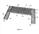
- Figures 2 and 3 are shown with transparent shield components to reveal the circuitry within them.
- a first embodiment of the invention comprises an ATM having a PIN pad 10 set into the ATM fascia 12.
- a PIN shield 14 is secured to the fascia 12 around the PIN pad 10 on three sides.
- the PIN shield 14 comprises:
- the PIN shield 14 may be formed: (a) of individual components 14a, 14b, 14c with the base member 14a secured on the fascia 12 and the flap 14c and side panels 14b secured on the base member, or (b) with one or more of the flap and side panels formed integrally with the base member, or (c) with the entire shield formed integrally as a single physical component.
- the side panels 14b are individual components secured to the U-shaped base member 14a by out-turned flanges 14d ( Figure 2 ) which are fitted to the base member in register with the opposite side arms 14e thereof ( Figure 3 ), while the flap 14c is formed integrally with the rear 14f of the base member 14a.
- the base member 14a is glued and/or screwed to the fascia 12 and the components 14b and 14c, when formed as separate components, are glued or screwed to the base member.
- the shield components 14a, 14b and 14c are typically moulded from a hard electrically insulating plastics material, whether the shield is formed as separate components or as a single physical piece. When fitted, the PIN shield 14 restricts a full view of the PIN pad 10 to a person located directly in front of the PIN pad, so that a person off to one side, or looking over the person's shoulder, obtains only a partial view of the PIN pad, if any.
- a conductive wire mesh 16 which in the embodiment is made of 40AWG Nichrome wire, is embedded in each of the base member 14a, side panels 14b and flap 14c.
- Figure 2 shows the portion 16a of the mesh which is embedded in the right hand side panel 14b, the left hand side panel being a mirror image of the right hand panel, and
- Figure 3 shows the portion 16b of the mesh which is embedded in the base member 14a and integral flap 14c.
- the mesh 16a comprises a single wire extending in the body of the panel continuously between two flat, 2.5mm diameter, circular metal contacts 17 exposed substantially flush with the bottom surface of the flange 14d at the rear of the side panel.
- the mesh 16b comprises a single wire connected across respective pins 19 of a two pin connector, the wire being interrupted by respective pairs of flat, 2.5mm diameter, circular metal contacts 18a, 18b which are exposed substantially flush with the top surface of the base member side arms 14e.
- the mesh portions 16a, 16b (right hand side) and 16b (left hand side) are connected in series between the contact pins 19 to form a continuous electrical conductor, comprising primarily the wire mesh 16 but locally by the contacts 17, 18a and 18b, extending from one contact pin 19 to the other contact pin 19 of the two pin connector.
- the contact pins 19 therefore constitute input and output terminals for the mesh 16 as a whole.
- the two-pin connector is of the low profile clip type and is fitted into a recess 20 in the bottom surface of the base member 14a.
- the connector is positioned horizontally in the PIN shield so that when a cable 22, Figure 5 , for connecting the wire mesh 16 to a microcontroller is attached, as will be described, the combination of the connector and its socket do not protrude beyond the bottom of the PIN shield.
- Physical impacts on the PIN shield components are generally more likely to be incident on the components in the direction perpendicular to their largest face. Specifically, impacts on the flap 14c of the PIN shield 14 are more likely to be from above and impacts on the side panels 14b are more likely to be from the side.
- the mesh wire 16 is therefore threaded throughout the shield components in a regularly spaced set of horizontal lines, approximately 2 to 5mm apart. Horizontal in this sense means parallel to the longest available axis of the component.
- a microcontroller (not shown), based on an ATMEL ATMega328P, is mounted within the body of the ATM below the fascia.
- Miscellaneous supporting circuitry for the microcontroller includes:
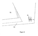
- the connector pins 19 ( Figure 4 ) are connected to the microcontroller by a cable 22 passing through a hole 24 drilled in the fascia 12.
- the wire mesh 16, comprising the series connected portions 16a, 16b and 16b, is configured as one resistor in a voltage divider, along with a second resistor (not shown) having a fixed resistance.
- the resistance of the second resistor is selected to be low relative to the resistance of the mesh 16. Therefore, in the voltage divider, the majority of the voltage will be dropped across the wire mesh.
- One of the microcontroller analog input pins is connected at the point between the two resistors (the wire mesh and the fixed value resistor respectively) and the voltage dropped across the wire mesh is monitored.
- the monitored voltage changes to a value which corresponds to the resistance of the mesh falling outside a predetermined range, due for example to a fracture of the mesh 16 indicating a possible attack on the PIN shield, an error condition is raised and an information LED is illuminated. Other alert actions, as described below are also invoked. The error status is maintained until the microcontroller is reset.
- each wire mesh portion 16a, 16b, 16b is connected to a separate input-output pin pair on the microcontroller.
- a random bit pattern is generated and transmitted on the respective output pin of the microcontroller.
- the bit pattern is then read, byte by byte, on the corresponding input pin.
- the received bit pattern is compared to the transmitted bit pattern. If the patterns do not match, an error condition is raised and an information LED is illuminated. Other alert actions, as described below, are also invoked. The error status is maintained until the microcontroller is reset.
- This implementation can modified by attaching all mesh portions 16a, 16b, 16b to a single microcontroller output pin, with separate input pins per mesh portion. The same bit pattern will then be received on all input pins.
- Alerts can be generated in two ways; either by directly reporting an alert status through the ATM PC core or by indirectly creating an error condition that will be detected by the ATM PC core.
- Direct reporting can be achieved by connecting the microcontroller via USB to the ATM PC core.
- a message is sent over the USB port.
- the microcontroller can be configured to repeat the transmission of the alert message at periodic time intervals or to repeat the transmission of the alert message a specific number of times.
- a USB driver is installed on the PC Core to receive the data transmitted by the microcontroller and convert this into an alert to be reported centrally (via Base24, SNMP or other mechanism).
- Indirect reporting can be achieved by disconnecting the power from another component within the ATM, for example, by disconnecting the power from the card reader or the PIN pad. This will cause an error to be generated by the PC core.
- the electrical continuation of the respective wire mesh portions from one shield portion to the other is made by terminating the wire mesh of one shield portion in two flat, 2.5mm diameter, circular metal contacts. Two similar contacts on the second shield portion are positioned so as to come into contact with the contacts on the first shield portion. When the two mesh portions are connected together the continuity of the wire mesh as between those two shield portions loop will be complete.
- two pieces of the PIN shield may move relative to each other, such as, for example, the "flap" may move relative to the base of the PIN shield. In such cases, an electrical connection between the two components is required.
- the coupling between the mesh and microcontroller is a direct resistive connection
- the coupling is inductive or capacitive, avoiding the need for the cable 22 to pass through the fascia and so for a hole to be formed in the fascia.
- a first comprises affixing a first set of electrodes 30 for a plurality capacitors to the underside of the fascia 12 and then forming a second set of electrodes (not shown) within each of the base members 14a and the flap 14c juxtaposed a respective one of the first set of electrodes.
- Each first set of electrodes 30 comprises an aluminium plate, approximately 2cm square and 1mm thick and surrounded by a non-conductive layer (and similarly for the second set of electrodes).
- the second set of electrodes can be interconnected with a pair of resistive meshes as in the first embodiment, so providing a pair of RC networks between a set of 3 leads 32 connecting the electrodes 30 to a microcontroller.
- the microcontroller can now measure either: the capacitance of each of the RC networks; or the time constant of the RC networks; or the resistance of the RC networks, once for calibration purposes and subsequently for monitoring purposes to determine if the shield has been removed or tampered with.
- the electrodes 30 can be used as one electrode of an open circuited arrangement where the shield does not incorporate discrete components interconnecting the electrodes 30.
- the shield may however be formed of electrically conducting material which affects the electrical characteristics of the exhibited at the electrodes 30.
- each of the electrodes 30 are connected back to the microcontroller via a number of resistors (not shown) to provide a pair of RC networks between three pins of the microcontroller, so allowing the microcontroller to measure and monitor the capacitance of the RC networks and to determine if the shield has been removed or tampered with as follows:
- Readings of the capacitance are then taken periodically, with a configured delay between each measurement (default 30 seconds).
- the difference between the reading and the baseline capacitance value is calculated and a rolling average of a configurable number of readings (default 5) is calculated.
- a status LED is illuminated to indicate that the device is now ready and able to detect deviations from the baseline.
- an error counter is incremented. If the average remains outside the tolerance window for a configured number of consecutive readings (default 10) then an error condition is raised and an information LED is illuminated. Other alert actions, as described in relation to the first embodiment, may also be invoked. The error status is maintained until the microcontroller is reset.
- Alert generation, direct reporting and indirect reporting are as described for the first embodiment.
Landscapes
- Business, Economics & Management (AREA)
- Accounting & Taxation (AREA)
- Physics & Mathematics (AREA)
- General Physics & Mathematics (AREA)
- Finance (AREA)
- Alarm Systems (AREA)
Priority Applications (1)
| Application Number | Priority Date | Filing Date | Title |
|---|---|---|---|
| EP15180144.6A EP3128490A1 (fr) | 2015-08-07 | 2015-08-07 | Protection de sécurité pour un clavier de saisie de données |
Applications Claiming Priority (1)
| Application Number | Priority Date | Filing Date | Title |
|---|---|---|---|
| EP15180144.6A EP3128490A1 (fr) | 2015-08-07 | 2015-08-07 | Protection de sécurité pour un clavier de saisie de données |
Publications (1)
| Publication Number | Publication Date |
|---|---|
| EP3128490A1 true EP3128490A1 (fr) | 2017-02-08 |
Family
ID=53800862
Family Applications (1)
| Application Number | Title | Priority Date | Filing Date |
|---|---|---|---|
| EP15180144.6A Withdrawn EP3128490A1 (fr) | 2015-08-07 | 2015-08-07 | Protection de sécurité pour un clavier de saisie de données |
Country Status (1)
| Country | Link |
|---|---|
| EP (1) | EP3128490A1 (fr) |
Cited By (1)
| Publication number | Priority date | Publication date | Assignee | Title |
|---|---|---|---|---|
| CN112585749A (zh) * | 2018-09-03 | 2021-03-30 | 安普林荷兰有限公司 | Rf返回电流损耗降低的功率放大器 |
Citations (11)
| Publication number | Priority date | Publication date | Assignee | Title |
|---|---|---|---|---|
| EP0622719A1 (fr) * | 1993-04-28 | 1994-11-02 | Siemens Nixdorf Informationssysteme AG | Dispositif de protection pour des éléments de circuit et/ou des données dans un appareil électrotechnique |
| DE19600769A1 (de) * | 1996-01-11 | 1997-07-17 | Ibm | Sicherheitsmodul mit einteiliger Sicherheitsfolie |
| DE29722653U1 (de) * | 1997-12-22 | 1999-01-28 | Siemens Ag | Manipulationsgeschütztes elektrisches Gerät |
| EP1873680A1 (fr) * | 2006-06-23 | 2008-01-02 | ddm hopt + schuler GmbH & Co. KG. | Lecteur de carte protégé contre la manipulation |
| US7337955B1 (en) * | 2005-12-20 | 2008-03-04 | Diebold Self-Service Systems Division Of Diebold, Incorporated | Cash dispensing automated banking machine system and method |
| DE102009044794A1 (de) * | 2009-12-07 | 2011-06-09 | Wincor Nixdorf International Gmbh | Sichtschutzelement eines Selbstbedienungsgerätes |
| WO2011070355A1 (fr) * | 2009-12-08 | 2011-06-16 | Alistair Taverner | Protection pour clavier |
| EP2431901A1 (fr) * | 2010-09-15 | 2012-03-21 | Compagnie Industrielle et Financière d'Ingénierie "Ingenico" | Dispositif de protection, procédé et produit programme d'ordinateur correspondant |
| EP2431899A1 (fr) * | 2010-09-15 | 2012-03-21 | Compagnie Industrielle et Financière d'Ingénierie "Ingenico" | Dispositif de protection, procédé et produit programme d'ordonateur correspondant |
| US20130069784A1 (en) * | 2011-09-15 | 2013-03-21 | Oki Electric Industry Co., Ltd. | Automated transaction apparatus |
| EP2793202A1 (fr) * | 2013-04-16 | 2014-10-22 | Wincor Nixdorf International GmbH | Appareil de libre-service doté d'un élément de protection optique |
-
2015
- 2015-08-07 EP EP15180144.6A patent/EP3128490A1/fr not_active Withdrawn
Patent Citations (11)
| Publication number | Priority date | Publication date | Assignee | Title |
|---|---|---|---|---|
| EP0622719A1 (fr) * | 1993-04-28 | 1994-11-02 | Siemens Nixdorf Informationssysteme AG | Dispositif de protection pour des éléments de circuit et/ou des données dans un appareil électrotechnique |
| DE19600769A1 (de) * | 1996-01-11 | 1997-07-17 | Ibm | Sicherheitsmodul mit einteiliger Sicherheitsfolie |
| DE29722653U1 (de) * | 1997-12-22 | 1999-01-28 | Siemens Ag | Manipulationsgeschütztes elektrisches Gerät |
| US7337955B1 (en) * | 2005-12-20 | 2008-03-04 | Diebold Self-Service Systems Division Of Diebold, Incorporated | Cash dispensing automated banking machine system and method |
| EP1873680A1 (fr) * | 2006-06-23 | 2008-01-02 | ddm hopt + schuler GmbH & Co. KG. | Lecteur de carte protégé contre la manipulation |
| DE102009044794A1 (de) * | 2009-12-07 | 2011-06-09 | Wincor Nixdorf International Gmbh | Sichtschutzelement eines Selbstbedienungsgerätes |
| WO2011070355A1 (fr) * | 2009-12-08 | 2011-06-16 | Alistair Taverner | Protection pour clavier |
| EP2431901A1 (fr) * | 2010-09-15 | 2012-03-21 | Compagnie Industrielle et Financière d'Ingénierie "Ingenico" | Dispositif de protection, procédé et produit programme d'ordinateur correspondant |
| EP2431899A1 (fr) * | 2010-09-15 | 2012-03-21 | Compagnie Industrielle et Financière d'Ingénierie "Ingenico" | Dispositif de protection, procédé et produit programme d'ordonateur correspondant |
| US20130069784A1 (en) * | 2011-09-15 | 2013-03-21 | Oki Electric Industry Co., Ltd. | Automated transaction apparatus |
| EP2793202A1 (fr) * | 2013-04-16 | 2014-10-22 | Wincor Nixdorf International GmbH | Appareil de libre-service doté d'un élément de protection optique |
Cited By (2)
| Publication number | Priority date | Publication date | Assignee | Title |
|---|---|---|---|---|
| CN112585749A (zh) * | 2018-09-03 | 2021-03-30 | 安普林荷兰有限公司 | Rf返回电流损耗降低的功率放大器 |
| CN112585749B (zh) * | 2018-09-03 | 2021-10-26 | 安普林荷兰有限公司 | Rf返回电流损耗降低的功率放大器 |
Similar Documents
| Publication | Publication Date | Title |
|---|---|---|
| US7988054B2 (en) | Secure card reader | |
| CA2638449C (fr) | Appareil de detection de fraudes pour compteurs electriques | |
| US7636050B2 (en) | Systems and methods for detecting a patch cord end connection | |
| US6476729B1 (en) | Power monitoring module with display unit for electrical power source device | |
| US5034723A (en) | Security cable and system for protecting electronic equipment | |
| US20080272878A1 (en) | Circuit breaking link status detection and reporting circuit | |
| US5274324A (en) | Hot line mountable hotline indicator having liquid crystal display with resettable memory function | |
| US20080116906A1 (en) | Apparatus and method for metering contact integrity | |
| WO2005086546A2 (fr) | Lecteur de cartes securise | |
| US20100268053A1 (en) | Method and Device for Detecting USB Cable Connection | |
| US9269241B2 (en) | Tamper-resistant security device | |
| US10901037B2 (en) | Method and apparatus for monitoring status of relay | |
| CA3005172A1 (fr) | Detecteur de violation de lecteur de carte | |
| US9830788B1 (en) | Anti-theft device for monitoring a universal serial bus type C connector | |
| WO2019073224A1 (fr) | Prise de courant | |
| WO2015057504A1 (fr) | Appareil et procédés de surveillance des interconnexions électriques à l'aide de dispositifs à rfid | |
| US6433982B1 (en) | Connection verifying trip unit | |
| WO2013118257A1 (fr) | Wattmètre électronique | |
| CN104698334B (zh) | 集成电路及判断集成电路的接脚连接状况的方法 | |
| KR102038711B1 (ko) | 패치패널 및 이를 구비하는 패치코드 관리 시스템 | |
| JP2019193542A (ja) | 異常検知システム及び異常検知方法 | |
| US20150054536A1 (en) | Pin Verification Device And Method | |
| US20160181739A1 (en) | Gfci with cycle counter | |
| US10074250B2 (en) | Anti-theft device for monitoring connection between a male plug and a female receptacle | |
| CN213987231U (zh) | 一种二线tmr传感器、pcb板及其控制电路 |
Legal Events
| Date | Code | Title | Description |
|---|---|---|---|
| PUAI | Public reference made under article 153(3) epc to a published international application that has entered the european phase |
Free format text: ORIGINAL CODE: 0009012 |
|
| AK | Designated contracting states |
Kind code of ref document: A1 Designated state(s): AL AT BE BG CH CY CZ DE DK EE ES FI FR GB GR HR HU IE IS IT LI LT LU LV MC MK MT NL NO PL PT RO RS SE SI SK SM TR |
|
| AX | Request for extension of the european patent |
Extension state: BA ME |
|
| STAA | Information on the status of an ep patent application or granted ep patent |
Free format text: STATUS: THE APPLICATION IS DEEMED TO BE WITHDRAWN |
|
| 18D | Application deemed to be withdrawn |
Effective date: 20170809 |