EP3128558B1 - Transistor à couche mince et son procédé de fabrication et dispositif d'affichage - Google Patents
Transistor à couche mince et son procédé de fabrication et dispositif d'affichage Download PDFInfo
- Publication number
- EP3128558B1 EP3128558B1 EP15850214.6A EP15850214A EP3128558B1 EP 3128558 B1 EP3128558 B1 EP 3128558B1 EP 15850214 A EP15850214 A EP 15850214A EP 3128558 B1 EP3128558 B1 EP 3128558B1
- Authority
- EP
- European Patent Office
- Prior art keywords
- layer
- active layer
- thin film
- ohmic contact
- film transistor
- Prior art date
- Legal status (The legal status is an assumption and is not a legal conclusion. Google has not performed a legal analysis and makes no representation as to the accuracy of the status listed.)
- Active
Links
Images

Classifications
-
- H—ELECTRICITY
- H10—SEMICONDUCTOR DEVICES; ELECTRIC SOLID-STATE DEVICES NOT OTHERWISE PROVIDED FOR
- H10D—INORGANIC ELECTRIC SEMICONDUCTOR DEVICES
- H10D30/00—Field-effect transistors [FET]
- H10D30/01—Manufacture or treatment
- H10D30/021—Manufacture or treatment of FETs having insulated gates [IGFET]
- H10D30/031—Manufacture or treatment of FETs having insulated gates [IGFET] of thin-film transistors [TFT]
-
- H—ELECTRICITY
- H10—SEMICONDUCTOR DEVICES; ELECTRIC SOLID-STATE DEVICES NOT OTHERWISE PROVIDED FOR
- H10D—INORGANIC ELECTRIC SEMICONDUCTOR DEVICES
- H10D30/00—Field-effect transistors [FET]
- H10D30/60—Insulated-gate field-effect transistors [IGFET]
- H10D30/67—Thin-film transistors [TFT]
-
- H—ELECTRICITY
- H10—SEMICONDUCTOR DEVICES; ELECTRIC SOLID-STATE DEVICES NOT OTHERWISE PROVIDED FOR
- H10D—INORGANIC ELECTRIC SEMICONDUCTOR DEVICES
- H10D30/00—Field-effect transistors [FET]
- H10D30/60—Insulated-gate field-effect transistors [IGFET]
- H10D30/67—Thin-film transistors [TFT]
- H10D30/6704—Thin-film transistors [TFT] having supplementary regions or layers in the thin films or in the insulated bulk substrates for controlling properties of the device
- H10D30/6713—Thin-film transistors [TFT] having supplementary regions or layers in the thin films or in the insulated bulk substrates for controlling properties of the device characterised by the properties of the source or drain regions, e.g. compositions or sectional shapes
-
- H—ELECTRICITY
- H10—SEMICONDUCTOR DEVICES; ELECTRIC SOLID-STATE DEVICES NOT OTHERWISE PROVIDED FOR
- H10D—INORGANIC ELECTRIC SEMICONDUCTOR DEVICES
- H10D30/00—Field-effect transistors [FET]
- H10D30/60—Insulated-gate field-effect transistors [IGFET]
- H10D30/67—Thin-film transistors [TFT]
- H10D30/674—Thin-film transistors [TFT] characterised by the active materials
- H10D30/6755—Oxide semiconductors, e.g. zinc oxide, copper aluminium oxide or cadmium stannate
-
- H—ELECTRICITY
- H10—SEMICONDUCTOR DEVICES; ELECTRIC SOLID-STATE DEVICES NOT OTHERWISE PROVIDED FOR
- H10D—INORGANIC ELECTRIC SEMICONDUCTOR DEVICES
- H10D30/00—Field-effect transistors [FET]
- H10D30/60—Insulated-gate field-effect transistors [IGFET]
- H10D30/67—Thin-film transistors [TFT]
- H10D30/6757—Thin-film transistors [TFT] characterised by the structure of the channel, e.g. transverse or longitudinal shape or doping profile
-
- H—ELECTRICITY
- H10—SEMICONDUCTOR DEVICES; ELECTRIC SOLID-STATE DEVICES NOT OTHERWISE PROVIDED FOR
- H10D—INORGANIC ELECTRIC SEMICONDUCTOR DEVICES
- H10D62/00—Semiconductor bodies, or regions thereof, of devices having potential barriers
- H10D62/80—Semiconductor bodies, or regions thereof, of devices having potential barriers characterised by the materials
-
- H—ELECTRICITY
- H10—SEMICONDUCTOR DEVICES; ELECTRIC SOLID-STATE DEVICES NOT OTHERWISE PROVIDED FOR
- H10D—INORGANIC ELECTRIC SEMICONDUCTOR DEVICES
- H10D64/00—Electrodes of devices having potential barriers
- H10D64/60—Electrodes characterised by their materials
- H10D64/62—Electrodes ohmically coupled to a semiconductor
-
- H—ELECTRICITY
- H10—SEMICONDUCTOR DEVICES; ELECTRIC SOLID-STATE DEVICES NOT OTHERWISE PROVIDED FOR
- H10D—INORGANIC ELECTRIC SEMICONDUCTOR DEVICES
- H10D86/00—Integrated devices formed in or on insulating or conducting substrates, e.g. formed in silicon-on-insulator [SOI] substrates or on stainless steel or glass substrates
- H10D86/40—Integrated devices formed in or on insulating or conducting substrates, e.g. formed in silicon-on-insulator [SOI] substrates or on stainless steel or glass substrates characterised by multiple TFTs
- H10D86/421—Integrated devices formed in or on insulating or conducting substrates, e.g. formed in silicon-on-insulator [SOI] substrates or on stainless steel or glass substrates characterised by multiple TFTs having a particular composition, shape or crystalline structure of the active layer
- H10D86/423—Integrated devices formed in or on insulating or conducting substrates, e.g. formed in silicon-on-insulator [SOI] substrates or on stainless steel or glass substrates characterised by multiple TFTs having a particular composition, shape or crystalline structure of the active layer comprising semiconductor materials not belonging to the Group IV, e.g. InGaZnO
-
- H—ELECTRICITY
- H10—SEMICONDUCTOR DEVICES; ELECTRIC SOLID-STATE DEVICES NOT OTHERWISE PROVIDED FOR
- H10D—INORGANIC ELECTRIC SEMICONDUCTOR DEVICES
- H10D86/00—Integrated devices formed in or on insulating or conducting substrates, e.g. formed in silicon-on-insulator [SOI] substrates or on stainless steel or glass substrates
- H10D86/40—Integrated devices formed in or on insulating or conducting substrates, e.g. formed in silicon-on-insulator [SOI] substrates or on stainless steel or glass substrates characterised by multiple TFTs
- H10D86/60—Integrated devices formed in or on insulating or conducting substrates, e.g. formed in silicon-on-insulator [SOI] substrates or on stainless steel or glass substrates characterised by multiple TFTs wherein the TFTs are in active matrices
-
- H—ELECTRICITY
- H10—SEMICONDUCTOR DEVICES; ELECTRIC SOLID-STATE DEVICES NOT OTHERWISE PROVIDED FOR
- H10D—INORGANIC ELECTRIC SEMICONDUCTOR DEVICES
- H10D99/00—Subject matter not provided for in other groups of this subclass
Definitions
- Embodiments of the present invention relate to field of display technique, particularly to a thin film transistor and a method for manufacturing the same and a display device.
- a semiconductor active layer is made of metallic oxide semiconductor material, which, however, can not adapt well to various manufacturing conditions of different manufacturing processes and problems such as low electron mobility, poor ohminc contact property will occur. Meanwhile, the semiconductor active layer may be damaged, even losing a semiconductor property due to influences of manufacturing environments, plasma treatments, pollution treatments and the like in different manufacturing processes.
- US 2014/159035 A1 discloses a thin film transistor and a method of making it.
- the transistor may include a gate electrode, a gate insulating layer, and a channel layer stacked on each other; and a source electrode and a drain electrode contacting first and second regions of the channel layer, respectively.
- the channel layer may include oxynitride.
- Embodiments of the present invention provide a thin film transistor and a method for manufacturing the same and a display device, which can solve the problem of poor ohmic contact property between an active layer of a zinc oxynitride material and a source/drain electrode in an existing thin film transistor, improving the ohmic contact property of the active layer with the source and drain electrodes. Meanwhile, image display effect of a display is improved.
- a thin film transistor in accordance with claim 1 comprising an active layer, a source electrode, a drain electrode, and an ohmic contact layer disposed between the active layer and the source electrode and/or between the active layer and the drain electrode to improve an ohmic contact property between the active layer and the source electrode and/or between the active layer and the drain electrode, wherein the active layer is made of zinc oxynitride, and the ohmic contact layer is made of zinc nitride, wherein the thin film transistor further comprises a gate insulation layer and a gate electrode, wherein the active layer is disposed on a substrate; the gate insulation layer is disposed on the active layer to partially expose the active layer; the gate electrode is disposed on the gate insulation layer at a position corresponding to the gate insulation layer; the ohmic contact layer is disposed on the exposed active layer; and the source electrode and the drain electrode are disposed on the ohmic contact layer.
- the thin film transistor further comprises a finishing layer, wherein the finishing layer is disposed on the ohmic contact layer and provided with via holes therein at positions corresponding to the source electrode and the drain electrode; and the finishing layer is made of metallic or nonmetallic nitride.
- the active layer has a thickness of 200-1500 ⁇ .
- each of the source electrode and the drain electrode has a thickness of 50-100 ⁇ .
- the ohmic contact layer has a thickness less than 50 ⁇ .
- the finishing layer has a thickness of 30-300 ⁇ .
- the forming an ohmic contact layer between the active layer and the source electrode and/or between the active layer and the drain electrode comprises: forming a nitride thin film between the active layer and the source and drain electrodes by using a metallic or nonmetallic nitride material so that a nitride in the nitride thin film reacts with the zinc oxynitride in the active layer to form the ohmic contact layer.
- the forming an ohmic contact layer between the active layer and the source electrode and/or between the active layer and the drain electrode comprises: forming the ohmic contact layer between the active layer and the source electrode and/or between the active and the drain electrode directly by using a zinc nitride material.
- the method further comprises forming the gate insulation layer and the gate electrode through a single pattering process.
- a display device comprising the thin film transistor in any one of the above embodiments of the one aspect of the present invention.
- the ohmic contact layer made of the zinc nitride is formed between the active layer and the source electrode and/or between the active layer and the drain electrode. Since the zinc nitride material has a good ohmic contact property, the ohmic contact layer made of zinc nitride will provide a good ohmic contact property between the source and drain electrodes and the active layer. Therefore, it is possible to solve the problem of poor ohmic contact effect between the active layer of zinc oxynitride and the source and drain electrodes in the prior art, thereby improving the ohmic contact property between the active layer and the source and drain electrodes in the existing thin film transistor. Thus, the image display effect of a display can be improved.
- the gate electrode compared to the prior art in which the gate electrode must have a larger area than that of the active layer in order to ensure the performance of the thin film transistor, in embodiments of the present invention, since the ohmic contact layer is additionally provided, an area of the gate electrode is greatly reduced compared to that of the prior art, which can in turn effectively reduce an area of the active layer such that a parasitic capacitance between the source and drain electrodes and the gate electrode is reduced. Therefore, it is possible to further improve image display effect of a display.
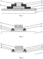
- An embodiment of the present invention provides a thin film transistor as shown in Figure 1 .
- the thin film transistor comprises a substrate 1, a gate electrode 2, a gate insulation layer 3, an active layer 4, a source electrode 5, a drain electrode 6 and an ohmic contact layer 7.
- the ohmic contact layer 7 is disposed between the active layer 4 and the source electrode 5 and between the active layer 4 and the drain electrode 6.
- the ohmic contact layer 7 is made of zinc nitride.
- the ohmic contact layer in this embodiment is made of zinc nitride.
- the zinc nitride material has a good ohmic contact property.
- the ohmic contact layer is located between the active layer and the source and drain electrodes.
- the zinc nitride can generate large amounts of charges and has a good electrical conductivity. Therefore, the ohmic contact property between the active layer and the source and drain electrodes in the thin film transistor of the present embodiment is better than the ohmic contact property between the active layer and the source and drain electrodes in a structure in the prior art in which only the source and drain electrodes contact the active layer, so that there will not generate a relatively large signal delay in a display device having the thin film transistor, thereby avoiding a problem of poor image display quality.
- the substrate may include a glass substrate, a quartz substrate or the like.
- the gate electrode may be made of metal material and the like.
- the gate insulation layer may be made of silicon nitride, or it may also be made of silicon oxide, silicon oxynitride and the like.
- FIG. 2 is a schematic structural view of a thin film transistor according to another exemplary embodiment of the present invention.
- an active layer 4 of the thin film transistor is disposed on a substrate 1.
- a gate insulation layer 3 is disposed on the active layer 4 so that the active layer 4 is partially exposed.
- a gate electrode 2 is disposed on the gate insulation layer 3 at a position corresponding to the gate insulation layer 3.
- a source electrode 5 and a drain electrode 6 are disposed on an ohmic contact layer 7.
- the active layer 4 is made of zinc oxynitride and may have a thickness of 200-1500 ⁇ .
- Each of the source electrode 5 and the drain electrode 6 may have a thickness of 50-100 ⁇ .
- the ohmic contact layer may have a thickness less than 50 ⁇ .
- the ohmic contact layer 7 may be obtained by reaction of a metallic nitride or a nonmetallic nitride thin film formed between the active layer and the source and drain electrodes with the zinc oxide in the active layer.
- the active layer is disposed in contact with the substrate, and then the gate insulation layer and the gate electrode are sequentially formed; the ohmic contact layer is provided on the active layer, and then the source electrode and the drain electrode are provided on the ohmic contact layer. Since the ohmic contact layer is formed through the reaction of the zinc oxynitride in the active layer with the nitride thin film, a thickness of a film layer is not additionally increased.
- a width of a channel region of the thin film transistor is decreased, and an improved ohmic contact property between the active layer and the source and drain electrodes of the thin film transistor is ensured, which greatly reduces a size of the thin film transistor and saves manufacturing cost.
- a single patterning process is used to form the gate insulation layer and the gate electrode during manufacturing, thereby reducing manufacturing steps.
- FIG 3 is a schematic structural view of a thin film transistor according to another exemplary embodiment of the present invention.
- the thin film transistor further comprises a finishing layer 8.
- the finishing layer 8 is disposed on the ohmic contact layer 7 and provided with via holes therein at positions corresponding to the source electrode 5 and the drain electrode 6.
- the finishing layer 8 is made of metallic or nonmetallic nitride.
- the finishing layer is made of aluminum nitride.
- the finishing layer 8 may have a thickness of 30-300 ⁇ . Preferably, the finishing layer 8 has a thickness of 30-120 ⁇ .
- a layer of nitride thin film is formed on the gate electrode to cover the substrate, the gate electrode and the active layer when initially forming the finishing layer. Since the nitride thin film directly contacts the active layer, the metallic or nonmetallic nitride thin film forming the finishing layer will chemically react with the zinc oxynitride of the active layer to produce zinc nitride so as to form the ohmic contact layer. That is, the ohmic contact layer is formed at a position where the nitride thin film is in contact with the active layer.
- the ohmic contact layer may be formed at a position corresponding to the active layer by directly forming a layer of zinc nitride thin film on the gate electrode by magnetron sputtering and then patterning the nitride thin film with a mask plate after various patterning processes such as exposure, development, etching, peeling and the like.
- the ohmic contact layer made of the zinc nitride is formed between the active layer and the source electrode and the active layer and the drain electrode. Since the zinc nitride material has a good ohmic contact property, the ohmic contact layer made of zinc nitride will provide a good ohmic contact property between the source and drain electrodes and the active layer. Therefore, it is possible to solve the problem of poor ohmic contact effect between the active layer of zinc oxynitride and the source and drain electrodes, thereby improving the ohmic contact property between the active layer and the source and drain electrodes in the thin film transistor.
- the gate electrode has a larger area than that of the active layer to ensure the performance of the thin film transistor
- the ohmic contact layer is additionally provided, an area of the gate electrode is greatly reduced compared to that of the prior art, which can in turn effectively reduce an area of the active layer such that a parasitic capacitance between the source and drain electrodes and the gate electrode is reduced. Therefore, it is possible to improve image display effect of a display comprising the thin film transistor of the present disclosure.
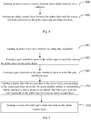
- the method comprises: S101: forming an active layer, a source electrode and a drain electrode on a substrate.
- a thin film of zinc oxynitride having a thickness of 200-1500 ⁇ on a substrate such as a glass substrate or a quartz substrate through a chemical vapor deposition process and then performing a single patterning process on the thin film of zinc oxynitride to form the active layer, and thereafter, depositing a layer of metal thin film on the active layer.
- the metal thin film is typically selected from a group consisting of molybdenum, aluminum, aluminum-nickel alloy, molybdenum tungsten alloy, chromium, copper or the combination thereof.
- the order of forming the active layer and the source and drain electrodes there is not any limitation to the order of forming the active layer and the source and drain electrodes. It is possible to firstly form the active layer and then form the source and drain electrodes. Alternatively, it is possible to firstly form the source and drain electrodes and then form the active layer.
- S102 forming an ohmic contact layer between the active layer and the source electrode and between the active layer and the drain electrode.
- the method comprises: S201: forming an active layer on a substrate by using zinc oxynitride.
- a thin film of zinc oxynitride having a thickness of 200-1500 ⁇ on a substrate such as a glass substrate or a quartz substrate through a chemical vapor deposition process and then perform a single patterning process on the thin film of zinc oxynitride to form the active layer. That is, after applying a photoresist layer, performing exposure, development and etching processes on the substrate to form the active layer by using a mask plate.
- steps S202 and S203 it is possible to deposit an insulation thin film on the active layer through a chemical vapor deposition process or a magnetron sputtering process.
- the insulation thin film is typically made of silicon nitride. It may also be made of silicon oxide, silicon oxynitride or the like.
- the metal thin film is typically formed by molybdenum, aluminum, aluminum-nickel alloy, molybdenum tungsten alloy, chromium, copper or the combination thereof.
- the insulation thin film and the metal thin film are processed to form the gate insulation layer on a predetermined region of the active layer for partially exposing the active layer and the gate electrode through a single patterning process such as exposure, development, etching, peeling and the like.
- S204 forming a nitride thin film at a position of the active layer corresponding to the source and drain electrodes by using metallic nitride or nonmetallic nitride material so that a nitride in the nitride thin film reacts with the zinc oxynitride in the active layer to form an ohmic contact layer.
- nitride thin film covering the substrate, the gate electrode and the active layer and having a thickness of 30-300 ⁇ on the gate electrode through a magnetron sputtering process. Then, the nitride thin film will react with the zinc oxynitride in the active layer to form a thin film of zinc nitride, i.e., the ohmic contact layer having a thickness less than 50 ⁇ on a predetermined region of the active layer.
- S205 forming a source electrode and a drain electrode on the ohmic contact layer.
- a metal thin film having a thickness of 50-100 ⁇ on the ohmic contact layer by the same process as that for forming the gate electrode, and then to form the source and drain electrodes on a predetermined region through a patterning process.
- the method comprises: S301: forming a gate electrode on a substrate.
- a layer of metal thin film on a substrate such as a glass substrate or a quartz substrate by a magnetron sputtering process.
- the metal thin film may typically formed by molybdenum, aluminum, aluminum-nickel alloy, molybdenum tungsten alloy, chromium, copper or the combination thereof.
- the gate insulation layer thin film is typically made of silicon nitride. It may also be made of silicon oxide, silicon oxynitride and the like.
- S304 forming an ohmic contact layer on the active layer at a position corresponding to the source electrode and drain electrode.
- a metallic or nonmetallic nitride thin film having a thickness of 30-300 ⁇ and covering an ohmic contact region of the active layer on the active layer through a patterning process.
- the thin film is made of aluminum nitride. Then, the nitride thin film reacts with the zinc oxynitride in the active layer to form a zinc nitride thin film, i.e., the ohmic contact layer having a thickness less than 50 ⁇ at a position of the active layer in contact with source and drain electrodes.
- a metal thin film similar to a gate electrode metal having a thickness of 50-100 ⁇ on the substrate by the same process as that for forming the gate electrode metal layer, and then to form the source and drain electrodes on a predetermined region through a patterning process.
- a display device comprising the thin film transistor as described in the above embodiments of the present invention.
- an ohmic contact layer is formed in the thin film transistor between the active layer and the source electrode and between the active layer and the drain electrode by using zinc nitride material. Since the zinc nitride material has a good ohmic contact property, the ohmic contact layer made of the zinc nitride will provide a good ohmic contact property between the source and drain electrodes and the active layer. Therefore, it is possible to solve the problem of poor ohmic contact effect between the active layer of zinc oxynitride and the source and drain electrodes in the prior art, thereby improving the ohmic contact property between the active layer and the source and drain electrodes.
- the display device having the thin film transistor as described above improves image display effect of a display.
Landscapes
- Thin Film Transistor (AREA)
- Electrodes Of Semiconductors (AREA)
Claims (10)
- Transistor en couches minces comprenantune couche active (4) ;une électrode de source (5) ;une électrode de drain (6) ; etune couche de contact ohmique (7),la couche de contact ohmique (7) étant disposée entre la couche active (4) et l'électrode de source (5) et/ou entre la couche active (4) et l'électrode de drain (6) pour améliorer une propriété de contact ohmique entre la couche active (4) et l'électrode de source (5) et/ou entre la couche active (4) et l'électrode de drain (6), dans lequella couche active (4) est constituée d'oxynitrure de zinc ; etla couche de contact ohmique (7) est constituée de nitrure de zinc,et en ce que le transistor en couches minces comprend en outre une couche d'isolation de grille (3) et une électrode de grille (2), dans lequella couche active (4) est disposée sur un substrat (1) ;la couche d'isolation de grille (3) est disposée sur la couche active (4) pour exposer partiellement la couche active (4) ;l'électrode de grille (2) est disposée sur la couche d'isolation de grille (3) à une position correspondant à la couche d'isolation de grille (3) ;la couche de contact ohmique (7) est disposée sur la couche active exposée ; etl'électrode de source (5) et l'électrode de drain (6) sont disposées sur la couche de contact ohmique (7).
- Transistor en couches minces selon la revendication 1, comprenant en outre une couche de finition (8), dans lequella couche de finition (8) est disposée sur la couche de contact ohmique (7) et pourvue à l'intérieur de trous d'interconnexion à des positions correspondant à l'électrode de source (5) et l'électrode de drain (6) ; etla couche de finition (8) est constituée de nitrure métallique ou non métallique.
- Transistor en couches minces selon la revendication 1, dans lequel la couche active (4) a une épaisseur de 200-1500 Å.
- Transistor en couches minces selon la revendication 1, dans lequel l'électrode de source (5) et l'électrode de drain (6) ont chacune une épaisseur de 50-100 Å.
- Transistor en couches minces selon la revendication 1, dans lequel la couche de contact ohmique (7) a une épaisseur inférieure à 50 Å.
- Transistor en couches minces selon la revendication 3, dans lequel la couche de finition (8) a une épaisseur de 30-300 Å.
- Procédé de fabrication d'un transistor en couches minces comprenant une couche active (4), une électrode de source (5) et une électrode de drain (6), le procédé comprenant :la formation d'une couche de contact ohmique (7) entre la couche active (4) et l'électrode de source (5) et/ou entre la couche active (4) et l'électrode de drain (6), dans lequella couche active (4) est constituée d'oxynitrure de zinc, et la couche de contact ohmique (7) est constituée de nitrure de zinc,la formation d'une couche de contact ohmique (7) entre la couche active (4) et l'électrode de source (5) et/ou entre la couche active (4) et l'électrode de drain (6) comprend :la formation d'une couche mince de nitrure entre la couche active (4) et l'électrode de source (5) et/ou entre la couche active (4) et l'électrode de drain (6) au moyen d'un matériau en nitrure métallique ou non métallique de telle sorte qu'un nitrure dans la couche mince de nitrure réagisse avec l'oxynitrure de zinc dans la couche active (4) pour former la couche de contact ohmique (7),le procédé comprenant en outre :la formation de la couche active (4) sur un substrat (1) au moyen d'un matériau en oxynitrure de zinc ;la formation d'une couche d'isolation de grille (3) sur la couche active (4) pour exposer partiellement la couche active (4) ;la formation d'une électrode de grille (2) sur la couche d'isolation de grille (3) pour recouvrir la couche d'isolation de grille (3) ;la formation de la couche de contact ohmique (7) sur la couche active exposée ; etla formation de l'électrode de source (5) et de l'électrode de drain (6) sur la couche de contact ohmique (7) .
- Procédé selon la revendication 7, dans lequel la formation d'une couche de contact ohmique (7) entre la couche active (4) et l'électrode de source (5) et/ou entre la couche active (4) et l'électrode de drain (6) comprend :
la formation de la couche de contact ohmique (7) entre la couche active (4) et l'électrode de source (5) et/ou entre la couche active (4) et l'électrode de drain (6) directement au moyen d'un matériau en nitrure de zinc. - Procédé selon la revendication 7, comprenant en outre
la formation de la couche d'isolation de grille (3) et de l'électrode de grille (2) par une seule opération de modelage. - Dispositif d'affichage comprenant le transistor en couches minces selon l'une quelconque des revendications 1 à 6.
Applications Claiming Priority (2)
| Application Number | Priority Date | Filing Date | Title |
|---|---|---|---|
| CN201410546475.0A CN104362180B (zh) | 2014-10-15 | 2014-10-15 | 一种薄膜晶体管及其制作方法、显示基板和显示装置 |
| PCT/CN2015/073358 WO2016058312A1 (fr) | 2014-10-15 | 2015-02-27 | Transistor à couche mince et son procédé de fabrication, substrat d'affichage et dispositif d'affichage |
Publications (3)
| Publication Number | Publication Date |
|---|---|
| EP3128558A1 EP3128558A1 (fr) | 2017-02-08 |
| EP3128558A4 EP3128558A4 (fr) | 2017-11-22 |
| EP3128558B1 true EP3128558B1 (fr) | 2021-11-24 |
Family
ID=52529424
Family Applications (1)
| Application Number | Title | Priority Date | Filing Date |
|---|---|---|---|
| EP15850214.6A Active EP3128558B1 (fr) | 2014-10-15 | 2015-02-27 | Transistor à couche mince et son procédé de fabrication et dispositif d'affichage |
Country Status (4)
| Country | Link |
|---|---|
| US (1) | US9761725B2 (fr) |
| EP (1) | EP3128558B1 (fr) |
| CN (1) | CN104362180B (fr) |
| WO (1) | WO2016058312A1 (fr) |
Families Citing this family (4)
| Publication number | Priority date | Publication date | Assignee | Title |
|---|---|---|---|---|
| CN104362180B (zh) | 2014-10-15 | 2017-02-22 | 京东方科技集团股份有限公司 | 一种薄膜晶体管及其制作方法、显示基板和显示装置 |
| WO2017045135A1 (fr) * | 2015-09-15 | 2017-03-23 | Boe Technology Group Co., Ltd. | Substrat matriciel de transistor à couches minces et son procédé de fabrication, et dispositif d'affichage |
| CN106898654B (zh) * | 2017-03-07 | 2020-02-18 | 京东方科技集团股份有限公司 | 一种薄膜晶体管及其制备方法、阵列基板、显示装置 |
| JP7356815B2 (ja) * | 2019-05-14 | 2023-10-05 | トライベイル テクノロジーズ, エルエルシー | 薄膜トランジスタ基板及び表示装置 |
Family Cites Families (15)
| Publication number | Priority date | Publication date | Assignee | Title |
|---|---|---|---|---|
| US7071045B2 (en) * | 2004-05-06 | 2006-07-04 | Chunghwa Picture Tubes, Ltd. | Process of manufacturing thin film transistor |
| KR20090124527A (ko) * | 2008-05-30 | 2009-12-03 | 삼성모바일디스플레이주식회사 | 박막 트랜지스터, 그의 제조 방법 및 박막 트랜지스터를구비하는 평판 표시 장치 |
| EP2184783B1 (fr) * | 2008-11-07 | 2012-10-03 | Semiconductor Energy Laboratory Co, Ltd. | Dispositif semi-conducteur et son procédé de fabrication |
| CN101414564B (zh) * | 2008-11-24 | 2010-07-14 | 上海广电光电子有限公司 | 低温多晶硅薄膜晶体管的制造方法 |
| KR101281463B1 (ko) * | 2010-07-06 | 2013-07-03 | 엘지디스플레이 주식회사 | 박막 트랜지스터 기판 및 그를 이용한 액정표시장치 |
| TWI405335B (zh) * | 2010-09-13 | 2013-08-11 | Au Optronics Corp | 半導體結構及其製造方法 |
| KR101980195B1 (ko) * | 2012-05-16 | 2019-05-21 | 삼성전자주식회사 | 황 도핑 징크옥시 나이트라이드 채널층을 가진 트랜지스터 및 그 제조방법 |
| CN102890378B (zh) | 2012-09-17 | 2015-01-21 | 京东方科技集团股份有限公司 | 一种阵列基板及其制造方法 |
| KR101980196B1 (ko) * | 2012-12-10 | 2019-05-21 | 삼성전자주식회사 | 트랜지스터와 그 제조방법 및 트랜지스터를 포함하는 전자소자 |
| CN103199112B (zh) | 2013-03-20 | 2017-02-15 | 北京京东方光电科技有限公司 | 一种阵列基板及其制备方法和显示面板 |
| CN103219391B (zh) * | 2013-04-07 | 2016-03-02 | 京东方科技集团股份有限公司 | 一种薄膜晶体管及其制作方法、阵列基板和显示装置 |
| KR102147849B1 (ko) * | 2013-08-05 | 2020-08-25 | 삼성전자주식회사 | 박막 트랜지스터 및 그 제조방법 |
| KR20150025621A (ko) * | 2013-08-29 | 2015-03-11 | 삼성전자주식회사 | 트랜지스터와 그 제조방법 및 트랜지스터를 포함하는 전자소자 |
| CN103474356B (zh) * | 2013-09-17 | 2016-08-17 | 深圳丹邦投资集团有限公司 | 一种氮氧锌薄膜的制备方法 |
| CN104362180B (zh) | 2014-10-15 | 2017-02-22 | 京东方科技集团股份有限公司 | 一种薄膜晶体管及其制作方法、显示基板和显示装置 |
-
2014
- 2014-10-15 CN CN201410546475.0A patent/CN104362180B/zh active Active
-
2015
- 2015-02-27 EP EP15850214.6A patent/EP3128558B1/fr active Active
- 2015-02-27 US US15/307,362 patent/US9761725B2/en active Active
- 2015-02-27 WO PCT/CN2015/073358 patent/WO2016058312A1/fr not_active Ceased
Non-Patent Citations (1)
| Title |
|---|
| None * |
Also Published As
| Publication number | Publication date |
|---|---|
| CN104362180B (zh) | 2017-02-22 |
| CN104362180A (zh) | 2015-02-18 |
| WO2016058312A1 (fr) | 2016-04-21 |
| US20170047451A1 (en) | 2017-02-16 |
| EP3128558A1 (fr) | 2017-02-08 |
| EP3128558A4 (fr) | 2017-11-22 |
| US9761725B2 (en) | 2017-09-12 |
Similar Documents
| Publication | Publication Date | Title |
|---|---|---|
| US9099440B2 (en) | Manufacturing method of array substrate, array substrate and display | |
| US9508808B2 (en) | Manufacturing method of thin film transistor and manufacturing method of array substrate | |
| CN101770121B (zh) | Tft-lcd阵列基板及其制造方法 | |
| US20160254298A1 (en) | Array Substrate, Manufacturing Method Thereof, and Display Device | |
| US9704998B2 (en) | Thin film transistor and method of manufacturing the same, display substrate, and display apparatus | |
| US8199270B2 (en) | TFT-LCD array substrate and method of manufacturing the same | |
| US20160284741A1 (en) | Array substrate fabricating method | |
| US20150115258A1 (en) | Array substrate for liquid crystal display device and method of manufacturing the same | |
| EP3128558B1 (fr) | Transistor à couche mince et son procédé de fabrication et dispositif d'affichage | |
| US20160380105A1 (en) | Oxide thin film transistor and method for manufacturing the same, array substrate and method for manufacturing the same, and display device | |
| WO2016165517A1 (fr) | Substrat de réseau et son procédé de fabrication et panneau d'affichage | |
| US10593807B2 (en) | Array substrate and fabricating method thereof | |
| US10833107B2 (en) | Thin film transistor, manufacturing method therefor, array substrate and display device | |
| US10361261B2 (en) | Manufacturing method of TFT substrate, TFT substrate, and OLED display panel | |
| CN104377246A (zh) | 一种薄膜晶体管及其制作方法、阵列基板和显示装置 | |
| US9508762B2 (en) | Array substrate, method of manufacturing array substrate and display device | |
| US9881945B2 (en) | Methods of manufacturing thin film transistor and array substrate | |
| CN113782616A (zh) | 一种薄膜晶体管及其制备方法、阵列基板、显示装置 | |
| US11889721B2 (en) | Display substrate, manufacturing method thereof and display device | |
| WO2019127681A1 (fr) | Substrat de réseau et procédé de préparation | |
| CN107134497A (zh) | 薄膜晶体管及其制造方法、显示基板 | |
| US10497724B2 (en) | Manufacturing method of a thin film transistor and manufacturing method of an array substrate | |
| US9673228B2 (en) | Display panel | |
| WO2020000629A1 (fr) | Substrat matriciel et son procédé de fabrication ainsi que panneau d'affichage | |
| US10204942B1 (en) | Method for manufacturing top-gated thin film transistors |
Legal Events
| Date | Code | Title | Description |
|---|---|---|---|
| STAA | Information on the status of an ep patent application or granted ep patent |
Free format text: STATUS: THE INTERNATIONAL PUBLICATION HAS BEEN MADE |
|
| PUAI | Public reference made under article 153(3) epc to a published international application that has entered the european phase |
Free format text: ORIGINAL CODE: 0009012 |
|
| STAA | Information on the status of an ep patent application or granted ep patent |
Free format text: STATUS: REQUEST FOR EXAMINATION WAS MADE |
|
| 17P | Request for examination filed |
Effective date: 20161031 |
|
| AK | Designated contracting states |
Kind code of ref document: A1 Designated state(s): AL AT BE BG CH CY CZ DE DK EE ES FI FR GB GR HR HU IE IS IT LI LT LU LV MC MK MT NL NO PL PT RO RS SE SI SK SM TR |
|
| AX | Request for extension of the european patent |
Extension state: BA ME |
|
| REG | Reference to a national code |
Ref country code: DE Ref legal event code: R079 Ref document number: 602015075293 Country of ref document: DE Free format text: PREVIOUS MAIN CLASS: H01L0029450000 Ipc: H01L0029786000 |
|
| A4 | Supplementary search report drawn up and despatched |
Effective date: 20171019 |
|
| RIC1 | Information provided on ipc code assigned before grant |
Ipc: H01L 27/12 20060101ALI20171013BHEP Ipc: H01L 29/45 20060101ALI20171013BHEP Ipc: H01L 29/786 20060101AFI20171013BHEP Ipc: H01L 29/24 20060101ALI20171013BHEP Ipc: H01L 29/66 20060101ALI20171013BHEP |
|
| DAX | Request for extension of the european patent (deleted) | ||
| STAA | Information on the status of an ep patent application or granted ep patent |
Free format text: STATUS: EXAMINATION IS IN PROGRESS |
|
| 17Q | First examination report despatched |
Effective date: 20200306 |
|
| GRAP | Despatch of communication of intention to grant a patent |
Free format text: ORIGINAL CODE: EPIDOSNIGR1 |
|
| STAA | Information on the status of an ep patent application or granted ep patent |
Free format text: STATUS: GRANT OF PATENT IS INTENDED |
|
| INTG | Intention to grant announced |
Effective date: 20210621 |
|
| GRAS | Grant fee paid |
Free format text: ORIGINAL CODE: EPIDOSNIGR3 |
|
| GRAA | (expected) grant |
Free format text: ORIGINAL CODE: 0009210 |
|
| STAA | Information on the status of an ep patent application or granted ep patent |
Free format text: STATUS: THE PATENT HAS BEEN GRANTED |
|
| AK | Designated contracting states |
Kind code of ref document: B1 Designated state(s): AL AT BE BG CH CY CZ DE DK EE ES FI FR GB GR HR HU IE IS IT LI LT LU LV MC MK MT NL NO PL PT RO RS SE SI SK SM TR |
|
| REG | Reference to a national code |
Ref country code: GB Ref legal event code: FG4D |
|
| REG | Reference to a national code |
Ref country code: AT Ref legal event code: REF Ref document number: 1450525 Country of ref document: AT Kind code of ref document: T Effective date: 20211215 |
|
| REG | Reference to a national code |
Ref country code: DE Ref legal event code: R096 Ref document number: 602015075293 Country of ref document: DE |
|
| REG | Reference to a national code |
Ref country code: IE Ref legal event code: FG4D |
|
| REG | Reference to a national code |
Ref country code: LT Ref legal event code: MG9D |
|
| REG | Reference to a national code |
Ref country code: NL Ref legal event code: MP Effective date: 20211124 |
|
| REG | Reference to a national code |
Ref country code: AT Ref legal event code: MK05 Ref document number: 1450525 Country of ref document: AT Kind code of ref document: T Effective date: 20211124 |
|
| PG25 | Lapsed in a contracting state [announced via postgrant information from national office to epo] |
Ref country code: RS Free format text: LAPSE BECAUSE OF FAILURE TO SUBMIT A TRANSLATION OF THE DESCRIPTION OR TO PAY THE FEE WITHIN THE PRESCRIBED TIME-LIMIT Effective date: 20211124 Ref country code: LT Free format text: LAPSE BECAUSE OF FAILURE TO SUBMIT A TRANSLATION OF THE DESCRIPTION OR TO PAY THE FEE WITHIN THE PRESCRIBED TIME-LIMIT Effective date: 20211124 Ref country code: FI Free format text: LAPSE BECAUSE OF FAILURE TO SUBMIT A TRANSLATION OF THE DESCRIPTION OR TO PAY THE FEE WITHIN THE PRESCRIBED TIME-LIMIT Effective date: 20211124 Ref country code: BG Free format text: LAPSE BECAUSE OF FAILURE TO SUBMIT A TRANSLATION OF THE DESCRIPTION OR TO PAY THE FEE WITHIN THE PRESCRIBED TIME-LIMIT Effective date: 20220224 Ref country code: AT Free format text: LAPSE BECAUSE OF FAILURE TO SUBMIT A TRANSLATION OF THE DESCRIPTION OR TO PAY THE FEE WITHIN THE PRESCRIBED TIME-LIMIT Effective date: 20211124 |
|
| PG25 | Lapsed in a contracting state [announced via postgrant information from national office to epo] |
Ref country code: IS Free format text: LAPSE BECAUSE OF FAILURE TO SUBMIT A TRANSLATION OF THE DESCRIPTION OR TO PAY THE FEE WITHIN THE PRESCRIBED TIME-LIMIT Effective date: 20220324 Ref country code: SE Free format text: LAPSE BECAUSE OF FAILURE TO SUBMIT A TRANSLATION OF THE DESCRIPTION OR TO PAY THE FEE WITHIN THE PRESCRIBED TIME-LIMIT Effective date: 20211124 Ref country code: PT Free format text: LAPSE BECAUSE OF FAILURE TO SUBMIT A TRANSLATION OF THE DESCRIPTION OR TO PAY THE FEE WITHIN THE PRESCRIBED TIME-LIMIT Effective date: 20220324 Ref country code: PL Free format text: LAPSE BECAUSE OF FAILURE TO SUBMIT A TRANSLATION OF THE DESCRIPTION OR TO PAY THE FEE WITHIN THE PRESCRIBED TIME-LIMIT Effective date: 20211124 Ref country code: NO Free format text: LAPSE BECAUSE OF FAILURE TO SUBMIT A TRANSLATION OF THE DESCRIPTION OR TO PAY THE FEE WITHIN THE PRESCRIBED TIME-LIMIT Effective date: 20220224 Ref country code: NL Free format text: LAPSE BECAUSE OF FAILURE TO SUBMIT A TRANSLATION OF THE DESCRIPTION OR TO PAY THE FEE WITHIN THE PRESCRIBED TIME-LIMIT Effective date: 20211124 Ref country code: LV Free format text: LAPSE BECAUSE OF FAILURE TO SUBMIT A TRANSLATION OF THE DESCRIPTION OR TO PAY THE FEE WITHIN THE PRESCRIBED TIME-LIMIT Effective date: 20211124 Ref country code: HR Free format text: LAPSE BECAUSE OF FAILURE TO SUBMIT A TRANSLATION OF THE DESCRIPTION OR TO PAY THE FEE WITHIN THE PRESCRIBED TIME-LIMIT Effective date: 20211124 Ref country code: GR Free format text: LAPSE BECAUSE OF FAILURE TO SUBMIT A TRANSLATION OF THE DESCRIPTION OR TO PAY THE FEE WITHIN THE PRESCRIBED TIME-LIMIT Effective date: 20220225 Ref country code: ES Free format text: LAPSE BECAUSE OF FAILURE TO SUBMIT A TRANSLATION OF THE DESCRIPTION OR TO PAY THE FEE WITHIN THE PRESCRIBED TIME-LIMIT Effective date: 20211124 |
|
| PG25 | Lapsed in a contracting state [announced via postgrant information from national office to epo] |
Ref country code: SM Free format text: LAPSE BECAUSE OF FAILURE TO SUBMIT A TRANSLATION OF THE DESCRIPTION OR TO PAY THE FEE WITHIN THE PRESCRIBED TIME-LIMIT Effective date: 20211124 Ref country code: SK Free format text: LAPSE BECAUSE OF FAILURE TO SUBMIT A TRANSLATION OF THE DESCRIPTION OR TO PAY THE FEE WITHIN THE PRESCRIBED TIME-LIMIT Effective date: 20211124 Ref country code: RO Free format text: LAPSE BECAUSE OF FAILURE TO SUBMIT A TRANSLATION OF THE DESCRIPTION OR TO PAY THE FEE WITHIN THE PRESCRIBED TIME-LIMIT Effective date: 20211124 Ref country code: EE Free format text: LAPSE BECAUSE OF FAILURE TO SUBMIT A TRANSLATION OF THE DESCRIPTION OR TO PAY THE FEE WITHIN THE PRESCRIBED TIME-LIMIT Effective date: 20211124 Ref country code: DK Free format text: LAPSE BECAUSE OF FAILURE TO SUBMIT A TRANSLATION OF THE DESCRIPTION OR TO PAY THE FEE WITHIN THE PRESCRIBED TIME-LIMIT Effective date: 20211124 Ref country code: CZ Free format text: LAPSE BECAUSE OF FAILURE TO SUBMIT A TRANSLATION OF THE DESCRIPTION OR TO PAY THE FEE WITHIN THE PRESCRIBED TIME-LIMIT Effective date: 20211124 |
|
| REG | Reference to a national code |
Ref country code: DE Ref legal event code: R097 Ref document number: 602015075293 Country of ref document: DE |
|
| PG25 | Lapsed in a contracting state [announced via postgrant information from national office to epo] |
Ref country code: MC Free format text: LAPSE BECAUSE OF FAILURE TO SUBMIT A TRANSLATION OF THE DESCRIPTION OR TO PAY THE FEE WITHIN THE PRESCRIBED TIME-LIMIT Effective date: 20211124 |
|
| PLBE | No opposition filed within time limit |
Free format text: ORIGINAL CODE: 0009261 |
|
| STAA | Information on the status of an ep patent application or granted ep patent |
Free format text: STATUS: NO OPPOSITION FILED WITHIN TIME LIMIT |
|
| REG | Reference to a national code |
Ref country code: CH Ref legal event code: PL |
|
| REG | Reference to a national code |
Ref country code: BE Ref legal event code: MM Effective date: 20220228 |
|
| GBPC | Gb: european patent ceased through non-payment of renewal fee |
Effective date: 20220227 |
|
| PG25 | Lapsed in a contracting state [announced via postgrant information from national office to epo] |
Ref country code: LU Free format text: LAPSE BECAUSE OF NON-PAYMENT OF DUE FEES Effective date: 20220227 Ref country code: AL Free format text: LAPSE BECAUSE OF FAILURE TO SUBMIT A TRANSLATION OF THE DESCRIPTION OR TO PAY THE FEE WITHIN THE PRESCRIBED TIME-LIMIT Effective date: 20211124 |
|
| 26N | No opposition filed |
Effective date: 20220825 |
|
| PG25 | Lapsed in a contracting state [announced via postgrant information from national office to epo] |
Ref country code: SI Free format text: LAPSE BECAUSE OF FAILURE TO SUBMIT A TRANSLATION OF THE DESCRIPTION OR TO PAY THE FEE WITHIN THE PRESCRIBED TIME-LIMIT Effective date: 20211124 |
|
| PG25 | Lapsed in a contracting state [announced via postgrant information from national office to epo] |
Ref country code: FR Free format text: LAPSE BECAUSE OF NON-PAYMENT OF DUE FEES Effective date: 20220228 |
|
| PG25 | Lapsed in a contracting state [announced via postgrant information from national office to epo] |
Ref country code: LI Free format text: LAPSE BECAUSE OF NON-PAYMENT OF DUE FEES Effective date: 20220228 Ref country code: IE Free format text: LAPSE BECAUSE OF NON-PAYMENT OF DUE FEES Effective date: 20220227 Ref country code: GB Free format text: LAPSE BECAUSE OF NON-PAYMENT OF DUE FEES Effective date: 20220227 Ref country code: CH Free format text: LAPSE BECAUSE OF NON-PAYMENT OF DUE FEES Effective date: 20220228 |
|
| PG25 | Lapsed in a contracting state [announced via postgrant information from national office to epo] |
Ref country code: BE Free format text: LAPSE BECAUSE OF NON-PAYMENT OF DUE FEES Effective date: 20220228 |
|
| PG25 | Lapsed in a contracting state [announced via postgrant information from national office to epo] |
Ref country code: IT Free format text: LAPSE BECAUSE OF FAILURE TO SUBMIT A TRANSLATION OF THE DESCRIPTION OR TO PAY THE FEE WITHIN THE PRESCRIBED TIME-LIMIT Effective date: 20211124 |
|
| PG25 | Lapsed in a contracting state [announced via postgrant information from national office to epo] |
Ref country code: HU Free format text: LAPSE BECAUSE OF FAILURE TO SUBMIT A TRANSLATION OF THE DESCRIPTION OR TO PAY THE FEE WITHIN THE PRESCRIBED TIME-LIMIT; INVALID AB INITIO Effective date: 20150227 |
|
| PG25 | Lapsed in a contracting state [announced via postgrant information from national office to epo] |
Ref country code: MK Free format text: LAPSE BECAUSE OF FAILURE TO SUBMIT A TRANSLATION OF THE DESCRIPTION OR TO PAY THE FEE WITHIN THE PRESCRIBED TIME-LIMIT Effective date: 20211124 Ref country code: CY Free format text: LAPSE BECAUSE OF FAILURE TO SUBMIT A TRANSLATION OF THE DESCRIPTION OR TO PAY THE FEE WITHIN THE PRESCRIBED TIME-LIMIT Effective date: 20211124 |
|
| PG25 | Lapsed in a contracting state [announced via postgrant information from national office to epo] |
Ref country code: TR Free format text: LAPSE BECAUSE OF FAILURE TO SUBMIT A TRANSLATION OF THE DESCRIPTION OR TO PAY THE FEE WITHIN THE PRESCRIBED TIME-LIMIT Effective date: 20211124 |
|
| PG25 | Lapsed in a contracting state [announced via postgrant information from national office to epo] |
Ref country code: MT Free format text: LAPSE BECAUSE OF FAILURE TO SUBMIT A TRANSLATION OF THE DESCRIPTION OR TO PAY THE FEE WITHIN THE PRESCRIBED TIME-LIMIT Effective date: 20211124 |
|
| REG | Reference to a national code |
Ref country code: DE Ref legal event code: R079 Ref document number: 602015075293 Country of ref document: DE Free format text: PREVIOUS MAIN CLASS: H01L0029786000 Ipc: H10D0030670000 |
|
| PGFP | Annual fee paid to national office [announced via postgrant information from national office to epo] |
Ref country code: DE Payment date: 20260218 Year of fee payment: 12 |