EP3131070B1 - Dispositif de controle d'un revetement d'un document - Google Patents
Dispositif de controle d'un revetement d'un document Download PDFInfo
- Publication number
- EP3131070B1 EP3131070B1 EP16184003.8A EP16184003A EP3131070B1 EP 3131070 B1 EP3131070 B1 EP 3131070B1 EP 16184003 A EP16184003 A EP 16184003A EP 3131070 B1 EP3131070 B1 EP 3131070B1
- Authority
- EP
- European Patent Office
- Prior art keywords
- image
- parameter
- document
- coating
- test structure
- Prior art date
- Legal status (The legal status is an assumption and is not a legal conclusion. Google has not performed a legal analysis and makes no representation as to the accuracy of the status listed.)
- Active
Links
Images


Classifications
-
- G—PHYSICS
- G06—COMPUTING OR CALCULATING; COUNTING
- G06T—IMAGE DATA PROCESSING OR GENERATION, IN GENERAL
- G06T7/00—Image analysis
- G06T7/0002—Inspection of images, e.g. flaw detection
- G06T7/0004—Industrial image inspection
- G06T7/001—Industrial image inspection using an image reference approach
-
- G—PHYSICS
- G01—MEASURING; TESTING
- G01N—INVESTIGATING OR ANALYSING MATERIALS BY DETERMINING THEIR CHEMICAL OR PHYSICAL PROPERTIES
- G01N21/00—Investigating or analysing materials by the use of optical means, i.e. using sub-millimetre waves, infrared, visible or ultraviolet light
- G01N21/84—Systems specially adapted for particular applications
- G01N21/8422—Investigating thin films, e.g. matrix isolation method
-
- G—PHYSICS
- G01—MEASURING; TESTING
- G01N—INVESTIGATING OR ANALYSING MATERIALS BY DETERMINING THEIR CHEMICAL OR PHYSICAL PROPERTIES
- G01N21/00—Investigating or analysing materials by the use of optical means, i.e. using sub-millimetre waves, infrared, visible or ultraviolet light
- G01N21/84—Systems specially adapted for particular applications
- G01N21/88—Investigating the presence of flaws or contamination
- G01N21/95—Investigating the presence of flaws or contamination characterised by the material or shape of the object to be examined
- G01N21/958—Inspecting transparent materials or objects, e.g. windscreens
-
- G—PHYSICS
- G07—CHECKING-DEVICES
- G07D—HANDLING OF COINS OR VALUABLE PAPERS, e.g. TESTING, SORTING BY DENOMINATIONS, COUNTING, DISPENSING, CHANGING OR DEPOSITING
- G07D7/00—Testing specially adapted to determine the identity or genuineness of valuable papers or for segregating those which are unacceptable, e.g. banknotes that are alien to a currency
- G07D7/06—Testing specially adapted to determine the identity or genuineness of valuable papers or for segregating those which are unacceptable, e.g. banknotes that are alien to a currency using wave or particle radiation
- G07D7/12—Visible light, infrared or ultraviolet radiation
-
- G—PHYSICS
- G01—MEASURING; TESTING
- G01N—INVESTIGATING OR ANALYSING MATERIALS BY DETERMINING THEIR CHEMICAL OR PHYSICAL PROPERTIES
- G01N21/00—Investigating or analysing materials by the use of optical means, i.e. using sub-millimetre waves, infrared, visible or ultraviolet light
- G01N21/84—Systems specially adapted for particular applications
- G01N21/8422—Investigating thin films, e.g. matrix isolation method
- G01N2021/8438—Mutilayers
Definitions
- the present invention relates to the field of document production.
- Documents such as identity cards or driving licenses usually have a thin coating, in particular a layer of varnish, on their surface.
- This coating is usually applied during the production of documents and serves to seal and protect the documents. Due to the thin layer thickness of the coating, testing or inspecting the coating is difficult.
- the disclosure document DE 20 55 594 A1 shows a method and a device for viewing objects.
- the disclosure document EP 1 496 479 A1 shows a reading device for automatically checking the authenticity of documents.
- the disclosure document DE 10 2011 051 781 A1 shows a deflectometric arrangement for surface inspection.
- the disclosure document DE 10 2009 037 553 A1 shows a generic device for detecting transparent protective layers on substrates.
- the present invention is based on the knowledge that the above task can be achieved by recording an image of a test structure reflected on a document and by determining an image parameter of this recording.
- the invention relates to a device according to claim 1. This achieves the advantage that the device can be used to check the coating of the document effectively and without contact during the manufacturing process.
- the image of the test structure is captured using the image sensor.
- the document can be one of the following documents: identity document, such as an identity card, passport, access control card, authorization card, company ID card, tax stamp or ticket, driver's license or vehicle ID, document of value, means of payment, for example a bank card or credit card.
- identity document such as an identity card, passport, access control card, authorization card, company ID card, tax stamp or ticket, driver's license or vehicle ID, document of value, means of payment, for example a bank card or credit card.
- the document may include security features such as holograms, watermarks, microwriting, or optically variable ink.
- the document can be single or multi-layered or paper and/or plastic based.
- the document can be made up of plastic-based films, which are assembled into a card body by gluing and/or laminating, the films preferably having similar material properties. Furthermore, the document can be made of polycarbonate.
- the coating can be a layer of varnish or an application of varnish to protect the document from wear and/or contamination and to increase its service life.
- the coating can protect the document from UV radiation.
- the coating can be light-transparent or partially light-transparent.
- the lighting device can comprise a light source which is arranged in a housing.
- the housing can have a breakthrough on a side facing the test structure for emitting a light beam directed at the test structure.
- the test structure can be arranged at this breakthrough.
- the holder can include a storage surface with a recess for the document. Furthermore, the holder can comprise a fastening device, for example a clip or an insert, for the document.
- the holder can be arranged at such a distance from the lighting device that the structured light illuminates the entire surface of the document or only illuminates a specific area of the document, for example the area of a photograph.
- the processor may be a microprocessor and may include memory. Furthermore, the processor can be integrated into a data processing device connected to the device, for example a desktop computer or a laptop.
- the lighting device is designed to illuminate the test structure, i.e. to illuminate it in such a way that the test structure is illuminated.
- light is sent through the test structure, which structures the light.
- the lighting device can illuminate the test structure in such a way that the structured light is obtained by reflecting the incident light on the test structure.
- the lighting device comprises an infrared light source, in particular a thermal infrared light source, wherein the image sensor is an infrared-sensitive image sensor.
- the infrared light source can be a thermal light source, an LED or a laser.
- the thermal light source can be a filament, a filament or a glow rod made of heat-resistant materials, for example tungsten or silicon carbide.
- the infrared light source and the image sensors can be designed for the emission or detection of light in the near infrared between 700 nm and 3000 nm.
- the lighting device comprises a reflective arrangement, in particular a parabolic mirror arrangement, to align the structured light.
- the reflective arrangement can be a parabolic mirror or concave mirror that at least partially surrounds the lighting device and which aligns the light emitted by the lighting device onto the test structure. Furthermore, the reflective arrangement can comprise a plurality of assembled mirrors or reflectors which partially surround the lighting device.
- the lighting device can also be a lamp with a reflective shade, for example a desk lamp.
- the test structure is a grid, in particular a transmission grid or a line grid with a constant or a variable line spacing.
- the device comprises an optical filter, in particular a high-pass filter, a low-pass filter or a bandpass filter, in order to filter or spectrally shape the structured light.
- an optical filter in particular a high-pass filter, a low-pass filter or a bandpass filter, in order to filter or spectrally shape the structured light.
- the device comprises a lens which is located in front of the image sensor and with which a focused image of the test structure is generated on the image sensor.
- the lens is designed to defocus the surface of the document and/or the surface of the coating of the document on the image sensor. This has the advantage that the image of the test structure is not distorted by an image of the surface of the document.
- the image sensor and the lens are arranged in an image camera. This achieves the advantage that the device can be manufactured in a simplified manner.
- the image camera can be a digital camera, a digital SLR camera, or a smartphone with an integrated image sensor.
- the image camera can be connected to a data processing device, for example a desktop computer or a laptop, to transmit the image recording.
- the image sensor is a semiconductor sensor, in particular a CCD sensor. This has the advantage that a particularly cost-effective production of the device is possible.
- the processor is designed to detect the coating if the image parameter and the reference parameter are different, in particular if the image parameter is lower than the reference parameter. This achieves the advantage that efficient detection of the coating can take place by comparing the image parameter with the reference parameter.
- the processor is designed to determine a layer thickness of the coating of the document from the difference between the image parameter and the reference parameter. This has the advantage that, in addition to detecting the coating, the layer thickness of the coating can be determined efficiently.
- the image parameter is assigned to an image section of the image recording
- the processor being designed to determine a further image parameter of a further image section of the image recording of the test structure
- the processor being designed to compare the image parameter and the further image parameter with the reference parameter, to check the distribution or homogeneity of a layer thickness of the coating on the document.
- At least one uncoated reference surface can be inserted into the holder adjacent to the document, a first image section of the image recording being assigned to the document, a second image section of the image recording being assigned to the uncoated reference surface, and the processor being designed to use the reference parameter as an image parameter of the second image section.
- the uncoated reference surface is an uncoated document, ie a document without a coating.
- the device has a display for indicating detection of the coating or a coating defect. This has the advantage that a user can be efficiently informed about the detection of the coating.
- the display can be a light display or a display, for example an LCD display, an OLED display or a film display.
- the respective image parameter is at least one of the following image parameters: image sharpness, image contrast, image brightness, Fourier transformation. This has the advantage that the image recording can be evaluated efficiently.
- the respective image parameter is a modulation transfer function
- the image parameter is a modulation transfer function
- a loss of contrast in the image of the test structure due to the coating is determined.
- a contrast curve in the image of the test structure is analyzed. This analysis is performed on a coated document and an uncoated document. The image parameter of the document without coating is used as the reference parameter in this analysis.
- the invention relates to a method according to claim 10.
- the reference parameter is an image parameter Image capture of a coating-free reference surface, namely one or the document without coating.
- a layer thickness of the coating of the document is determined from the difference between the image parameter and the reference parameter.
- the image parameter is assigned to an image section of the image recording, wherein a further image parameter of a further image section of the image recording of the test structure is determined, and wherein the image parameter and the further image parameter are compared with the reference parameter in order to determine the distribution or the homogeneity of a layer thickness of the coating of the document to check.
- At least one uncoated reference surface is arranged adjacent to the document, with a first image section of the image recording being assigned to the document, with a second image section of the image recording being assigned to the uncoated reference surface, and with the reference parameter being determined as the image parameter of the second image section.
- the test structure is illuminated with infrared light in order to obtain an infrared image recording of the test structure in the image sensor. This has the advantage that influences on the image recording due to the visible ambient light can be avoided.
- the test structure is a grid, in particular a transmission grid or a line grid with a constant or a variable line spacing.
- test structure is a line grid and the structured light has a corresponding line structure
- an image parameter, in particular a modulation transfer function, of the line structure can be determined.
- test structure is also a line grid with variable line spacing, a particularly efficient determination of the image parameter, in particular the modulation transfer function, can take place as a function of the spatial frequency of the line grid.
- the line grid can be a rectangular grid with horizontal and vertical grid lines that can be at a 90° angle to each other.
- the structured light is filtered or spectrally shaped using an optical filter, in particular a high-pass filter, a low-pass filter or a bandpass filter.
- an optical filter in particular a high-pass filter, a low-pass filter or a bandpass filter.
- the image sensor is preceded by a lens with which a focused image of the test structure is generated on the image sensor. This achieves the advantage that an optimally focused imaging of the test structure can take place in the image sensor and thus the image parameter can be determined particularly efficiently.
- the coating is detected if the image parameter and the reference parameter are different, in particular if the image parameter is lower than the reference parameter. This achieves the advantage that efficient detection of the coating can take place by comparing the image parameter with the reference parameter.
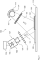
- Fig. 1 shows a schematic representation of a device 100 for testing a coating 101 of a document 103.
- the device 100 comprises an image sensor 105, an illumination device 107, a test structure 109, a holder 113 for the document 103, a processor 115, a reflective arrangement 117, a Display 119, an optical filter 123, a lens 121, an image camera 127 and a light source 125.
- the device 100 for testing the coating 101 of the document 103 includes the image sensor 105 and the lighting device 107 with the test structure 109, the lighting device 107 being designed to illuminate the test structure 109 in order to emit structured light in the direction of the document 103. Furthermore, the device 100 includes the holder 113 arranged in the beam path 111 of the structured light, into which the document 103 can be inserted in order to reflect the structured light through the document 103 in the direction of the image sensor 105, and the processor 115, which is designed, an image parameter to determine the image recording of the test structure, and to compare the image parameter with a reference parameter in order to test the coating 101 of the document 103.
- the document 103 can be one of the following documents 103: identity document, such as an ID card, passport, access control card, authorization card, company ID card, tax stamp or ticket, driver's license or vehicle ID card, means of payment, for example a bank card or credit card.
- identity document such as an ID card, passport, access control card, authorization card, company ID card, tax stamp or ticket, driver's license or vehicle ID card, means of payment, for example a bank card or credit card.
- the document 103 may include security features such as holograms, watermarks, microwriting, or optically variable ink.
- the document 103 can be single- or multi-layered or paper- and/or plastic-based.
- the document 103 can be constructed from plastic-based films, which are assembled into a card body by gluing and/or laminating, the films preferably having similar material properties.
- the document 103 can be made of polycarbonate.
- the coating 101 can be a layer of varnish or an application of varnish to protect the document 103 from wear and/or contamination and to increase its service life.
- the coating 101 can protect the document 103 from UV radiation.
- the coating 101 can be light-transparent or partially light-transparent.
- the lighting device 107 can include the light source 125, which is arranged in a housing.
- the housing can have a breakthrough on a side facing the test structure 109 for emitting a light beam directed onto the test structure 109.
- the test structure 109 can be arranged at this breakthrough.
- the holder 113 can include a storage area with a recess for the document 103. Furthermore, the holder can include a fastening device, for example a clip or an insert, for the document 103.
- the holder 113 can be arranged at such a distance from the lighting device 107 that the structured light illuminates the entire surface of the document 103 or only illuminates a specific area of the document 103, for example the area of a photograph.
- the processor 115 may be a microprocessor and may include memory. Furthermore, the processor 115 can be integrated into a data processing device connected to the device 100, for example a desktop computer or a laptop.
- the light source 125 may include an infrared light source, such as a thermal light source, an LED, or a laser.
- the thermal light source can be one Glow coil, a glow wire or a glow rod made of a heat-resistant material, for example tungsten or silicon carbide, which can emit infrared radiation particularly efficiently in the form of thermal radiation when heated above 1000 ° C.
- the lighting device 107 may include the reflective arrangement 117.
- the reflective arrangement 117 can be a parabolic mirror or a concave mirror, which partially encloses the lighting device 125.
- the reflective arrangement 117 may comprise a plurality of mirrors or reflectors which partially enclose the lighting device.
- the reflective arrangement 117 can align the light emitted by the light source 125 in the direction of the test structure 109 and the document 103, and thus increase the intensity of the light in the beam path 111.
- the test structure 109 can be a grid, in particular a line grid, which is designed as a transmission grid.
- the test structure in Fig. 1 is, for example, a transmission grating which is arranged in the beam path 111 between the light source 125 and the document.
- the structured light created when the radiation passes through the transmission grating can, after reflection on the document 103, be recorded in the image sensor 105 in order to obtain an image of the transmission grating.
- test structure 109 can be a reflection grating.
- This reflection grid can be arranged in the device 100 in such a way that at least part of the light generated by the light source 125 hits the reflection grid and is reflected as structured light in the direction of the document 103, the reflection of this light on the document 103 in the image sensor 105 can be recorded to obtain a recording of the reflection grating.
- the device 100 may include the optical filter 123 to filter or spectrally shape the structured light.
- the optical filter 123 can be arranged in the beam path 111 of the structured light, for example between the lighting device 107 and the document 103 or between the document 103 and the image sensor 105.
- the optical filter 123 may be a high-pass filter, a low-pass filter or a band-pass filter.
- the light source 125 is a thermal light source and the image sensor 105 is one infrared-sensitive image sensor 105, in particular a near-infrared-sensitive image sensor 105, the optical filter 123 can be a near-infrared-transmitting filter which, for example, filters out visible light, UV light, and/or middle and far infrared light from the beam path 111.
- the image sensor 105 can be a semiconductor sensor, in particular a CCD sensor.
- the semiconductor material of the sensor can be silicon or indium gallium arsenide.
- the device 100 may include the lens 121, wherein the lens 121 may be located in front of the image sensor 105.
- the objective 121 may include at least one lens and/or at least one mirror and/or at least one diffraction grating.
- the lens 121 can produce a focused image of the test structure 109 on the image sensor 105.
- the lens 121 can be arranged at a distance from the image sensor 105 that corresponds to the image width of the lens 121.
- the lens 121 can be designed and arranged in the device 100 in such a way that the size of the image of the test structure 109 corresponds to the size of the image sensor 105.
- an image parameter of the image can be determined particularly efficiently.
- the image sensor 105 and the lens 121 can be arranged in the image camera 127.
- the image camera 127 can be a digital camera, a digital SLR camera, or a smartphone with an integrated image sensor 105.
- the image camera 127 can be connected to a data processing device, for example a desktop computer or a laptop, to transmit the image recording.
- a data processing device for example a desktop computer or a laptop
- the device 100 may include a display 119 for indicating detection of the coating 101 or a coating defect.
- the display 119 can be a light display or a display, for example an LCD display, an OLED display or a film display.
- the display 119 can be integrated into the image camera 127 or a connected one Data processing device must be integrated.
- the display 119 can be connected to the processor 115.
- the image camera 127 may include the optical filter 123.
- the image camera 127 can include the processor 115 and the determination of the image parameter and the comparison with the reference parameter can take place in the image camera 127.
- Fig. 2a shows a schematic representation of a high-contrast image recording 201 of a test structure 109
- Fig. 2b shows a schematic representation of a low-contrast image recording 205 of a test structure 109.
- the high-contrast image recording 201 in Fig. 2a can be an image recording of a test structure 109, which was recorded with a document 103 without coating 101.
- the low-contrast image recording 205 in Fig. 2b can be a recording of the same test structure as in Fig. 2a be, which was recorded with a document 103 with coating 101.
- the contrast refers to differences in brightness in the image recordings, such as the difference between the dark grid lines 203 of the grid structure and the bright areas between these grid lines 203.
- the decrease in the contrast of the grid structure in Fig. 2b can also be perceived as a decrease in sharpness in the image capture.
- the loss of contrast in Fig. 2b lead to a widening of the grid lines 203 in the low-contrast image recording 205
- the test structures 109 in Fig. 2a and Fig. 2b are identical.
- the test structure 109 is a rectangular grid with horizontal and vertical grid lines 203.
- the round image of the rectangular grid corresponds to the part of the test structure 109 illuminated by the lighting device 107, which is imaged in focus on the image sensor 105.
- the round cross section can originate from a light beam with a round diameter generated by the lighting device 107.
- the loss of contrast in Fig. 2b can be caused by the coating 101 on the document 103.
- Reasons for the loss of contrast can be a surface roughness of the coating 101 and/or a shift in the focus of the image due to the beam path 111 shortened by the coating 101 and/or interference effects in the reflected structured light due to a superimposition of reflections on the top side of the coating and the bottom side of the coating
- the contrast loss can be used to test and/or detect the coating 101.
- the image recording can be evaluated with regard to an image parameter.
- the image parameter can be the image sharpness, the image contrast, or the image brightness, as well as a parameter calculated from at least one of these image parameters, for example a modulation transfer function or a Fourier transformation.
- a modulation of the brightness in the image recording can be analyzed.
- the image contrast is usually determined.
- the difference between the luminance of a dark structure in the image recording B D , for example the grid lines 203, and the luminance of a bright structure in the image recording B H , for example the bright area between the grid lines 203 can be determined.
- the image contrast can be a function of a spatial frequency.
- the image contrast can be a constant.
- the object contrast can correspond to the image contrast of the high-contrast image recording 201.
- the modulation transfer function is the ratio of the Image contrasts of the low-contrast image recording 205 and the high-contrast image recording 201.
- the coating 101 on the document 103 can be detected and/or checked by comparing the image parameters, for example the image contrasts and/or the modulation transfer functions, the low-contrast image recording 205 and the high-contrast image recording 201.
- image parameters for example the image contrasts and/or the modulation transfer functions, the low-contrast image recording 205 and the high-contrast image recording 201.
- an image parameter which was recorded with a coating-free reference surface can be used as a reference parameter.
- the processor 115 can store this reference parameter and compare a newly determined image parameter with the reference parameter for each new measurement.
- the processor 115 can be configured to detect a coating 101 if an image parameter of a document to be checked exceeds or falls below the reference parameter by a threshold value. Furthermore, the processor 115 can be configured to detect a coating error if the image parameter of the document 103 to be checked corresponds to the reference parameter or the deviation between the image parameter and the reference parameter falls below the threshold value.
- the processor 115 can be configured to detect a property of the coating 101, for example a minimum layer thickness of the coating 101, if the image parameter of a document 103 to be checked exceeds or falls below a further reference parameter. Furthermore, the processor 115 can be configured to determine a layer thickness of the coating 101 of the document 103 from the difference between the image parameter and the reference parameter.
- the image parameter can be assigned to an image section of the image recording and the processor 115 can be configured to determine a further image parameter of a further image section of the image recording of the test structure 109 and the image parameter and the further image parameter with the Compare reference parameters.
- the processor can check the distribution and/or the homogeneity of a layer thickness of the coating 101 of the document 103.
- Fig. 3 shows a schematic representation of the device 100 for testing the coating 101 of the document 103 according to an embodiment in which at least one uncoated reference surface 129 adjacent to the document 103 can or is inserted into the holder 113.
- a reference environment or a reference for determining the reference parameter can be created.
- the uncoated reference surface 129 can be in the form of an uncoated document.
- the uncoated reference surface 129 and the document 103 can be arranged in the beam path 111 of the structured light in such a way that a first image section of the image recording is assigned to the document 103 and a second image section of the image recording is assigned to the uncoated reference surface 129.
- the image parameter and the reference parameter are determined simultaneously or differentially from the image recording.
- the image parameter and the reference parameter are determined from an image recording, or the image parameter is determined from a first image recording and the reference parameter is determined from a second image recording.
- the spatial resolution of the image parameter can be influenced by a structure size of the test structure 109. Furthermore, by reducing the structure size of the test structure 109, for example by a Reducing the distances between the grid lines 203 of a grid, the spatial resolution of the image parameter can be increased.
Landscapes
- Engineering & Computer Science (AREA)
- Physics & Mathematics (AREA)
- General Physics & Mathematics (AREA)
- General Health & Medical Sciences (AREA)
- Health & Medical Sciences (AREA)
- Chemical & Material Sciences (AREA)
- Biochemistry (AREA)
- Analytical Chemistry (AREA)
- Life Sciences & Earth Sciences (AREA)
- Immunology (AREA)
- Pathology (AREA)
- Quality & Reliability (AREA)
- Computer Vision & Pattern Recognition (AREA)
- Theoretical Computer Science (AREA)
- Toxicology (AREA)
- Mathematical Physics (AREA)
- Investigating Materials By The Use Of Optical Means Adapted For Particular Applications (AREA)
Claims (15)
- Dispositif (100) pour tester un revêtement (101) d'un document (103), comprenant:un capteur d'image (105);un dispositif d'éclairage (107) comprenant une structure de test (109), dans lequel le dispositif d'éclairage (107) est configuré pour éclairer la structure de test (109) afin d'émettre une lumière structurée en direction du document (103);un support (113) disposé dans le trajet du faisceau (111) de la lumière structurée, support dans lequel le document (103) peut être inséré afin de réfléchir la lumière structurée à travers le document (103) en direction du capteur d'image (105);un processeur (115), qui est configuré pour déterminer un paramètre d'image de l'enregistrement d'image de la structure de test (109) et pour comparer le paramètre d'image avec un paramètre de référence afin de tester le revêtement (101) du document (103),dans lequel la structure de test (109) est une grille,dans lequel le processeur (115) est configuré pour détecter le revêtement (101) si le paramètre d'image et le paramètre de référence sont différents,dans lequel le processeur (115) est configuré pour déterminer une épaisseur de couche du revêtement (101) du document (103) à partir de la différence entre le paramètre d'image et le paramètre de référence,dans lequel le paramètre d'image est affecté à une section d'image de l'enregistrement d'image, dans lequel le processeur (115) est configuré pour déterminer un autre paramètre d'image d'une autre section d'image de l'enregistrement d'image de la structure de test (109), et dans lequel le processeur (115) est configuré pour comparer le paramètre d'image et l'autre paramètre d'image avec le paramètre de référence afin de tester la répartition ou l'homogénéité d'une épaisseur de couche du revêtement (101) du document (103),dans lequel au moins une surface de référence non revêtue (129) peut être insérée dans le support (113) adjacent au document, dans lequel une première section d'image de l'enregistrement d'image est attribuée au document (103), dans lequel une deuxième section d'image de l'image l'enregistrement est attribué à la surface de référence non revêtue (129), et dans lequel le processeur (115) est configuré pour déterminer le paramètre de référence en tant que paramètre d'image de la deuxième section d'image, dans lequel la surface de référence non revêtue (129) est un document sans revêtement,où le paramètre d'image respectif est le paramètre d'image suivant: fonction de transfert de modulation,dans lequel le processeur (115) est configuré pour déterminer une perte de contraste dans l'image de la structure de test (109), dans lequel le processeur (115) est configuré pour analyser une courbe de contraste dans l'image de la structure de test (115) pour cette dans ce but, dans lequel cette analyse est effectuée avec le document avec le revêtement (101) et avec le document sans revêtement, dans lequel le paramètre d'image de la au moins une surface de référence non revêtue (129) est utilisé comme paramètre de référence dans cette analyse.
- Dispositif (100) selon la revendication 1, dans lequel le dispositif d'éclairage (107) comprend une source de lumière infrarouge, notamment une source de lumière infrarouge thermique, et dans lequel le capteur d'image (105) est un capteur d'image sensible à l'infrarouge (105).
- Dispositif (100) selon la revendication 1 ou 2, dans lequel le dispositif d'éclairage (107) comprend un agencement réfléchissant (117), notamment un agencement de miroirs paraboliques, pour aligner la lumière structurée.
- Dispositif (100) selon l'une quelconque des revendications précédentes, dans lequel la grille est une grille de transmission ou une grille de lignes à interligne constant ou variable.
- Dispositif (100) selon l'une quelconque des revendications précédentes, dans lequel le dispositif (100) comprend un filtre optique (123), notamment un filtre passe-haut, un filtre passe-bas ou un filtre passe-bande, afin de filtrer ou mettre en forme spectralement la lumière structurée.
- Dispositif (100) selon l'une quelconque des revendications précédentes, dans lequel le dispositif comprend une lentille (121) qui est devant le capteur d'image (105) et avec laquelle lentille une image focalisée de la structure de test peut être générée. sur le capteur d'image.
- Dispositif (100) selon l'une quelconque des revendications précédentes, dans lequel le processeur (115) est configuré pour détecter le revêtement (101) si le paramètre d'image est inférieur au paramètre de référence.
- Dispositif (100) selon l'une quelconque des revendications précédentes, dans lequel le dispositif comprend un affichage (119) pour afficher une détection du revêtement (101) ou un défaut de revêtement.
- Dispositif (100) selon l'une quelconque des revendications précédentes, dans lequel le paramètre d'image respectif est au moins l'un des paramètres d'image suivants: netteté d'image, contraste d'image, luminosité d'image, transformation de Fourier.
- Procédé pour tester un revêtement (101) d'un document (103), comprenant:éclairer une structure de test (109) pour émettre une lumière structurée en direction du document (103);réfléchir la lumière structurée à travers le document (103) en direction d'un capteur d'image (105);enregistrer la lumière structurée réfléchie avec un capteur d'image (105) afin d'obtenir un enregistrement d'image de la structure de test (109);déterminer un paramètre d'image de l'enregistrement d'image; etcomparer le paramètre d'image à un paramètre de référence pour tester le revêtement (101) du document (103),dans lequel la structure de test (109) est une grille,dans lequel le revêtement (101) est détecté si le paramètre d'image et le paramètre de référence sont différents,dans lequel une épaisseur de couche du revêtement du document est déterminée à partir de la différence entre le paramètre d'image et le paramètre de référence,dans lequel le paramètre d'image est affecté à une section d'image de l'enregistrement d'image, dans lequel un autre paramètre d'image d'une deuxième section d'image de l'enregistrement d'image de la structure de test (109) est déterminé, et dans lequel le paramètre d'image et l'autre paramètre d'image sont comparé au paramètre de référence pour tester la répartition ou l'homogénéité d'une épaisseur de couche du revêtement (101) du document (103),dans lequel le paramètre de référence est un paramètre d'image d'un enregistrement d'image d'une surface de référence non revêtue (129), dans lequel la surface de référence non revêtue (129) est un document sans revêtement,dans lequel au moins une surface de référence non revêtue (129) est agencée adjacente au document, dans lequel une première section d'image de l'enregistrement d'image est attribuée au document, dans lequel une deuxième section d'image de l'enregistrement d'image est attribuée à la zone de référence non revêtue (129), et dans lequel le paramètre de référence est déterminé en tant que paramètre d'image de la deuxième section d'image,où le paramètre d'image respectif est au moins l'un des paramètres d'image suivants: fonction de transfert de modulation,
dans lequel une perte de contraste dans l'image de la structure de test (109) est déterminée, dans lequel une courbe de contraste est déterminée dans l'image de la structure de test (115) à cet effet, dans lequel cette analyse est effectuée avec le document avec le revêtement (101) et avec le document sans revêtement, dans lequel le paramètre d'image de la au moins une surface de référence non revêtue (129) est utilisé comme paramètre de référence dans cette analyse. - Procédé selon la revendication 10, dans lequel le paramètre de référence est un paramètre d'image d'un enregistrement d'image du document d'identification sans revêtement.
- Procédé selon la revendication 10 ou 11, dans lequel la grille est une grille de transmission ou une grille de lignes à interligne constant ou variable.
- Procédé selon l'une quelconque des revendications 10 à 12, dans lequel la lumière structurée est filtrée ou mise en forme spectralement avec un filtre optique (123), notamment un filtre passe-haut, un filtre passe-bas ou un filtre passe-bande..
- Procédé selon l'une quelconque des revendications 10 à 13, dans lequel une lentille (121) est devant le capteur d'image (105) avec laquelle lentille une image focalisée de la structure de test (109) est générée sur le capteur d'image (105).
- Procédé selon l'une quelconque des revendications 10 à 14, dans lequel le revêtement (101) est détecté si le paramètre d'image est inférieur au paramètre de référence.
Applications Claiming Priority (1)
| Application Number | Priority Date | Filing Date | Title |
|---|---|---|---|
| DE102015113469.1A DE102015113469A1 (de) | 2015-08-14 | 2015-08-14 | Vorrichtung zum Prüfen einer Beschichtung eines Dokumentes |
Publications (2)
| Publication Number | Publication Date |
|---|---|
| EP3131070A1 EP3131070A1 (fr) | 2017-02-15 |
| EP3131070B1 true EP3131070B1 (fr) | 2023-10-11 |
Family
ID=56888909
Family Applications (1)
| Application Number | Title | Priority Date | Filing Date |
|---|---|---|---|
| EP16184003.8A Active EP3131070B1 (fr) | 2015-08-14 | 2016-08-12 | Dispositif de controle d'un revetement d'un document |
Country Status (2)
| Country | Link |
|---|---|
| EP (1) | EP3131070B1 (fr) |
| DE (1) | DE102015113469A1 (fr) |
Families Citing this family (4)
| Publication number | Priority date | Publication date | Assignee | Title |
|---|---|---|---|---|
| DE102017120035A1 (de) * | 2017-08-07 | 2019-02-07 | Bw Papersystems Hamburg Gmbh | Verfahren und Prüfvorrichtung zum Prüfen der Qualität von Ergebnissen der mechanischen Bearbeitung eines Bogens |
| CN110823515B (zh) * | 2018-08-14 | 2022-02-01 | 宁波舜宇光电信息有限公司 | 一种结构光投射模组多工位检测装置及其检测方法 |
| CN109738157A (zh) * | 2018-12-11 | 2019-05-10 | 信利光电股份有限公司 | 结构光投影器的视场角检测方法、装置及可读存储介质 |
| CN111750785B (zh) * | 2020-07-03 | 2021-08-24 | 重庆科技学院 | 一种包衣厚度和包衣质量的在线测量方法及测量装置 |
Family Cites Families (6)
| Publication number | Priority date | Publication date | Assignee | Title |
|---|---|---|---|---|
| DE2055594A1 (de) * | 1969-11-13 | 1971-07-08 | Sira Instiute | Verfahren und Vorrichtung zum Betrach ten von Gegenstanden |
| US4183665A (en) * | 1977-12-07 | 1980-01-15 | Ardac, Inc. | Apparatus for testing the presence of color in a paper security |
| US6639201B2 (en) * | 2001-11-07 | 2003-10-28 | Applied Materials, Inc. | Spot grid array imaging system |
| EP1496479A1 (fr) * | 2003-07-08 | 2005-01-12 | Identification Systems DERMALOG GmbH | Dispositif de lecture pour la vérification automatique de documents |
| DE102009037553A1 (de) * | 2009-08-17 | 2011-02-24 | Baumer Innotec Ag | Detektion von transparenten Schutzschichten auf Substraten |
| DE102011051781A1 (de) * | 2011-07-12 | 2013-01-17 | Göpel electronic GmbH | Deflektometrische Anordnung zur Oberflächeninspektion |
-
2015
- 2015-08-14 DE DE102015113469.1A patent/DE102015113469A1/de not_active Withdrawn
-
2016
- 2016-08-12 EP EP16184003.8A patent/EP3131070B1/fr active Active
Also Published As
| Publication number | Publication date |
|---|---|
| DE102015113469A1 (de) | 2017-02-16 |
| EP3131070A1 (fr) | 2017-02-15 |
Similar Documents
| Publication | Publication Date | Title |
|---|---|---|
| DE19924750C2 (de) | Leseanordnung für Informationsstreifen mit optisch kodierter Information | |
| EP3131070B1 (fr) | Dispositif de controle d'un revetement d'un document | |
| EP3555811A2 (fr) | Vérification d'un document de sécurité | |
| EP2577620B1 (fr) | Dispositif de contrôle de l'authenticité de documents de valeur | |
| EP3286740A1 (fr) | Procédé d'identification d'un motif de sécurité par reconstruction 3d artificielle | |
| DE102006053788A1 (de) | Verfahren zur Erkennung von Verschmutzungen im Bereich von Farbübergängen auf Wertdokumenten und Mittel zur Durchführung des Verfahrens | |
| WO2004013817A2 (fr) | Dispositif et procede de traitement de documents de valeur | |
| DE102017102556A1 (de) | Verfahren zur Verifizierung eines Sicherheitsdokuments sowie ein Sicherheitsdokument, eine Vorrichtung und ein Sicherheitselement | |
| EP2380146B1 (fr) | Procédé et dispositif de vérification de documents de valeur | |
| DE102011005518A1 (de) | Sicherheitselement mit einem 3D-Farbeffekt sowie Verifikationsverfahren und Verifikationsvorrichtung für ein solches Sicherheitselement | |
| EP3782136B1 (fr) | Procédé de vérification d'un signe de sécurité à base de luminophore | |
| EP3047461B1 (fr) | Appareil de verification de documents | |
| DE69418887T2 (de) | Sicherheitsleser zur automatischen erfassung von verfälschungen und änderungen | |
| DE102013103527A1 (de) | Bildaufnahmesystem zur Bildaufnahme von Merkmalen eines Identifikationsdokumentes | |
| DE102013103522A1 (de) | Bildaufnahmesystem zur Bildaufnahme eines Merkmals eines Identifikationsdokumentes | |
| DE102020108117A1 (de) | TIRFM-fähiges Mikroskop und Verfahren zum Betreiben eines TIRFM-fähigen Mikroskops | |
| EP3841524B1 (fr) | Procédé de contrôle et dispositif de contrôle destinés au contrôle de marquages de sécurité | |
| DE102014113188B4 (de) | Digitales Mikroskop und Verfahren zu dessen Inbetriebnahme | |
| EP1197926B1 (fr) | Procédé de détection de relief de pièces de monnaie dans des machines actionnées par des pièces de monnaie | |
| US10839634B2 (en) | Taggant system | |
| EP2473979B1 (fr) | Dispositif de vérification pour documents de valeur et/ou de sécurité double face | |
| DE102014204302A1 (de) | Vorrichtung und Verfahren zur Prüfung mindestens eines Sicherheitselements eines Sicherheitsdokuments | |
| DE102004005246B4 (de) | Vorrichtung und Verfahren zur Überwachung eines Leimauftrages auf ein Substrat | |
| WO2017182479A1 (fr) | Dispositif et procédé de surveillance de caractéristiques de sécurité en couleur | |
| DE10054099B4 (de) | Verfahren und Vorrichtung zum Bestimmen von Defektenauf oder in einem Gegenstand |
Legal Events
| Date | Code | Title | Description |
|---|---|---|---|
| PUAI | Public reference made under article 153(3) epc to a published international application that has entered the european phase |
Free format text: ORIGINAL CODE: 0009012 |
|
| STAA | Information on the status of an ep patent application or granted ep patent |
Free format text: STATUS: THE APPLICATION HAS BEEN PUBLISHED |
|
| AK | Designated contracting states |
Kind code of ref document: A1 Designated state(s): AL AT BE BG CH CY CZ DE DK EE ES FI FR GB GR HR HU IE IS IT LI LT LU LV MC MK MT NL NO PL PT RO RS SE SI SK SM TR |
|
| AX | Request for extension of the european patent |
Extension state: BA ME |
|
| STAA | Information on the status of an ep patent application or granted ep patent |
Free format text: STATUS: REQUEST FOR EXAMINATION WAS MADE |
|
| 17P | Request for examination filed |
Effective date: 20170726 |
|
| RBV | Designated contracting states (corrected) |
Designated state(s): AL AT BE BG CH CY CZ DE DK EE ES FI FR GB GR HR HU IE IS IT LI LT LU LV MC MK MT NL NO PL PT RO RS SE SI SK SM TR |
|
| STAA | Information on the status of an ep patent application or granted ep patent |
Free format text: STATUS: EXAMINATION IS IN PROGRESS |
|
| 17Q | First examination report despatched |
Effective date: 20200309 |
|
| GRAP | Despatch of communication of intention to grant a patent |
Free format text: ORIGINAL CODE: EPIDOSNIGR1 |
|
| STAA | Information on the status of an ep patent application or granted ep patent |
Free format text: STATUS: GRANT OF PATENT IS INTENDED |
|
| RIC1 | Information provided on ipc code assigned before grant |
Ipc: G01N 21/958 20060101ALI20230330BHEP Ipc: G07D 7/12 20160101ALI20230330BHEP Ipc: G06T 7/00 20170101ALI20230330BHEP Ipc: G01N 21/84 20060101ALI20230330BHEP Ipc: G01N 21/25 20060101ALI20230330BHEP Ipc: G01N 21/00 20060101ALI20230330BHEP Ipc: G07D 7/20 20160101AFI20230330BHEP |
|
| INTG | Intention to grant announced |
Effective date: 20230502 |
|
| P01 | Opt-out of the competence of the unified patent court (upc) registered |
Effective date: 20230526 |
|
| GRAS | Grant fee paid |
Free format text: ORIGINAL CODE: EPIDOSNIGR3 |
|
| GRAA | (expected) grant |
Free format text: ORIGINAL CODE: 0009210 |
|
| STAA | Information on the status of an ep patent application or granted ep patent |
Free format text: STATUS: THE PATENT HAS BEEN GRANTED |
|
| AK | Designated contracting states |
Kind code of ref document: B1 Designated state(s): AL AT BE BG CH CY CZ DE DK EE ES FI FR GB GR HR HU IE IS IT LI LT LU LV MC MK MT NL NO PL PT RO RS SE SI SK SM TR |
|
| REG | Reference to a national code |
Ref country code: GB Ref legal event code: FG4D Free format text: NOT ENGLISH |
|
| REG | Reference to a national code |
Ref country code: CH Ref legal event code: EP |
|
| REG | Reference to a national code |
Ref country code: DE Ref legal event code: R096 Ref document number: 502016016145 Country of ref document: DE |
|
| REG | Reference to a national code |
Ref country code: IE Ref legal event code: FG4D Free format text: LANGUAGE OF EP DOCUMENT: GERMAN |
|
| REG | Reference to a national code |
Ref country code: LT Ref legal event code: MG9D |
|
| REG | Reference to a national code |
Ref country code: NL Ref legal event code: MP Effective date: 20231011 |
|
| PG25 | Lapsed in a contracting state [announced via postgrant information from national office to epo] |
Ref country code: NL Free format text: LAPSE BECAUSE OF FAILURE TO SUBMIT A TRANSLATION OF THE DESCRIPTION OR TO PAY THE FEE WITHIN THE PRESCRIBED TIME-LIMIT Effective date: 20231011 |
|
| PG25 | Lapsed in a contracting state [announced via postgrant information from national office to epo] |
Ref country code: GR Free format text: LAPSE BECAUSE OF FAILURE TO SUBMIT A TRANSLATION OF THE DESCRIPTION OR TO PAY THE FEE WITHIN THE PRESCRIBED TIME-LIMIT Effective date: 20240112 |
|
| PG25 | Lapsed in a contracting state [announced via postgrant information from national office to epo] |
Ref country code: IS Free format text: LAPSE BECAUSE OF FAILURE TO SUBMIT A TRANSLATION OF THE DESCRIPTION OR TO PAY THE FEE WITHIN THE PRESCRIBED TIME-LIMIT Effective date: 20240211 |
|
| PG25 | Lapsed in a contracting state [announced via postgrant information from national office to epo] |
Ref country code: LT Free format text: LAPSE BECAUSE OF FAILURE TO SUBMIT A TRANSLATION OF THE DESCRIPTION OR TO PAY THE FEE WITHIN THE PRESCRIBED TIME-LIMIT Effective date: 20231011 |
|
| PG25 | Lapsed in a contracting state [announced via postgrant information from national office to epo] |
Ref country code: ES Free format text: LAPSE BECAUSE OF FAILURE TO SUBMIT A TRANSLATION OF THE DESCRIPTION OR TO PAY THE FEE WITHIN THE PRESCRIBED TIME-LIMIT Effective date: 20231011 |
|
| PG25 | Lapsed in a contracting state [announced via postgrant information from national office to epo] |
Ref country code: LT Free format text: LAPSE BECAUSE OF FAILURE TO SUBMIT A TRANSLATION OF THE DESCRIPTION OR TO PAY THE FEE WITHIN THE PRESCRIBED TIME-LIMIT Effective date: 20231011 Ref country code: IS Free format text: LAPSE BECAUSE OF FAILURE TO SUBMIT A TRANSLATION OF THE DESCRIPTION OR TO PAY THE FEE WITHIN THE PRESCRIBED TIME-LIMIT Effective date: 20240211 Ref country code: GR Free format text: LAPSE BECAUSE OF FAILURE TO SUBMIT A TRANSLATION OF THE DESCRIPTION OR TO PAY THE FEE WITHIN THE PRESCRIBED TIME-LIMIT Effective date: 20240112 Ref country code: ES Free format text: LAPSE BECAUSE OF FAILURE TO SUBMIT A TRANSLATION OF THE DESCRIPTION OR TO PAY THE FEE WITHIN THE PRESCRIBED TIME-LIMIT Effective date: 20231011 Ref country code: BG Free format text: LAPSE BECAUSE OF FAILURE TO SUBMIT A TRANSLATION OF THE DESCRIPTION OR TO PAY THE FEE WITHIN THE PRESCRIBED TIME-LIMIT Effective date: 20240111 Ref country code: PT Free format text: LAPSE BECAUSE OF FAILURE TO SUBMIT A TRANSLATION OF THE DESCRIPTION OR TO PAY THE FEE WITHIN THE PRESCRIBED TIME-LIMIT Effective date: 20240212 |
|
| PG25 | Lapsed in a contracting state [announced via postgrant information from national office to epo] |
Ref country code: SE Free format text: LAPSE BECAUSE OF FAILURE TO SUBMIT A TRANSLATION OF THE DESCRIPTION OR TO PAY THE FEE WITHIN THE PRESCRIBED TIME-LIMIT Effective date: 20231011 Ref country code: RS Free format text: LAPSE BECAUSE OF FAILURE TO SUBMIT A TRANSLATION OF THE DESCRIPTION OR TO PAY THE FEE WITHIN THE PRESCRIBED TIME-LIMIT Effective date: 20231011 Ref country code: PL Free format text: LAPSE BECAUSE OF FAILURE TO SUBMIT A TRANSLATION OF THE DESCRIPTION OR TO PAY THE FEE WITHIN THE PRESCRIBED TIME-LIMIT Effective date: 20231011 Ref country code: NO Free format text: LAPSE BECAUSE OF FAILURE TO SUBMIT A TRANSLATION OF THE DESCRIPTION OR TO PAY THE FEE WITHIN THE PRESCRIBED TIME-LIMIT Effective date: 20240111 Ref country code: LV Free format text: LAPSE BECAUSE OF FAILURE TO SUBMIT A TRANSLATION OF THE DESCRIPTION OR TO PAY THE FEE WITHIN THE PRESCRIBED TIME-LIMIT Effective date: 20231011 Ref country code: HR Free format text: LAPSE BECAUSE OF FAILURE TO SUBMIT A TRANSLATION OF THE DESCRIPTION OR TO PAY THE FEE WITHIN THE PRESCRIBED TIME-LIMIT Effective date: 20231011 |
|
| PG25 | Lapsed in a contracting state [announced via postgrant information from national office to epo] |
Ref country code: DK Free format text: LAPSE BECAUSE OF FAILURE TO SUBMIT A TRANSLATION OF THE DESCRIPTION OR TO PAY THE FEE WITHIN THE PRESCRIBED TIME-LIMIT Effective date: 20231011 |
|
| REG | Reference to a national code |
Ref country code: DE Ref legal event code: R097 Ref document number: 502016016145 Country of ref document: DE |
|
| PG25 | Lapsed in a contracting state [announced via postgrant information from national office to epo] |
Ref country code: CZ Free format text: LAPSE BECAUSE OF FAILURE TO SUBMIT A TRANSLATION OF THE DESCRIPTION OR TO PAY THE FEE WITHIN THE PRESCRIBED TIME-LIMIT Effective date: 20231011 |
|
| PG25 | Lapsed in a contracting state [announced via postgrant information from national office to epo] |
Ref country code: SK Free format text: LAPSE BECAUSE OF FAILURE TO SUBMIT A TRANSLATION OF THE DESCRIPTION OR TO PAY THE FEE WITHIN THE PRESCRIBED TIME-LIMIT Effective date: 20231011 |
|
| PG25 | Lapsed in a contracting state [announced via postgrant information from national office to epo] |
Ref country code: SM Free format text: LAPSE BECAUSE OF FAILURE TO SUBMIT A TRANSLATION OF THE DESCRIPTION OR TO PAY THE FEE WITHIN THE PRESCRIBED TIME-LIMIT Effective date: 20231011 Ref country code: SK Free format text: LAPSE BECAUSE OF FAILURE TO SUBMIT A TRANSLATION OF THE DESCRIPTION OR TO PAY THE FEE WITHIN THE PRESCRIBED TIME-LIMIT Effective date: 20231011 Ref country code: RO Free format text: LAPSE BECAUSE OF FAILURE TO SUBMIT A TRANSLATION OF THE DESCRIPTION OR TO PAY THE FEE WITHIN THE PRESCRIBED TIME-LIMIT Effective date: 20231011 Ref country code: IT Free format text: LAPSE BECAUSE OF FAILURE TO SUBMIT A TRANSLATION OF THE DESCRIPTION OR TO PAY THE FEE WITHIN THE PRESCRIBED TIME-LIMIT Effective date: 20231011 Ref country code: EE Free format text: LAPSE BECAUSE OF FAILURE TO SUBMIT A TRANSLATION OF THE DESCRIPTION OR TO PAY THE FEE WITHIN THE PRESCRIBED TIME-LIMIT Effective date: 20231011 Ref country code: DK Free format text: LAPSE BECAUSE OF FAILURE TO SUBMIT A TRANSLATION OF THE DESCRIPTION OR TO PAY THE FEE WITHIN THE PRESCRIBED TIME-LIMIT Effective date: 20231011 Ref country code: CZ Free format text: LAPSE BECAUSE OF FAILURE TO SUBMIT A TRANSLATION OF THE DESCRIPTION OR TO PAY THE FEE WITHIN THE PRESCRIBED TIME-LIMIT Effective date: 20231011 |
|
| PLBE | No opposition filed within time limit |
Free format text: ORIGINAL CODE: 0009261 |
|
| STAA | Information on the status of an ep patent application or granted ep patent |
Free format text: STATUS: NO OPPOSITION FILED WITHIN TIME LIMIT |
|
| 26N | No opposition filed |
Effective date: 20240712 |
|
| PG25 | Lapsed in a contracting state [announced via postgrant information from national office to epo] |
Ref country code: SI Free format text: LAPSE BECAUSE OF FAILURE TO SUBMIT A TRANSLATION OF THE DESCRIPTION OR TO PAY THE FEE WITHIN THE PRESCRIBED TIME-LIMIT Effective date: 20231011 |
|
| PG25 | Lapsed in a contracting state [announced via postgrant information from national office to epo] |
Ref country code: SI Free format text: LAPSE BECAUSE OF FAILURE TO SUBMIT A TRANSLATION OF THE DESCRIPTION OR TO PAY THE FEE WITHIN THE PRESCRIBED TIME-LIMIT Effective date: 20231011 |
|
| REG | Reference to a national code |
Ref country code: CH Ref legal event code: PL |
|
| PG25 | Lapsed in a contracting state [announced via postgrant information from national office to epo] |
Ref country code: LU Free format text: LAPSE BECAUSE OF NON-PAYMENT OF DUE FEES Effective date: 20240812 |
|
| PG25 | Lapsed in a contracting state [announced via postgrant information from national office to epo] |
Ref country code: CH Free format text: LAPSE BECAUSE OF NON-PAYMENT OF DUE FEES Effective date: 20240831 Ref country code: MC Free format text: LAPSE BECAUSE OF FAILURE TO SUBMIT A TRANSLATION OF THE DESCRIPTION OR TO PAY THE FEE WITHIN THE PRESCRIBED TIME-LIMIT Effective date: 20231011 |
|
| REG | Reference to a national code |
Ref country code: BE Ref legal event code: MM Effective date: 20240831 |
|
| PG25 | Lapsed in a contracting state [announced via postgrant information from national office to epo] |
Ref country code: BE Free format text: LAPSE BECAUSE OF NON-PAYMENT OF DUE FEES Effective date: 20240831 |
|
| PG25 | Lapsed in a contracting state [announced via postgrant information from national office to epo] |
Ref country code: IE Free format text: LAPSE BECAUSE OF NON-PAYMENT OF DUE FEES Effective date: 20240812 |
|
| PG25 | Lapsed in a contracting state [announced via postgrant information from national office to epo] |
Ref country code: FI Free format text: LAPSE BECAUSE OF FAILURE TO SUBMIT A TRANSLATION OF THE DESCRIPTION OR TO PAY THE FEE WITHIN THE PRESCRIBED TIME-LIMIT Effective date: 20231011 |
|
| PGFP | Annual fee paid to national office [announced via postgrant information from national office to epo] |
Ref country code: DE Payment date: 20250819 Year of fee payment: 10 |
|
| REG | Reference to a national code |
Ref country code: AT Ref legal event code: MM01 Ref document number: 1621011 Country of ref document: AT Kind code of ref document: T Effective date: 20240812 |
|
| PGFP | Annual fee paid to national office [announced via postgrant information from national office to epo] |
Ref country code: GB Payment date: 20250822 Year of fee payment: 10 |
|
| PG25 | Lapsed in a contracting state [announced via postgrant information from national office to epo] |
Ref country code: AT Free format text: LAPSE BECAUSE OF NON-PAYMENT OF DUE FEES Effective date: 20240812 |
|
| PGFP | Annual fee paid to national office [announced via postgrant information from national office to epo] |
Ref country code: FR Payment date: 20250821 Year of fee payment: 10 |
|
| PG25 | Lapsed in a contracting state [announced via postgrant information from national office to epo] |
Ref country code: CY Free format text: LAPSE BECAUSE OF FAILURE TO SUBMIT A TRANSLATION OF THE DESCRIPTION OR TO PAY THE FEE WITHIN THE PRESCRIBED TIME-LIMIT; INVALID AB INITIO Effective date: 20160812 |
|
| PG25 | Lapsed in a contracting state [announced via postgrant information from national office to epo] |
Ref country code: HU Free format text: LAPSE BECAUSE OF FAILURE TO SUBMIT A TRANSLATION OF THE DESCRIPTION OR TO PAY THE FEE WITHIN THE PRESCRIBED TIME-LIMIT; INVALID AB INITIO Effective date: 20160812 |