EP3131111A1 - Elektronische schaltvorrichtung mit keramischen materialien - Google Patents
Elektronische schaltvorrichtung mit keramischen materialien Download PDFInfo
- Publication number
- EP3131111A1 EP3131111A1 EP15180837.5A EP15180837A EP3131111A1 EP 3131111 A1 EP3131111 A1 EP 3131111A1 EP 15180837 A EP15180837 A EP 15180837A EP 3131111 A1 EP3131111 A1 EP 3131111A1
- Authority
- EP
- European Patent Office
- Prior art keywords
- half portion
- composite material
- electronic switch
- switch device
- receiving chamber
- Prior art date
- Legal status (The legal status is an assumption and is not a legal conclusion. Google has not performed a legal analysis and makes no representation as to the accuracy of the status listed.)
- Granted
Links
Images







Classifications
-
- H—ELECTRICITY
- H01—ELECTRIC ELEMENTS
- H01H—ELECTRIC SWITCHES; RELAYS; SELECTORS; EMERGENCY PROTECTIVE DEVICES
- H01H50/00—Details of electromagnetic relays
- H01H50/02—Bases; Casings; Covers
Definitions
- the present invention relates to an electronic switch device with ceramic materials, and especially relates to an electronic element capable for controlling the circuit ON or OFF. It may prevent the sparkles generated by the current from contacting the non-metal part and further reduce the occurrence of melting and burning the non-metal part to prevent from influencing the operation of the current.
- the circuit board is the core which may operate with other electronic elements to make the whole instruments operate smoothly.
- the electronic elements are the basic part in the electronic circuit. They are individually packaging in general and each of them has two or more leads or metal pads. The electronic elements must connect with one another to form an electronic circuit with a specific function, such as the amplifier, the radio receiver, and the oscillator.
- the general method of connecting with the electronic elements is melting.
- the electronic elements may be individually packaged by each (resistor, capacitor, inductor, diode, and etc.), or the group with various complexities, such as integrated circuit (operational amplifier, network resistor, logic gate).
- the electronic elements may be classified into terminal and connector (for electrical connection device), power cord (for connecting interface or end terminal), switch (capable for controlling the electronic elements ON or OFF), resistor (electronic elements with resistance), protection device (passive elements mounted on the protection circuit in higher voltage or current), capacitor (the elements may storage the electric charges in electric field for filtering, the capacitor may normally change the alternating voltage but not change the constant direct voltage), electro-magnetic sensing device (the electronic elements with magnetism), network (composite electronic element composed of many or many kinds of passive components), memristor, piezoelectric device and crystal resonator (the passive element with Piezoelectricity), power source (current source), sensor, and etc.
- the most of above mentioned electronic elements may be packaged by the resin dispensing, especially for the electronic switch elements to isolate and protect from being influenced by the environment.
- the sparkles are generated while the current is ON and two electrically conductive ends are separated from each other.
- the sparkles may damage the electronic elements, they may also melt and burn the plastic housing which is formed after packaging the electronic element (such like relay, socket of each electronic element, timer, and etc.).
- the cause of fire may be caused by the sparkles generated from the electronic elements arranged inside the electronic device.
- the package made by resin dispensing may improve the insulating quality, it is not heat-resisting and the resin dispensing may become brittle and hard to have better insulation.
- the sparkles may still damage the plastic housing and the inside components.
- An object of this invention is providing an electronic switch device with ceramic materials for preventing from sparkling to contact the plastic housing of the electric elements to result in melting, burning, and further fire and protecting the operation of the components arranged inside the electronic elements while the current is ON and two electrically conductive ends are separated from each other compared to the conventional electronic switch elements.
- the electronic switch device may comprise a housing, having a first half portion and a second half portion, and a receiving chamber is defined by the first half portion and the second half portion; a detenting assembly, received in the receiving chamber and arranged in the second half portion; and an isolating composite material, arranged at one side surface of the second half portion corresponding to the receiving chamber, the isolating composite material is isolated the contact between the second half portion and the detenting assembly.
- the isolating composite material is a ceramic sheet and covered on the side surface of the second half portion corresponding to the receiving chamber.
- the isolating composite material is a ceramic powder and coated on the side surface of the second half portion corresponding to the receiving chamber.
- the isolating composite material is a ceramic powder and coated on an inner side surface and an outer surface of the second half portion.
- the detenting assembly further includes a magnetic coil portion and an electrically conductive metal portion.
- the isolating composite material is further arranged at one side surface of the first half portion corresponding to the receiving chamber.
- the electronic switch device may comprise a housing, having a first half portion and a second half portion, and a receiving chamber is defined by the first half portion and the second half portion; a detenting assembly, received in the receiving chamber and arranged in the second half portion; and an isolating composite material, arranged at one side surface of the first half portion corresponding to the receiving chamber, the isolating composite material is isolated the contact between the first half portion and the detenting assembly.
- the isolating composite material is a ceramic sheet and covered on the side of the first half portion corresponding to the receiving chamber.
- the isolating composite material is a ceramic powder and coated on the side surface of the first half portion corresponding to the receiving chamber.
- the isolating composite material is further arranged at one side surface of the second half portion corresponding to the receiving chamber.
- the advantage is that the arrangement of the isolating composite material may ensure to prevent the sparkles from damaging the first half portion and the second half portion when the current is ON and two electrically conductive ends are separated from each other, ensure the smooth operation of the detenting assembly, and reduce the risk of disaster.
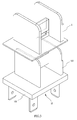
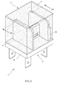
- an electronic switch device with ceramic composite materials of present invention may comprise a housing 1, a detenting assembly 2, and an isolating composite material 3.
- the housing 1 may have a first half portion 11 and a second half portion 12.
- a receiving chamber 13 may be defined by the first half portion 11 and the second half portion 12.
- the second half portion 12 includes a bottom plate 121 and two vertical plates 122 orthogonal to the bottom plate 121.
- the detenting assembly 2 may be received in the receiving chamber 13 and arranged in the second half portion 12. And the detenting assembly 2 is used for controlling a circuit board to become an open loop or a closed loop.
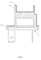
- the isolating composite material 3 may be arranged at one side surface of the second half portion 12 corresponding to the receiving chamber 13.
- the isolating composite material 3 is used for isolating the contact between the second half portion 12 and the detenting assembly 2.
- the above mentioned embodiment is the main skill feature of this invention and corresponds to the claim 1 of this invention to understand the objective and embodiments of this invention in detail.
- the skill features of the depending claims are for describing the claim 1 in detail or adding more skill features, but not limited thereto. It should be known that the claim 1 is not necessary to include the skill features of the depending claims.
- a general electronic switch element is mainly used for controlling the circuit to become the open loop or the closed loop, such as a starter.
- the electronic switch elements which include a switch for operation by hand, a keypad with many buttons or keys, a relay which is for switching the current and an electro-magnetic element but different from the solid-state relay, a contactor, a thermostat for automatically adjusting temperature, a circuit breaker for automatically opening the overcurrent, a limit switch for mechanically activating, a mercury switch, a centrifugal switch, and a connector.
- the above mentioned electronic switch elements are frequently used in the precision instruments.
- the common characteristic of the electronic switch elements is having a plastic housing. It is easy to be sparkled while the inside current is generated and then two ends thereof are separated.
- the sparkle has the instantaneous high temperature which may result in the plastic housing with low melting point being melted and burned and further result in fire. Therefore, the arrangement of the isolating composite material 3 may isolate the detenting assembly 2 which may sparkle and the first and second half portions 11, 12 with low melting point. Thus, the sparkles may not contact the first half portion 11 and the second half portion 12 and the disasters may not happen.
- the isolating composite material 3 may be a ceramic sheet.
- the ceramic material has the characteristics which include anticorrosion, high temperature resistance, wear resistance, light weight, electrics, magnetics, light, and heat. Therefore, the sparkles may be isolated the ceramic sheet from the second half portion 12 to prevent from damage and dangers.
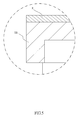
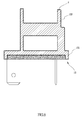
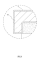
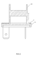
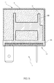
- the isolating composite material 3 with the type of the ceramic sheet is arranged at the side surface of the second half portion 12 which is corresponding to the receiving chamber 13 for easy replacement and may ensure to isolate the second half portion 12 from the influence of the sparkles (shown as in FIGs. 2 , 3 , 6 , 10 , and 11 ).
- the isolating composite material 3 may be a ceramic powder which may be coated on the outer surface of the second half portion 12 (shown as in FIGs. 7 to 9 ).
- the isolating composite material 3 arranged at the second half portion 12 is a form of a cap to cover the bottom plate 12 and a surface of each vertical plate 122 so as to prevent the contact between the detenting assembly 2 and the second half portion 12 and achieve the effect of decreasing the influence of the sparkles (the covering type of the isolating composite material 3 is changeable according to the types of the bottom plate 121 and the vertical plates 122).
- the isolating composite material 3 is not covered on the vertical plates 122. There are two elongated holes 31 which are formed on the isolating composite material 3 with the form of the cap.
- the vertical plates 122 may be passing through the two elongated holes 31 of the isolating composite material 3 so that the isolating composite material 3 may be adhered to the surface of the bottom plate 121.
- the isolating composite material 3 is coated on the all surfaces of the bottom plate 121 and the vertical plates 122 so as to ensure to isolate the detenting assembly 2 from the bottom plate 121 and the vertical plates 122.
- the main objective of above mentioned three embodiments is to isolate the second half portion 12 made by a plastic material from the detenting assembly 2 and prevent from sparkling, burning, and melting.
- the type of being covered the second half portion 12 by the isolating composite material 3 is not limited thereto. Besides, the part of the second half portion 12 corresponding to the detenting assembly 2 which is easiest to be sparkled may be covered or coated to protect.
- the difference between the fourth embodiment and above mentioned three embodiments is that the isolating composite material 3 is arranged at one side surface of the first half portion 11 which is corresponding to the receiving chamber 13. Besides, it may combine the fourth embodiment and the above mentioned three embodiments so that the isolating composite material 3 may be arranged at an inner surface of the first half portion 11 and one side surface of the second half portion 12 corresponding to the receiving chamber 13 or all surfaces of the second half portion 12. Therefore, the protection for the electronic switch elements may be further enhanced and improved.
- the detenting assembly 2 may further include a magnetic coil portion 21 and an electrically conductive metal portion 22.
- the magnetic coil portion 21 is arranged between the two vertical plates 122 of the second half portion 12.
- the electrically conductive metal portion 22 has a metal flat sheet 221 and a metal lock sheet 222,
- the metal flat sheet 221 is arranged at a top end of each vertical plate 122, and the metal lock sheet 222 is arranged at outside of one of the two vertical plates 122.
- One end of the metal lock sheet 222 is assembled with the metal flat sheet 221 and the other end thereof is connected to the outside of the vertical plate 122 (shown as in FIG. 1 ).
- the relay illustrated by FIG. 1 shows one of the preferable embodiments.
- the example of the arrangement of the magnetic coil portion 21 and the electrically conductive metal portion 22 is the inner elements of a specific known relay, but not limited to whole type of relays.
- the isolating composite material 3 may be also used to other electronic switch elements which may generates sparkles to result in burning, but not only limited to the relays.
- the arrangement of the isolating composite material 3 which is cooperated with the characteristic of ceramics is able to isolate the sparkles from the first half portion 11 and the second half portion 12. Thus, the risk of the disasters may be reduced. And compared to the conventional electronic elements, the detenting assembly 2 arranged in the electronic switch elements and the use of the whole electronic switch elements may be protected and have better safety and usefulness.
Landscapes
- Physics & Mathematics (AREA)
- Electromagnetism (AREA)
- Switch Cases, Indication, And Locking (AREA)
Priority Applications (2)
| Application Number | Priority Date | Filing Date | Title |
|---|---|---|---|
| ES15180837T ES2777499T3 (es) | 2015-08-12 | 2015-08-12 | Dispositivo de conmutación electrónico con materiales cerámicos |
| EP15180837.5A EP3131111B1 (de) | 2015-08-12 | 2015-08-12 | Elektronische schaltvorrichtung mit keramischen materialien |
Applications Claiming Priority (1)
| Application Number | Priority Date | Filing Date | Title |
|---|---|---|---|
| EP15180837.5A EP3131111B1 (de) | 2015-08-12 | 2015-08-12 | Elektronische schaltvorrichtung mit keramischen materialien |
Publications (2)
| Publication Number | Publication Date |
|---|---|
| EP3131111A1 true EP3131111A1 (de) | 2017-02-15 |
| EP3131111B1 EP3131111B1 (de) | 2019-12-25 |
Family
ID=53835350
Family Applications (1)
| Application Number | Title | Priority Date | Filing Date |
|---|---|---|---|
| EP15180837.5A Active EP3131111B1 (de) | 2015-08-12 | 2015-08-12 | Elektronische schaltvorrichtung mit keramischen materialien |
Country Status (2)
| Country | Link |
|---|---|
| EP (1) | EP3131111B1 (de) |
| ES (1) | ES2777499T3 (de) |
Citations (4)
| Publication number | Priority date | Publication date | Assignee | Title |
|---|---|---|---|---|
| GB2302989A (en) * | 1995-06-30 | 1997-02-05 | Copal Electronics | Electromagnetic relay |
| EP0798752A2 (de) * | 1996-03-26 | 1997-10-01 | Matsushita Electric Works, Ltd. | Gekapselte Kontaktanordnung mit justierbarem Kontaktabstand |
| US6078491A (en) * | 1996-05-07 | 2000-06-20 | Siemens Aktiengesellschaft | Hybrid relay |
| CN104553181A (zh) * | 2013-10-21 | 2015-04-29 | 丹阳市米可汽车零部件厂 | 复合材料继电器外壳及其制备方法 |
-
2015
- 2015-08-12 ES ES15180837T patent/ES2777499T3/es active Active
- 2015-08-12 EP EP15180837.5A patent/EP3131111B1/de active Active
Patent Citations (4)
| Publication number | Priority date | Publication date | Assignee | Title |
|---|---|---|---|---|
| GB2302989A (en) * | 1995-06-30 | 1997-02-05 | Copal Electronics | Electromagnetic relay |
| EP0798752A2 (de) * | 1996-03-26 | 1997-10-01 | Matsushita Electric Works, Ltd. | Gekapselte Kontaktanordnung mit justierbarem Kontaktabstand |
| US6078491A (en) * | 1996-05-07 | 2000-06-20 | Siemens Aktiengesellschaft | Hybrid relay |
| CN104553181A (zh) * | 2013-10-21 | 2015-04-29 | 丹阳市米可汽车零部件厂 | 复合材料继电器外壳及其制备方法 |
Also Published As
| Publication number | Publication date |
|---|---|
| ES2777499T3 (es) | 2020-08-05 |
| EP3131111B1 (de) | 2019-12-25 |
Similar Documents
| Publication | Publication Date | Title |
|---|---|---|
| US10014098B2 (en) | Surge protection device, comprising at least one surge arrester and one short-circuit switching device which is connected in parallel with the surge arrester, can be thermally tripped and is spring-pretensioned | |
| US20170032917A1 (en) | Electronic switch device with ceramic materials | |
| KR101207581B1 (ko) | 과전류 차단 기능을 갖는 반복형 퓨즈 | |
| KR101401141B1 (ko) | 비정상상태의 전류 및 전압을 차단하는 복합보호소자 | |
| DK2561519T3 (en) | SURGE PROTECTION ELEMENT | |
| US20100219929A1 (en) | Thermal fuse with current fuse function | |
| CN103518240A (zh) | 包括至少一个过压放电器的过压保护装置 | |
| US11417483B2 (en) | Power contactor and method for producing a housing body for the power contactor | |
| TW201421520A (zh) | 阻止電流及電壓異常狀態的複合保護裝置 | |
| CA2898506A1 (en) | Medium voltage controllable fuse | |
| US8294540B2 (en) | Relay with multiple contacts | |
| KR101220283B1 (ko) | 대전류용 반복형 퓨즈 | |
| CN104882342A (zh) | 复合保护装置 | |
| US9564718B2 (en) | Power plug and power receptacle with over-temperature protection function | |
| TWI854976B (zh) | 熱保護裝置 | |
| US9147510B2 (en) | Overvoltage protection element | |
| EP3131111B1 (de) | Elektronische schaltvorrichtung mit keramischen materialien | |
| CN101536130B (zh) | 连接套及配有连接套的开关 | |
| CN1998117B (zh) | 自动解除的过压放电装置及这种过压放电装置的应用 | |
| KR20170124482A (ko) | 세라믹 물질들을 가지는 릴레이 스위치 장치 | |
| KR20170019064A (ko) | 세라믹 물질들을 가지는 릴레이 스위치 장치 | |
| US11208978B1 (en) | Ignition interrupter and related methods | |
| KR20060050897A (ko) | 보호부품, 보호장치, 전지 팩 및 휴대용 전자기기 | |
| TW201421521A (zh) | 阻止電流及電壓異常狀態的複合保護裝置 | |
| JP6594697B2 (ja) | セラミック複合材料を有ずる電子スイッチ部材 |
Legal Events
| Date | Code | Title | Description |
|---|---|---|---|
| PUAI | Public reference made under article 153(3) epc to a published international application that has entered the european phase |
Free format text: ORIGINAL CODE: 0009012 |
|
| STAA | Information on the status of an ep patent application or granted ep patent |
Free format text: STATUS: REQUEST FOR EXAMINATION WAS MADE |
|
| 17P | Request for examination filed |
Effective date: 20160331 |
|
| AK | Designated contracting states |
Kind code of ref document: A1 Designated state(s): AL AT BE BG CH CY CZ DE DK EE ES FI FR GB GR HR HU IE IS IT LI LT LU LV MC MK MT NL NO PL PT RO RS SE SI SK SM TR |
|
| AX | Request for extension of the european patent |
Extension state: BA ME |
|
| GRAP | Despatch of communication of intention to grant a patent |
Free format text: ORIGINAL CODE: EPIDOSNIGR1 |
|
| STAA | Information on the status of an ep patent application or granted ep patent |
Free format text: STATUS: GRANT OF PATENT IS INTENDED |
|
| INTG | Intention to grant announced |
Effective date: 20190717 |
|
| RIN1 | Information on inventor provided before grant (corrected) |
Inventor name: WU, SUNG-JEN |
|
| GRAS | Grant fee paid |
Free format text: ORIGINAL CODE: EPIDOSNIGR3 |
|
| GRAA | (expected) grant |
Free format text: ORIGINAL CODE: 0009210 |
|
| STAA | Information on the status of an ep patent application or granted ep patent |
Free format text: STATUS: THE PATENT HAS BEEN GRANTED |
|
| AK | Designated contracting states |
Kind code of ref document: B1 Designated state(s): AL AT BE BG CH CY CZ DE DK EE ES FI FR GB GR HR HU IE IS IT LI LT LU LV MC MK MT NL NO PL PT RO RS SE SI SK SM TR |
|
| REG | Reference to a national code |
Ref country code: GB Ref legal event code: FG4D |
|
| REG | Reference to a national code |
Ref country code: CH Ref legal event code: EP |
|
| REG | Reference to a national code |
Ref country code: DE Ref legal event code: R096 Ref document number: 602015044166 Country of ref document: DE |
|
| REG | Reference to a national code |
Ref country code: AT Ref legal event code: REF Ref document number: 1218044 Country of ref document: AT Kind code of ref document: T Effective date: 20200115 |
|
| REG | Reference to a national code |
Ref country code: IE Ref legal event code: FG4D |
|
| REG | Reference to a national code |
Ref country code: NL Ref legal event code: MP Effective date: 20191225 |
|
| PG25 | Lapsed in a contracting state [announced via postgrant information from national office to epo] |
Ref country code: SE Free format text: LAPSE BECAUSE OF FAILURE TO SUBMIT A TRANSLATION OF THE DESCRIPTION OR TO PAY THE FEE WITHIN THE PRESCRIBED TIME-LIMIT Effective date: 20191225 Ref country code: LV Free format text: LAPSE BECAUSE OF FAILURE TO SUBMIT A TRANSLATION OF THE DESCRIPTION OR TO PAY THE FEE WITHIN THE PRESCRIBED TIME-LIMIT Effective date: 20191225 Ref country code: GR Free format text: LAPSE BECAUSE OF FAILURE TO SUBMIT A TRANSLATION OF THE DESCRIPTION OR TO PAY THE FEE WITHIN THE PRESCRIBED TIME-LIMIT Effective date: 20200326 Ref country code: BG Free format text: LAPSE BECAUSE OF FAILURE TO SUBMIT A TRANSLATION OF THE DESCRIPTION OR TO PAY THE FEE WITHIN THE PRESCRIBED TIME-LIMIT Effective date: 20200325 Ref country code: NO Free format text: LAPSE BECAUSE OF FAILURE TO SUBMIT A TRANSLATION OF THE DESCRIPTION OR TO PAY THE FEE WITHIN THE PRESCRIBED TIME-LIMIT Effective date: 20200325 Ref country code: FI Free format text: LAPSE BECAUSE OF FAILURE TO SUBMIT A TRANSLATION OF THE DESCRIPTION OR TO PAY THE FEE WITHIN THE PRESCRIBED TIME-LIMIT Effective date: 20191225 Ref country code: LT Free format text: LAPSE BECAUSE OF FAILURE TO SUBMIT A TRANSLATION OF THE DESCRIPTION OR TO PAY THE FEE WITHIN THE PRESCRIBED TIME-LIMIT Effective date: 20191225 |
|
| REG | Reference to a national code |
Ref country code: LT Ref legal event code: MG4D |
|
| PG25 | Lapsed in a contracting state [announced via postgrant information from national office to epo] |
Ref country code: RS Free format text: LAPSE BECAUSE OF FAILURE TO SUBMIT A TRANSLATION OF THE DESCRIPTION OR TO PAY THE FEE WITHIN THE PRESCRIBED TIME-LIMIT Effective date: 20191225 Ref country code: HR Free format text: LAPSE BECAUSE OF FAILURE TO SUBMIT A TRANSLATION OF THE DESCRIPTION OR TO PAY THE FEE WITHIN THE PRESCRIBED TIME-LIMIT Effective date: 20191225 |
|
| PG25 | Lapsed in a contracting state [announced via postgrant information from national office to epo] |
Ref country code: AL Free format text: LAPSE BECAUSE OF FAILURE TO SUBMIT A TRANSLATION OF THE DESCRIPTION OR TO PAY THE FEE WITHIN THE PRESCRIBED TIME-LIMIT Effective date: 20191225 |
|
| REG | Reference to a national code |
Ref country code: DE Ref legal event code: R082 Ref document number: 602015044166 Country of ref document: DE Representative=s name: HELLMICH, WOLFGANG, DE |
|
| PG25 | Lapsed in a contracting state [announced via postgrant information from national office to epo] |
Ref country code: RO Free format text: LAPSE BECAUSE OF FAILURE TO SUBMIT A TRANSLATION OF THE DESCRIPTION OR TO PAY THE FEE WITHIN THE PRESCRIBED TIME-LIMIT Effective date: 20191225 Ref country code: EE Free format text: LAPSE BECAUSE OF FAILURE TO SUBMIT A TRANSLATION OF THE DESCRIPTION OR TO PAY THE FEE WITHIN THE PRESCRIBED TIME-LIMIT Effective date: 20191225 Ref country code: NL Free format text: LAPSE BECAUSE OF FAILURE TO SUBMIT A TRANSLATION OF THE DESCRIPTION OR TO PAY THE FEE WITHIN THE PRESCRIBED TIME-LIMIT Effective date: 20191225 Ref country code: CZ Free format text: LAPSE BECAUSE OF FAILURE TO SUBMIT A TRANSLATION OF THE DESCRIPTION OR TO PAY THE FEE WITHIN THE PRESCRIBED TIME-LIMIT Effective date: 20191225 Ref country code: PT Free format text: LAPSE BECAUSE OF FAILURE TO SUBMIT A TRANSLATION OF THE DESCRIPTION OR TO PAY THE FEE WITHIN THE PRESCRIBED TIME-LIMIT Effective date: 20200520 |
|
| REG | Reference to a national code |
Ref country code: ES Ref legal event code: FG2A Ref document number: 2777499 Country of ref document: ES Kind code of ref document: T3 Effective date: 20200805 |
|
| PG25 | Lapsed in a contracting state [announced via postgrant information from national office to epo] |
Ref country code: SM Free format text: LAPSE BECAUSE OF FAILURE TO SUBMIT A TRANSLATION OF THE DESCRIPTION OR TO PAY THE FEE WITHIN THE PRESCRIBED TIME-LIMIT Effective date: 20191225 Ref country code: SK Free format text: LAPSE BECAUSE OF FAILURE TO SUBMIT A TRANSLATION OF THE DESCRIPTION OR TO PAY THE FEE WITHIN THE PRESCRIBED TIME-LIMIT Effective date: 20191225 Ref country code: IS Free format text: LAPSE BECAUSE OF FAILURE TO SUBMIT A TRANSLATION OF THE DESCRIPTION OR TO PAY THE FEE WITHIN THE PRESCRIBED TIME-LIMIT Effective date: 20200425 |
|
| REG | Reference to a national code |
Ref country code: DE Ref legal event code: R097 Ref document number: 602015044166 Country of ref document: DE |
|
| PG25 | Lapsed in a contracting state [announced via postgrant information from national office to epo] |
Ref country code: DK Free format text: LAPSE BECAUSE OF FAILURE TO SUBMIT A TRANSLATION OF THE DESCRIPTION OR TO PAY THE FEE WITHIN THE PRESCRIBED TIME-LIMIT Effective date: 20191225 |
|
| PLBE | No opposition filed within time limit |
Free format text: ORIGINAL CODE: 0009261 |
|
| STAA | Information on the status of an ep patent application or granted ep patent |
Free format text: STATUS: NO OPPOSITION FILED WITHIN TIME LIMIT |
|
| REG | Reference to a national code |
Ref country code: AT Ref legal event code: MK05 Ref document number: 1218044 Country of ref document: AT Kind code of ref document: T Effective date: 20191225 |
|
| PG25 | Lapsed in a contracting state [announced via postgrant information from national office to epo] |
Ref country code: SI Free format text: LAPSE BECAUSE OF FAILURE TO SUBMIT A TRANSLATION OF THE DESCRIPTION OR TO PAY THE FEE WITHIN THE PRESCRIBED TIME-LIMIT Effective date: 20191225 |
|
| 26N | No opposition filed |
Effective date: 20200928 |
|
| PG25 | Lapsed in a contracting state [announced via postgrant information from national office to epo] |
Ref country code: AT Free format text: LAPSE BECAUSE OF FAILURE TO SUBMIT A TRANSLATION OF THE DESCRIPTION OR TO PAY THE FEE WITHIN THE PRESCRIBED TIME-LIMIT Effective date: 20191225 |
|
| PG25 | Lapsed in a contracting state [announced via postgrant information from national office to epo] |
Ref country code: PL Free format text: LAPSE BECAUSE OF FAILURE TO SUBMIT A TRANSLATION OF THE DESCRIPTION OR TO PAY THE FEE WITHIN THE PRESCRIBED TIME-LIMIT Effective date: 20191225 |
|
| PG25 | Lapsed in a contracting state [announced via postgrant information from national office to epo] |
Ref country code: MC Free format text: LAPSE BECAUSE OF FAILURE TO SUBMIT A TRANSLATION OF THE DESCRIPTION OR TO PAY THE FEE WITHIN THE PRESCRIBED TIME-LIMIT Effective date: 20191225 |
|
| REG | Reference to a national code |
Ref country code: CH Ref legal event code: PL |
|
| GBPC | Gb: european patent ceased through non-payment of renewal fee |
Effective date: 20200812 |
|
| PG25 | Lapsed in a contracting state [announced via postgrant information from national office to epo] |
Ref country code: LU Free format text: LAPSE BECAUSE OF NON-PAYMENT OF DUE FEES Effective date: 20200812 Ref country code: LI Free format text: LAPSE BECAUSE OF NON-PAYMENT OF DUE FEES Effective date: 20200831 Ref country code: CH Free format text: LAPSE BECAUSE OF NON-PAYMENT OF DUE FEES Effective date: 20200831 |
|
| REG | Reference to a national code |
Ref country code: BE Ref legal event code: MM Effective date: 20200831 |
|
| PG25 | Lapsed in a contracting state [announced via postgrant information from national office to epo] |
Ref country code: FR Free format text: LAPSE BECAUSE OF NON-PAYMENT OF DUE FEES Effective date: 20200831 |
|
| PG25 | Lapsed in a contracting state [announced via postgrant information from national office to epo] |
Ref country code: BE Free format text: LAPSE BECAUSE OF NON-PAYMENT OF DUE FEES Effective date: 20200831 Ref country code: GB Free format text: LAPSE BECAUSE OF NON-PAYMENT OF DUE FEES Effective date: 20200812 Ref country code: IE Free format text: LAPSE BECAUSE OF NON-PAYMENT OF DUE FEES Effective date: 20200812 |
|
| PG25 | Lapsed in a contracting state [announced via postgrant information from national office to epo] |
Ref country code: TR Free format text: LAPSE BECAUSE OF FAILURE TO SUBMIT A TRANSLATION OF THE DESCRIPTION OR TO PAY THE FEE WITHIN THE PRESCRIBED TIME-LIMIT Effective date: 20191225 Ref country code: MT Free format text: LAPSE BECAUSE OF FAILURE TO SUBMIT A TRANSLATION OF THE DESCRIPTION OR TO PAY THE FEE WITHIN THE PRESCRIBED TIME-LIMIT Effective date: 20191225 Ref country code: CY Free format text: LAPSE BECAUSE OF FAILURE TO SUBMIT A TRANSLATION OF THE DESCRIPTION OR TO PAY THE FEE WITHIN THE PRESCRIBED TIME-LIMIT Effective date: 20191225 |
|
| PG25 | Lapsed in a contracting state [announced via postgrant information from national office to epo] |
Ref country code: MK Free format text: LAPSE BECAUSE OF FAILURE TO SUBMIT A TRANSLATION OF THE DESCRIPTION OR TO PAY THE FEE WITHIN THE PRESCRIBED TIME-LIMIT Effective date: 20191225 |
|
| PGFP | Annual fee paid to national office [announced via postgrant information from national office to epo] |
Ref country code: ES Payment date: 20250908 Year of fee payment: 11 |
|
| PGFP | Annual fee paid to national office [announced via postgrant information from national office to epo] |
Ref country code: DE Payment date: 20250624 Year of fee payment: 11 |
|
| PGFP | Annual fee paid to national office [announced via postgrant information from national office to epo] |
Ref country code: IT Payment date: 20250626 Year of fee payment: 11 |