EP3131124B1 - Photodétecteur infrarouge basé sur une diode à effet tunnel résonant - Google Patents
Photodétecteur infrarouge basé sur une diode à effet tunnel résonant Download PDFInfo
- Publication number
- EP3131124B1 EP3131124B1 EP15181128.8A EP15181128A EP3131124B1 EP 3131124 B1 EP3131124 B1 EP 3131124B1 EP 15181128 A EP15181128 A EP 15181128A EP 3131124 B1 EP3131124 B1 EP 3131124B1
- Authority
- EP
- European Patent Office
- Prior art keywords
- layer
- barrier
- layer structure
- photodetector
- barrier layer
- Prior art date
- Legal status (The legal status is an assumption and is not a legal conclusion. Google has not performed a legal analysis and makes no representation as to the accuracy of the status listed.)
- Active
Links
- 230000005641 tunneling Effects 0.000 title claims description 75
- 230000004888 barrier function Effects 0.000 claims description 137
- 238000010521 absorption reaction Methods 0.000 claims description 68
- 229910005542 GaSb Inorganic materials 0.000 claims description 49
- 239000000463 material Substances 0.000 claims description 31
- 230000008859 change Effects 0.000 claims description 21
- 239000000758 substrate Substances 0.000 claims description 20
- 238000001514 detection method Methods 0.000 claims description 19
- 238000000034 method Methods 0.000 claims description 13
- 229910001218 Gallium arsenide Inorganic materials 0.000 claims description 12
- 238000007789 sealing Methods 0.000 claims description 10
- 239000004065 semiconductor Substances 0.000 claims description 8
- 150000001875 compounds Chemical class 0.000 claims description 5
- 229910000673 Indium arsenide Inorganic materials 0.000 claims 3
- RPQDHPTXJYYUPQ-UHFFFAOYSA-N indium arsenide Chemical compound [In]#[As] RPQDHPTXJYYUPQ-UHFFFAOYSA-N 0.000 claims 3
- 239000010410 layer Substances 0.000 description 291
- 238000010586 diagram Methods 0.000 description 13
- 238000005286 illumination Methods 0.000 description 10
- 230000035945 sensitivity Effects 0.000 description 10
- 230000003321 amplification Effects 0.000 description 9
- 230000008901 benefit Effects 0.000 description 9
- 238000003199 nucleic acid amplification method Methods 0.000 description 9
- 229910000661 Mercury cadmium telluride Inorganic materials 0.000 description 5
- 230000007547 defect Effects 0.000 description 5
- 230000008569 process Effects 0.000 description 5
- 230000005428 wave function Effects 0.000 description 5
- 230000007423 decrease Effects 0.000 description 4
- 238000005421 electrostatic potential Methods 0.000 description 4
- 239000008393 encapsulating agent Substances 0.000 description 4
- 229910017115 AlSb Inorganic materials 0.000 description 3
- 239000002800 charge carrier Substances 0.000 description 3
- 238000001816 cooling Methods 0.000 description 3
- 230000003993 interaction Effects 0.000 description 3
- 230000007704 transition Effects 0.000 description 3
- VYPSYNLAJGMNEJ-UHFFFAOYSA-N Silicium dioxide Chemical compound O=[Si]=O VYPSYNLAJGMNEJ-UHFFFAOYSA-N 0.000 description 2
- 230000003247 decreasing effect Effects 0.000 description 2
- 238000005530 etching Methods 0.000 description 2
- 238000005259 measurement Methods 0.000 description 2
- 230000003287 optical effect Effects 0.000 description 2
- 239000002245 particle Substances 0.000 description 2
- 238000011896 sensitive detection Methods 0.000 description 2
- 238000000926 separation method Methods 0.000 description 2
- 229910000530 Gallium indium arsenide Inorganic materials 0.000 description 1
- 229910052581 Si3N4 Inorganic materials 0.000 description 1
- 206010000210 abortion Diseases 0.000 description 1
- 231100000176 abortion Toxicity 0.000 description 1
- UMIVXZPTRXBADB-UHFFFAOYSA-N benzocyclobutene Chemical compound C1=CC=C2CCC2=C1 UMIVXZPTRXBADB-UHFFFAOYSA-N 0.000 description 1
- 230000015572 biosynthetic process Effects 0.000 description 1
- 229910052681 coesite Inorganic materials 0.000 description 1
- 229910052906 cristobalite Inorganic materials 0.000 description 1
- 230000001419 dependent effect Effects 0.000 description 1
- 239000002019 doping agent Substances 0.000 description 1
- 238000001312 dry etching Methods 0.000 description 1
- 230000000694 effects Effects 0.000 description 1
- 238000010893 electron trap Methods 0.000 description 1
- 238000005516 engineering process Methods 0.000 description 1
- 238000010438 heat treatment Methods 0.000 description 1
- 230000010354 integration Effects 0.000 description 1
- 230000007246 mechanism Effects 0.000 description 1
- 230000003647 oxidation Effects 0.000 description 1
- 238000007254 oxidation reaction Methods 0.000 description 1
- 230000001590 oxidative effect Effects 0.000 description 1
- 230000035699 permeability Effects 0.000 description 1
- 231100000614 poison Toxicity 0.000 description 1
- 230000007096 poisonous effect Effects 0.000 description 1
- 229920000642 polymer Polymers 0.000 description 1
- 239000000377 silicon dioxide Substances 0.000 description 1
- 239000002356 single layer Substances 0.000 description 1
- 230000007480 spreading Effects 0.000 description 1
- 229910052682 stishovite Inorganic materials 0.000 description 1
- 239000000126 substance Substances 0.000 description 1
- 229910052905 tridymite Inorganic materials 0.000 description 1
- 238000001039 wet etching Methods 0.000 description 1
Images





Classifications
-
- H—ELECTRICITY
- H10—SEMICONDUCTOR DEVICES; ELECTRIC SOLID-STATE DEVICES NOT OTHERWISE PROVIDED FOR
- H10F—INORGANIC SEMICONDUCTOR DEVICES SENSITIVE TO INFRARED RADIATION, LIGHT, ELECTROMAGNETIC RADIATION OF SHORTER WAVELENGTH OR CORPUSCULAR RADIATION
- H10F30/00—Individual radiation-sensitive semiconductor devices in which radiation controls the flow of current through the devices, e.g. photodetectors
- H10F30/20—Individual radiation-sensitive semiconductor devices in which radiation controls the flow of current through the devices, e.g. photodetectors the devices having potential barriers, e.g. phototransistors
- H10F30/21—Individual radiation-sensitive semiconductor devices in which radiation controls the flow of current through the devices, e.g. photodetectors the devices having potential barriers, e.g. phototransistors the devices being sensitive to infrared, visible or ultraviolet radiation
- H10F30/22—Individual radiation-sensitive semiconductor devices in which radiation controls the flow of current through the devices, e.g. photodetectors the devices having potential barriers, e.g. phototransistors the devices being sensitive to infrared, visible or ultraviolet radiation the devices having only one potential barrier, e.g. photodiodes
-
- H—ELECTRICITY
- H10—SEMICONDUCTOR DEVICES; ELECTRIC SOLID-STATE DEVICES NOT OTHERWISE PROVIDED FOR
- H10F—INORGANIC SEMICONDUCTOR DEVICES SENSITIVE TO INFRARED RADIATION, LIGHT, ELECTROMAGNETIC RADIATION OF SHORTER WAVELENGTH OR CORPUSCULAR RADIATION
- H10F77/00—Constructional details of devices covered by this subclass
- H10F77/10—Semiconductor bodies
- H10F77/12—Active materials
- H10F77/124—Active materials comprising only Group III-V materials, e.g. GaAs
- H10F77/1248—Active materials comprising only Group III-V materials, e.g. GaAs having three or more elements, e.g. GaAlAs, InGaAs or InGaAsP
-
- H—ELECTRICITY
- H10—SEMICONDUCTOR DEVICES; ELECTRIC SOLID-STATE DEVICES NOT OTHERWISE PROVIDED FOR
- H10F—INORGANIC SEMICONDUCTOR DEVICES SENSITIVE TO INFRARED RADIATION, LIGHT, ELECTROMAGNETIC RADIATION OF SHORTER WAVELENGTH OR CORPUSCULAR RADIATION
- H10F77/00—Constructional details of devices covered by this subclass
- H10F77/10—Semiconductor bodies
- H10F77/14—Shape of semiconductor bodies; Shapes, relative sizes or dispositions of semiconductor regions within semiconductor bodies
- H10F77/143—Shape of semiconductor bodies; Shapes, relative sizes or dispositions of semiconductor regions within semiconductor bodies comprising quantum structures
-
- H—ELECTRICITY
- H10—SEMICONDUCTOR DEVICES; ELECTRIC SOLID-STATE DEVICES NOT OTHERWISE PROVIDED FOR
- H10F—INORGANIC SEMICONDUCTOR DEVICES SENSITIVE TO INFRARED RADIATION, LIGHT, ELECTROMAGNETIC RADIATION OF SHORTER WAVELENGTH OR CORPUSCULAR RADIATION
- H10F77/00—Constructional details of devices covered by this subclass
- H10F77/10—Semiconductor bodies
- H10F77/14—Shape of semiconductor bodies; Shapes, relative sizes or dispositions of semiconductor regions within semiconductor bodies
- H10F77/146—Superlattices; Multiple quantum well structures
-
- H—ELECTRICITY
- H10—SEMICONDUCTOR DEVICES; ELECTRIC SOLID-STATE DEVICES NOT OTHERWISE PROVIDED FOR
- H10F—INORGANIC SEMICONDUCTOR DEVICES SENSITIVE TO INFRARED RADIATION, LIGHT, ELECTROMAGNETIC RADIATION OF SHORTER WAVELENGTH OR CORPUSCULAR RADIATION
- H10F77/00—Constructional details of devices covered by this subclass
- H10F77/10—Semiconductor bodies
- H10F77/14—Shape of semiconductor bodies; Shapes, relative sizes or dispositions of semiconductor regions within semiconductor bodies
- H10F77/147—Shapes of bodies
-
- H—ELECTRICITY
- H10—SEMICONDUCTOR DEVICES; ELECTRIC SOLID-STATE DEVICES NOT OTHERWISE PROVIDED FOR
- H10F—INORGANIC SEMICONDUCTOR DEVICES SENSITIVE TO INFRARED RADIATION, LIGHT, ELECTROMAGNETIC RADIATION OF SHORTER WAVELENGTH OR CORPUSCULAR RADIATION
- H10F77/00—Constructional details of devices covered by this subclass
- H10F77/20—Electrodes
- H10F77/206—Electrodes for devices having potential barriers
- H10F77/241—Electrodes for devices having potential barriers comprising ring electrodes
Definitions
- the present invention is related to photodetection and belongs to the field of semiconductor photodetectors.
- Photodetectors based on HgCdTe allow for photodetection in a range between 1 ⁇ m to 30 ⁇ m.
- HgCdTe is highly poisonous. Since HgCdTe is not RoHS compliant, its use is widely prohibited. Further, HgCdTe structures exhibit a low uniformity due to a low vapor pressure of Hg. Therefore, photodetectors based on HgCdTe suffer from a low yield due to defects and leaking currents.
- photodetectors which are sufficiently sensitive.
- amplifiers are used, which may also be integrated into the photodetectors.
- photodetectors with internal amplification are resonant tunneling diodes (RTDs) combined with an absorption layer as well as avalanche-photodiodes (APDs). While APDs usually have an operating voltage between 50 V and 100 V, RTDs have an advantageously low operating voltage below 5 V.
- Photodetectors which combine RTDs and internal absorption layers provide a very efficient amplification and allow for a very sensitive detection. These photodetectors also allow for a fast detection with a high time resolution, however, compared to APD they are less fast. These advantages generally result from the fact that a tunneling current of the RTD reacts very sensitively to photon induced changes in a local electrostatic potential.
- Fig. 1 shows an ideal current voltage characteristic 10 of an RTD and three load lines A, B and C.
- the ideal current voltage characteristic 10 has a local maximum, a local minimum and a NDR region in between where the current decreases if the voltage increases. In the NDR region the ideal current voltage characteristic 10 has a negative differential resistance (NDR).
- NDR negative differential resistance
- Each of the load lines A, B and C corresponds to a different voltage V 1 , V 2 and V 3 which is applied to a circuit comprising the RTD.
- the slope of the load lines corresponds to -1/R, wherein R is the resistance of the circuit comprising the RTD.
- each of the load lines A and C intersects the ideal current voltage characteristic 10 in one point, which respectively corresponds to a stable operating point.
- Load line B has three intersections, wherein only the left intersection and the right intersection correspond to stable operating points.
- the intersection in the NDR region is unstable. Those intersections which correspond to stable operating points indicate at the y-axis the current which will actually flow through the RTD and at the x-axis the actually resulting voltage over the RTD.
- the voltage of a load line, such as V 1 for load line A, and the current of the stable working point of that load line, such as current I 1 for load line A in Fig. 1 form a point (V 1 ; I 1 ) on an actual current voltage characteristic 12 of the RTD, which is illustrated in Fig. 2 .
- the actual current voltage characteristic 12 can be obtained by applying different voltages V to the circuit comprising the RTD and by measuring for each voltage V the corresponding current I flowing through the RTD. In other words, if an external voltage is applied to the circuit comprising the RTD the actual current voltage characteristic 12 indicates the respective current which flows in stable condition.
- the actual current voltage characteristic 12 has a bi-stable region between threshold voltages V t1 and V t2 where two different stable operating conditions exist, because the resistance R is sufficiently large.
- Load lines obtained for voltages within the bi-stable region e.g. load line B in Fig. 1
- Load lines obtained for voltages outside the bi-stable region, e.g. load lines A and C in Fig. 1 have only one intersection with the ideal current voltage characteristic 10. For these load lines there is only one stable working point.
- the above current switching occurring when leaving the bi-stable region can be used for an effective amplification when detecting photons, as will be explained in the following.
- One possibility to induce the current switching is to change the externally applied voltage or to change the resistance within the circuit. Thereby the load line is shifted or rotated in Fig. 1 with respect to the ideal current voltage characteristic 10.
- Another possibility is to shift the ideal current voltage characteristic 10 with respect to the load line. Such a shift can be induced by photon absorption, which will be explained with reference to Fig. 3 .
- Fig. 3 shows the energy of a conduction band 14 and a valence band 16 along a layer structure of an RTD having an integrated absorption layer 26.
- the layer structure of Fig. 3 comprises from left to right an n-doped region 18, a first barrier layer 20, an inter-barrier layer 22, a second barrier layer 24 and the absorption layer 26.
- the layer structure of Fig. 3 is biased by a voltage leading to an energy difference ⁇ E over the barrier layer structure 20, 22 and 24 in the energy bands.
- the inter-barrier layer 22 provides an electron well in the conduction band 14 leading to separated energy states for electrons, as is illustrated by horizontal lines in Fig. 3 .
- the n-doping movable electrons are provided in the conduction band 14 in the n-doped region 18 with an energy determined by the energy of the conduction band 14. If the energy of the movable electrons corresponds to the energy of an energy state between the barrier layers 20, 24, the electrons are not blocked at the barrier layer structure 20, 22 and 24 but can resonantly tunnel through the barrier layer structure 20, 22 and 24. In other words, if the layer structure is biased, such that the electron energy coincides with an energy state in the well the barrier layer structure 20, 22, 24 becomes permeable resulting in a resonant tunneling current.
- the local peaks in the current voltage characteristics 10, 12 of Figs. 1 and 2 correspond to such a resonant tunneling current.
- the resonant tunneling current decreases even though the voltage and therefore the energy difference ⁇ E increases. This is due to an increasing misalignment between the energy of the electrons and the energy state in the inter-barrier layer 22 leading to a reduced permeability of the barriers 20, 24 and therefore to a reduced resonant tunneling current.
- FIG. 4 shows a part of the actual current voltage characteristic 12 of Fig. 1 which is not shifted without illumination (solid line) and which is shifted under illumination (dashed lines).
- the actual current voltage characteristic 12 shown in Fig. 4 has an upper branch comprising one of the abovementioned two stable operating conditions and a lower branch comprising the other stable operating condition. If an alternating voltage, e.g.
- V(t) V 0 + V A ⁇ sin( ⁇ t)
- V t2 V 0 + V A ⁇ sin( ⁇ t)
- the working point can alternate on the upper branch between a lower voltage which is smaller than V t2 and an upper voltage which is larger than V t2 and smaller than V t1 .
- the current through the RTD alternates continuously between a lower current and an upper current without abrupt current changes.
- V t2 and V t1 are shifted to the positions of the dashed lines such that the applied voltage passes both the shifted V t1 and the shifted V t1 .
- the applied voltage passes the shifted V t1 from left to right (i.e.
- the abrupt current changes which are light-induced can be comparatively large and therefore allow for a very efficient amplification when detecting photons.
- the Geigermodus allows for a high amplification, because at the transition between working points a slight photon induced shift of the current voltage characteristic 10 can induce a large current change.
- the position, orientation and variation of the load line can be adjusted, such that only illumination above a predefined threshold is discretely detected, while illumination below the predefined threshold is not detected. In principle it is possible, that the predefined threshold allows for single photon detection. Further, depending on the frequency of the applied alternating voltage the detection can be fast and can have a high time resolution.
- RTDs can also be used for other advantageous types of fast and sensitive photodetection, which use the above explained phenomenon that a tunneling current sensitively reacts to illumination, because photogenerated charge carriers cause changes in a local electrostatic potential.
- RTD photodetectors which offer the above advantages are described in US 2011/0068853 A1 and WO 2009/106595 A1 .
- One of these examples comprises an AlSb/GaSb/AlSb-barrier layer structure formed on a layer of InAs. This structure can be used to detect photons in the wavelength range between 1.8 ⁇ m and 4 ⁇ m.
- Further examples for RTD photodetectors are provided in US 8143648 B1 , US 5446293 and EP 0 706 225 A1 . These photodetectors allow for photodetection in the visible and near infrared region. The detectable photon wavelength depends on the material which is used for the absorption layer 26. If the absorption layer 26 and the RTD are integrally formed they comprise materials which can be grown in a common layer structure. Examples for such layer structures are based on GaAs, InP, InAs substrates.
- the object of the present invention is to provide a photodetector which allows for sensitive detection of photons having a wavelength between 1,7 ⁇ m and 30 ⁇ m, wherein the detection can be performed at comparatively high temperatures.
- a further object is to provide a method for forming a layer structure for a corresponding photodetector.
- the present invention provides a photodetector according to claim 1.
- the photodetector of the present invention comprises a p-doped layer instead of a n-doped layer. Accordingly, the resonant tunneling current is not created by electrons tunneling through the barrier layer structure in the conduction band but can be provided by holes tunneling through the barrier layer structure in the valence band. Unlike in photodetectors of the prior art, the tunneling current is not controlled or changed by accumulated photon-induced holes but by photon-induced electrons which accumulate in the conduction band at the barrier layer structure or within the barrier layer structure.
- the absorption layer and the resonant tunneling structure are integrally formed, i.e. can be comprised in a layer structure comprising layers which are deposited above each other and forming a functional unit, also the absorption layer can be selected from a wider range of materials. This allows using materials which are suitable for photoelectric absorption of photons in a range between 1,7 ⁇ m and 30 ⁇ m and which cannot be used to form layer structures having a NDR region when being n-doped or which can only have a NDR region at lower temperatures when being n-doped.
- the p-doping allows that layer structures of RTD photodetectors having a NDR region can comprise materials absorbing in a range between 1,7 ⁇ m and 30 ⁇ m or that such RTD photodetectors still have the NDR region at higher temperatures. Therefore, the p-doping allows using a NDR region for effective photodetection in a wider range above 1,7 ⁇ m or at least at higher temperatures in a wider range above 1,7 ⁇ m.
- the first p-doped layer can be used to provide holes as free charge carriers, which can resonantly tunnel through the barrier layer structure, if the layer structure is biased accordingly.
- the barrier layer structure can be arranged, for example, between the absorption layer and the first p-doped layer.
- the absorption layer can also be arranged within the barrier layer structure, for example.
- the resonant tunneling structure is unipolar and further comprises a second p-doped layer, wherein the barrier layer structure and the absorption layer are arranged between the first p-doped layer and the second p-doped layer.
- An unipolar resonant tunneling structure is only doped by one doping type, in the present case p-doped, such that the resonant tunneling current is only created by hole conduction but not additionally by electron conduction. If the barrier layer structure is arranged between the first p-doped layer and the second p-doped layer, both of the p-doped layers can be used as contacts or as conductive interfaces to contacts which can be used to apply a voltage over the barrier layer structure.
- the absorption layer comprises GaInAsSb and/or a GaInSb/InAs-superlattice.
- GaInAsSb allows for photon absorption in a range between about 1.7 ⁇ m to about 5 ⁇ m.
- the GaInSb/InAs-superlattice can be formed to allow for a photoelectric absorption in the wavelength range between about 2.5 ⁇ m to about 30 ⁇ m.
- the integrally formed layer structure comprises GaSb and/or ternary, quaternary or quinternary compound semiconductors with a lattice constant between 6.05 ⁇ and 6.15 ⁇ .
- GaSb has a lattice constant of about 6.098 ⁇ .
- layer structures are lattice matched to avoid defects and strain.
- lattice matched layer structures different layers being grown above each other have the same lattice constant.
- a pseudo-morphous growth wherein the difference in the lattice constants of adjacent layers is sufficiently low. Therein, the allowable difference in the lattice constants depends on the layer thickness.
- the layers which are deposited above each other and which exceed a certain thickness need to have a lattice constants sufficiently close to each other.
- Ternary, quaternary and quinternary compound semiconductors with a lattice constant in the above range can be grown with a sufficient thickness on GaSb to form an integral layer structure with a degree of defects and strain which is sufficiently low. Further, such materials can be suitable to be used as barrier layers, absorption layers or other layers in a layer structure comprising GaSb.
- the integrally formed layer structure may be arranged on a substrate comprising GaSb.
- a GaSb substrate can be used as a starting point on which the layer structure comprising the resonant tunneling structure and the absorption layer can be formed or deposited.
- the barrier layers may comprise AlAsSb. This material is suitable to provide barriers for holes in the valence band and barriers for electrons in the conduction band.
- the barrier layer structure comprises an AlAsSb/GaSb/AlAsSb double barrier structure.
- the barrier layer structure may comprise a layer which provides an electron well in the conduction band, wherein the layer is arranged at the barrier layer structure and is arranged between the barrier layer structure and the absorption layer. This allows confining photon generated electrons at or within the barrier structure. Because the barrier layer structure comprises an electron well or electron trap in the conduction band, while providing a hole tunneling barrier in the valence band, photogenerated electrons are locally confined within the hole tunneling barrier. This leads to a maximized Coulomb interaction of the photogenerated electrons, and thus to a maximized shift of the energy state in the inter-barrier layer corresponding to a resonant tunneling energy level. This may lead to a larger current signal.
- the lifetime of the electrons which are accumulated within the barrier layer structure and are used to control or change the resonant tunneling current can be increased.
- the longer the lifetime the longer is the period in which the tunneling current is changed. This may lead to a larger amplification factor. Therefore, the electron well in the conduction band can increase the sensitivity of the photodetector.
- the barrier layer structure may comprise two spatially separated double layers, wherein each double layer may comprise a first layer of a first material (AlAsSb) providing an electron barrier in the conduction band and a first hole barrier in the valence band, and a second layer of a second material (InAs) providing an electron well in the conduction band and a second hole barrier in the valence band.
- AlAsSb first material
- InAs second material
- the electron well in the conduction band can provide the above described advantage of an increased sensitivity.
- the second material can simultaneously modify the double barrier in the valence band for the holes.
- the second hole barrier provided by the second material is higher than the first hole barrier provided by the first material. If the height of the hole barrier is increased, the energy states between the barriers are sharper and less spread leading to a more pronounced resonance in the current voltage characteristic. This can be used to increase the sensitivity of the photodetector.
- a higher barrier for holes further reduces non-resonant hole tunneling through the double barrier leading to a reduced leaking current. Additionally, further non-resonant channels such as thermionic emission are drastically reduced which also leads to an increased sensitivity.
- the barrier layer structure comprises two spatially separated double layers, wherein each double layer comprises a first layer comprising AlAsSb and a second layer comprising InAs.
- AlAsSb can provide a barrier for electrons in the conduction band and a barrier for the holes in the valence band, wherein InAs can provide an electron well in the valence band and can simultaneously increase the barrier height for holes in the valence band.
- At least one of the p-doped layers and the barrier layer structure can be comprised in a mesa structure, wherein the photodetector can further comprise an insulating sealing layer capping the mesa structure. Because of the mesa structure, the resonant tunneling current can be limited to a defined spatial region.
- the sealing layer can protect the layer structure including the resonant tunneling structure and the absorption layer and may prevent, for example, an oxidation and a formation of a conductive oxide or of a metallic film which could compromise the function of the photodetector.
- the sealing layer can be formed, for example, by GaAs or InAs. GaAs does not oxidize when exposed to air and is chemically stable. Further, it is transparent for wavelengths above 900 nm, such that photons to be detected are not prevented from reaching the absorption layer.
- the photodetector can further comprise a voltage or current source for biasing the resonant tunneling structure to provide a tunneling current, wherein the tunneling current is based on hole conduction, and a detection apparatus for detecting a change of the tunneling current, wherein the change is induced by photon absorption.
- the present invention further comprises a method according to claim 13.
- the aforementioned steps of growing can be performed in an order, such that in the layer structure a barrier layer structure, which comprises the first and second barrier layers and the inter-barrier layer is arranged, for example, between the absorption layer and the p-doped layer.
- the steps of growing are performed in an order, such that the absorption layer is arranged within the barrier layer structure.
- the aspect of the present invention of using a p-doping for RTD based photodetectors can also be used in combination with other absorption layers, which can comprise different materials as have been described so far and which can thus be photosensitive in other wavelength regions different from the region between 1,7 ⁇ m and 30 ⁇ m.
- Such other photodetectors may provide similar advantages.
- the inventive concept of using a p-doping for an RTD can also be applied to layer structures with resonant tunneling structures but without integrated absorption layers.
- the present disclosure also comprises layer structures having a p-doping and a resonant tunneling structure but no absorption layer. All embodiments or examples disclosed in this application do still form examples of the present disclosure, when the absorption layer is not present. The effect of the p-doping, namely to have a more pronounced resonance at the same temperature, may still be present without the additional absorption layer.
- Further materials or material systems which are suitable for a p-doping are layer structures which can be grown on InP or GaN or are based on InP or GaN.
- Ternary semiconductor materials which can be integrally formed together with InP are InGaAs, InAlAs, AlAsSb, GaAsSb, for example.
- layer structures of materials or material systems which are grown on a ternary quasi-substrate having a desired adjusted lattice constant are the present invention comprises also these embodiments.
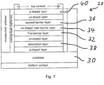
- Fig. 7 shows an RTD 28 according to an embodiment of the present invention.
- the RTD 28 comprises an integrally formed layer structure which is arranged on a substrate 30.
- the layer structure comprises a barrier layer structure formed by a first barrier layer 32, an inter-barrier layer 34 and a second barrier layer 36 and further comprises an absorption layer 38.
- the layer structure further comprises a p-doped layer 40, wherein the barrier layer structure is arranged between the p-doped layer 40 and the absorption layer 38.
- the barrier layer structure 32, 34, 36 creates a double barrier for holes in the valence band and a barrier for electrons in the conduction band.
- the p-doped layer 40 provides holes as free charge carriers which may resonantly tunnel through the barrier layer structure if the RTD 28 is biased with a corresponding voltage. If the RTD 28 is biased for photodetection, photons can be absorbed in the absorption layer 38 leading to the creation of an electron hole pair, wherein the holes move towards the substrate 30 and the electrons move towards the barrier layer structure 32, 34, 36. At the barrier layer structure 32, 34, 36 the electrons are accumulated and induce a change in the resonant tunneling current which is created by the holes provided by the p-doped layer 40.
- the resonant tunneling structure of the RTD 28 is combined with a p-doping. Due to the p-doping the RTD 28 can be both employed with materials selected from a larger variety of materials and can be used for a highly sensitive photodetection above certain temperatures using an amplification mechanism depending on the existence of a NDR region.
- the layer structure of the RTD 28 can be based on GaSb, for example.
- “Based on GaSb” means that the layer structure as functional unit can be integrally formed by sequentially growing layers on a GaSb substrate and/or that GaSb layers can be deposited in the layer structure without necessarily leading to an inoperable layer structure.
- the layer structure is composed of materials having lattice constants which are sufficiently close to the lattice constant of GaSb, such that the layers can be formed or deposited without significant distortions or defects above each other.
- a layer structure based on GaSb may comprise ternary, quaternary and/or quinternary compound semiconductors comprising both Ga and Sb. However, also layers of a material can be included which do not comprise any of Ga and Sb.
- Fig. 8 shows an energy momentum diagram for GaSb on the left and for GaAs on the right.
- the diagrams of Fig. 8 can be used to provide an explanation, why, contrary to common wisdom, it can be advantageous to use a p-doped RTD instead of using an n-doped RTD.
- N-doped RTDs are based on electron conduction, wherein the electrons are transported in the conduction band 14. Within the conduction band 14 there are different stable energy states for electrons in which the electrons have a different k-vector or momentum. Such stable energy states are located at the ⁇ point and at the L point which are indicated in the left diagram of Fig. 8 .
- the energy difference between the L point and the ⁇ point for electrons at 300 K is about 84 meV for GaSb and about 290 meV for GaAs. Because of the lower energy difference, it is more likely for GaSb that electrons move from the ⁇ point to the L point, such that in GaSb the occupation at the L point is higher as compared to GaAs. The additional occupation at the L point leads to a spreading of energy levels in and around the barrier layer structure. As a result the energy states of the system are less discrete and additional channels for tunneling exist. An additional result is an increased interaction with phonons leading to additional tunneling processes. This results in a less pronounced resonance in the current voltage characteristic.
- the occupation at the L point does not only depend on the energy difference between ⁇ point and L point but also on temperature. The higher the temperature, the higher is the electron energy and the higher is the additional occupation at the L point. Because of the lower energy difference for GaSb, at the same temperature the electron occupation at the L point, i.e. number of elections in the illustrated "L-valley", is higher as compared to GaAs.
- GaSb has an occupation at the L point, which for RTDs based on GaSb can lead to a current voltage characteristic without NDR region (as shown in Fig. 6b ), while RTDs based on GaAs can still have a NDR region in the current voltage characteristic at 300 K.
- RTDs based on GaSb may not be suitable for a sensitive photodetection at 300 K, while RTDs based on GaAs may still be suitable at 300 K.
- the inventors have found that the NDR region can be recovered without cooling by using a p-doping instead of using a n-doping without need to change the base material.
- a p-doping instead of using a n-doping without need to change the base material.
- the energetic separation in the conduction band 14 between the L point and the ⁇ point is comparatively small. Therefore, at this temperature electrons occupy the both the ⁇ point and the L point, whereby additional transport channels are opened for electron conduction in the conduction band 14.
- the NDR region disappears or is at least less pronounced in a RTD based on GaSb which is n-doped and which is therefore operated based on electron conduction, i.e.
- an RTD which is p-doped and operated based on hole conduction allows for a similar sensitive photodetection at higher temperatures as compared to the case, when the RTD would be n-doped and operated based on electron conduction.
- n-doped RTDs based on GaSb may not have a NDR region at 300 K, as is illustrated in Fig. 6b , and may therefore not be suitable for sensitive photodetection at 300 K.
- integrally formed layer structures based on GaSb can include a tunneling structure and an absorption layer 38 which together allow for sensitive photodetection in the range between 1,7 ⁇ m and 30 ⁇ m.
- the present invention is not limited to layer structures or RTDs which are based on GaSb but also comprises embodiments with layer structures based on other materials.
- the use of a p-doped RTD which at first view is a disadvantage, can allow for sensitive photodetection at higher temperatures and can allow for sensitive photodetection in a wider wavelength range without need for further cooling.
- Fig. 9 illustrates a process of forming the RTD 28 of Fig. 7 . The process is further illustrated by Figs. 10a - h .
- a substrate 30 is provided, as is illustrated in Fig. 10a .
- the substrate corresponds to a GaSb wafer.
- the wafer may have a thickness of 500 ⁇ m, for example. In other examples the substrate can have a different thickness.
- a layer structure 50 is epitaxially grown on the substrate 30.
- Growing of the layer structure 50 comprises a sequential growing of the following layers on the substrate and above each other in the following sequence starting from the substrate: a p-doped layer 52, the absorption layer 38, an undoped layer 54, the first barrier layer 32, the inter-barrier layer 34, the second barrier layer 36, an undoped layer 56 and the aforementioned p-doped layer 40.
- the p-doped layer 52 can correspond to a p-doped GaSb layer.
- the layer can have a thickness of between 200 nm and 500 nm, for example, and can have a doping concentration of about 10 18 /cm 3 .
- the doping material can be Be, for example.
- the absorption layer 38 can correspond to a layer of GaInAsSb, as will be described further below with respect to Figs. 12a and b , or may correspond to a type-II InAs/GaInSb superlattice. Further, the absorption layer 38 may correspond to a combination of both, as is illustrated in Figs. 14a and 14b .
- the absorption layer 38 can have a thickness of between 10 nm and 5 ⁇ m, for example. If the absorption layer 38 is too thin, only a portion of the photons are absorbed. If the absorption layer 38 is too thick, the number of photogenerated electrons, which recombine and do not accumulate at or in the barrier structure, may be too large.
- the layer 54 can correspond to an undoped GaSb layer having a thickness of between 5 nm and 40 nm, for example.
- the barrier layers 32 and 36 can correspond to layers of AlAsSb. Alternatively, the barrier layers 32 and 36 can correspond in the aforementioned examples to AlSb layers. Each of the barrier layers 32 and 36 can have a thickness of between 1 nm and 10 nm, such as a thickness of about 4 nm, for example. In a further example, each of the barrier layers 32 and 36 consists of an AlAsSb/InAs double layer, as is illustrated in Figs. 13a and b. The AlAsSb layer and the InAs layer in each of the double layers 32 and 36 can have a thickness of about 2 nm, for example.
- the inter-barrier layer 34 may correspond to an undoped GaSb layer of a thickness of between 1 nm and 10 nm, for example of a thickness of about 3 nm.
- the thickness of the inter-barrier layer 34 which provides a quantum well, is adjusted such that the energy states within the barrier structure are sufficiently separated. Because the layer structure 50 is designed for hole conduction and holes have a smaller De Broglie wavelength than electrons, the inter-barrier layer 34 is preferably thinner as compared to layer structures designed for electron conduction. For electron conduction the inter-barrier layers usually has a thickness of between 5 nm and 6 nm.
- the examples described so far have a double barrier structure.
- the barrier layer structure comprises more than two barriers which also allows for resonant tunneling.
- the layer 56 can correspond to an undoped GaSb layer having a thickness of between 3 nm and 40 nm, for example.
- the p-doped layer 40 can correspond to a highly doped GaSb layer having a thickness of between 200 nm and 300 nm, for example.
- the doping concentration can correspond to 10 18 /cm 3 , for example.
- Be can be used as dopant, for example.
- the absorption layer 38 does not necessarily need to be arranged between the layers 52 and 54 (as shown in Fig. 10b ) but can be also arranged between other layers. According to an alternative example, the absorption layer 38 is arranged between the layers 56 and 40 (not shown). In this case, the RTD is biased in opposite direction when being operated.
- the barrier layers 32 and 36 are surrounded by the layers 54 and 56 which are undoped. This allows for a more accurate and cleaner growth which leads to an improved current voltage characteristic.
- the barrier layers 32 and 36 can also be surrounded by layers which are doped.
- sequence of a p-doped layer 52, 40 followed by an undoped layer 54, 56, or vice versa can also be replaced by a single layer in which the doping concentration varies continuously from a high doping concentration to a low doping concentration which finally may arrive at a doping concentration of zero, or vice versa.
- the backside of the surface can be contacted by a bottom contact 58, as is illustrated in Fig. 10c .
- the bottom contact 58 can correspond to an Au layer, for example.
- a heating step can be performed, to cause that Au diffuses into the substrate 30.
- the layer structure 50 can be etched in a next step to provide a mesa structure 60.
- the mesa structure 60 can be defined by using an optical resist and the etching can be performed by using a dry etching process.
- a pre- or post-treatment of the etched structures by using a wet etching is not necessary.
- a layer of lattice matched AlGaAsSb having a thickness of some nanometers can be grown.
- the mesa structure 60 is etched up to the substrate 30. In other examples, the etching is less deep, for example only up to 100 nm behind the barrier structure 32, 34, 36.
- the mesa structure 60 preferably has a diameter of between 2 ⁇ m and 60 ⁇ m but can have other diameters in other examples. In some examples, the mesa structure 60 has a diameter of about the wavelength of the photons to be detected.
- the mesa structure 60 can be capped in a next optional step with a sealing layer 62.
- the sealing layer 62 may be composed of InAs or GaAs, for example.
- the sealing layer 62 can prevent that the surface of the etched layer structure 50 oxidizes and can prevent that a conductive oxide or metallic film is formed which would compromise the function of the RTD 28.
- the mesa structure 60 can be encapsulated in a next step by using an encapsulant 64.
- the encapsulant can comprise a polymer, for example benzo-cyclobutane BCB.
- top portions of the encapsulant 64 and the sealing layer 62 are removed from over the layer structure 50 in a next step.
- the top portion of the layer structure 50 is planarized, e.g. by a chemical-mechanical planarization CMP.
- top portion of the layer structure 50 is finally contacted by a top contact 66.
- the top contact 66 can be formed by a metallic ring contact, as is illustrated in Fig. 10h .
- the top contact 66 can also be formed by a conductive layer (not shown) which is transparent for the photons to be detected.
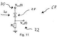
- Fig. 11 shows a circuit diagram of a photodetector 68 according to an embodiment of the present invention.
- the photodetector 68 comprises the RTD 28, a voltage source 70 for biasing the RTD 28 and comprises a detection apparatus 72.
- the photodetector 68 has a serial resistance R s as is indicated in Fig. 11 .
- the voltage source 70 can provide a constant voltage or a varying voltage for biasing the RTD 28. As a result a tunneling current can flow through the RTD 28, wherein the tunneling current is based on hole conduction.
- the tunneling current and/or the change thereof can be determined by measuring a voltage drop over the serial resistance R s . The measurement can be performed by the detection apparatus 72 which in the example of Fig. 11 may be a voltmeter.
- an ampere meter can be used as detection apparatus 72.
- the ampere meter can be used to directly determine the current through the RTD 28.
- the voltage source 70 can be replaced by a current source (not shown).
- the detection apparatus 62 can correspond to a voltmeter for measuring the voltage drop over the RTD 28.
- the detection apparatus 62 is arranged between the RTD 28 and the current source (not shown).
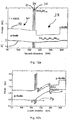
- Figs. 12a and 12b show energy diagrams of a layer structure according to a first embodiment of the present invention.
- the diagrams of Figs. 12a and 12b correspond to a temperature of 300 K.
- the layer structure of Figs. 12a and 12b comprises the following layers in the following order from left to right: a p-doped GaSb layer 40, a first barrier layer 32 of AlAsSb, an inter-barrier layer 34 of GaSb, a second barrier layer 36 of AlAsSb, an absorption layer 38 of GaInAsSb and a p-doped layer of GaSb. It is noted that the order does not correspond to the order of Fig. 10b .
- the absorption layer 38 of the example of Fig. 12 has a thickness of about 110 nm.
- no bias is applied to the layer structure and in Fig. 12b a bias is applied leading to a resonant tunneling current 74 based on hole conduction through the double barrier in the valence band 16.
- a bias is applied leading to a resonant tunneling current 74 based on hole conduction through the double barrier in the valence band 16.
- the photo excited electrons move towards the double barrier in the conduction band 14 because of the applied bias.
- the valence band 16 has only small offsets which are close to zero whereas the conduction band 14 has comparatively large offsets.
- One of the large offsets in the conduction band 14 forms an electron barrier in the conduction band 14 in addition to the double barrier in the conduction band 14. This additional electron barrier can help to prevent the photogenerated electrons from tunneling through the double barrier in the conduction band 14.
- the tunneling current 74 can be effectively created or developed in the valence band 16 while the electrons accumulate in the triangular well created at the additional electron barrier close to the double barrier structure in the conductance band 14 without tunneling through the double barrier, as indicated in Fig. 12b .
- the accumulated electrons cause a slight energetic distortion of the double barriers by a variation of the local electrostatic potential leading to a change of the current voltage characteristic and therefore to a change of the tunneling current 74. This allows for efficient detection of the photons which create photo excited electrons.
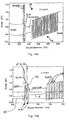
- Figs. 13a and 13b show a layer structure according to a second embodiment.
- the layer structure of Figs. 13a and 13b differs from the layer structure of Figs. 12a and 12b in that each of the AlAsSb barrier layers is replaced by a double layer having a layer of InAs and a layer of AlAsSb, as is illustrated in Figs. 13b .
- the resulting change in the conduction band 14 and in the valence band 16 with respect to the layer structure of Fig. 12 is indicated by dashed lines in Fig. 13a .
- the additional layers of InAs provide electron wells in the conduction band 14 and increase the barriers in the valence band 16.
- Fig. 13b shows the wave function 76 of an electron which is confined in a well provided by a layer of InAs. Because the InAs layer and therefore the well is part of the barrier structure, photogenerated electrons can be confined or localized in close proximity to the quantum well for holes which is provided by the barrier structure, such that the Coulomb interaction can be increased. Thereby also the change of the resonant tunneling current can be increased which can lead to a larger detection signal and to a higher amplification.
- the lifetime of accumulated electrons can be increased leading to a longer period in which the resonant tunneling current is changed. This can contribute to a further amplification of the detection signal, because the detection signal can be generated based on an integration over time of the resonant tunneling current or the change thereof.
- the electron wells can therefore strongly contribute to increase the sensitivity for photodetection even further.
- the InAs layers in the example of Fig. 13 not only provide wells in the conduction band 14 but simultaneously increase the barrier height in the valence band 16. This reduces the non-resonant tunneling of holes through the barrier structure, such that an undesired leaking current can be reduced more effectively. Further, the increased barrier height leads to sharper energy states for holes in the well which is provided between the barrier layers in the valence band 16. This leads to a current voltage characteristic with a more pronounced resonance and NDR region. This further increases the sensitivity or allows detecting with the same sensitivity at higher temperatures.
- Figs. 14a and 14b show an energy band diagram of a layer structure according to a third embodiment which is biased by a voltage of 0.8 V.
- the layer structure of the third embodiment differs from the first and second embodiments of Figs. 12 and 13 in that the absorption layer 38 further comprises a superlattice 78.
- the superlattice comprises a layer sequence of alternating layers of GaInSb and InAs.
- the superlattice 78 comprises 26 layers of GaInSb and 27 layers of InAs.
- the total thickness of this superlattice 78 in the illustrated example is about 130 nm.
- the absorption layer 38 comprises a layer of GaInAsSb having a thickness of about 35 nm.
- the superlattice 78 provides the advantage that the effective band gap for photon absorption can be specifically adjusted.
- the absorption wavelength can be specifically adjusted in a range between 3 ⁇ m and 30 ⁇ m.
- the adjustment of the effective absorption wavelength of a superlattice 78 can be performed by adjusting the thickness of the individual layers of the superlattice 78.
- the layer of GaInAsSb adjacent to the double barrier provides the advantage of having an electron well in front of the double barrier which allows effectively accumulating the electrons at the double barrier and preventing them from tunneling through the double barrier in the conduction band 14. This increases the detection signal and reduces the leaking current which leads to a higher sensitivity.
- the sequence "GaSb-barrier layer structure-GaInAsSb" allows for an efficient tunneling in the valence band 16, because directly behind the barrier layer structure there is no significant offset in the valence band 16 which could impede the hole conduction.
- the wave function 76 of a confined electron Fig. 14b shows a wave function 80 of a hole which is tunneling through the double barrier in the conduction band 16.
Landscapes
- Light Receiving Elements (AREA)
Claims (13)
- Photodétecteur (68) comprenant une structure de couche pour photodétection, dans lequel la structure de couche est formée intégralement et comprend- une structure à tunnel de résonance pour la tunnelisation de trou dans la bande de valence, dans lequel la structure à tunnel de résonance comprend• une structure de couche de barrière pour accumuler des électrons induits par photon dans la bande de conduction au niveau de la structure de couche de barrière ou dans la structure de couche de barrière, la structure de couche de barrière comprenant au moins deux couches de barrière (32, 36) séparées par au moins une couche inter-barrière (34), et• une première couche dopée p (40), et- une couche d'absorption (38), la couche d'absorption (38) comprenant GaInAsSb permettant l'absorption photoélectrique de photons dans une plage comprise entre 1,7 µm et 5 µm et/ou comprend un superréseau de GaInSb/InAs permettant l'absorption photoélectrique de photons dans une plage comprise entre 2,5 µm et 30 µm, la structure de couche formée intégralement comprend GaSb et/ou des semi-conducteurs à composé ternaire, quaternaire ou quinternaire avec un paramètre cristallin compris entre 6,05 Å et 6,15 Å et/ou est à base de GaSb.
- Photodétecteur (68) selon la revendication 1, dans lequel la structure à tunnel de résonance est unipolaire et comprend en outre une deuxième couche dopée p (52), dans lequel la structure de couche de barrière et la couche d'absorption (38) sont agencées entre la première couche dopée p (40) et la deuxième couche dopée p (52).
- Photodétecteur selon l'une des revendications précédentes, dans lequel la structure de couche intégralement formée est agencée sur un substrat (30) comprenant GaSb.
- Photodétecteur (68) selon l'une des revendications précédentes, dans lequel la couche de barrières (32, 36) comprend AlAsSb.
- Photodétecteur (68) selon l'une des revendications précédentes, dans lequel la structure de couche de barrière comprend une structure de double barrière AlAsSb/GaSb/AlAsSb.
- Photodétecteur (68) selon l'une des revendications précédentes, dans lequel la structure de couche comprend une couche qui fournit un puits à électrons dans la bande de conduction (14), dans lequel la couche est agencée au niveau de la structure de couche de barrière et est agencée entre la structure de couche de barrière et la couche d'absorption (38).
- Photodétecteur (68) selon l'une des revendications précédentes, dans lequel la structure de couche de barrière comprend deux doubles couches spatialement séparées (32, 36), dans lequel chaque double couche (32, 36) comprend- une première couche d'un premier matériau (AlAsSb) fournissant une barrière d'électrons dans la bande de conduction (14) et une première barrière de trou dans la bande de valence (16), et- une deuxième couche d'un deuxième matériau (InAs) fournissant un puits d'électron dans la bande de conduction (14) et une deuxième barrière de trou dans la bande de valence (16).
- Photodétecteur (68) selon la revendication 7, dans lequel la deuxième barrière de trou est plus haute que la première barrière de trou.
- Photodétecteur (68) selon l'une des revendications précédentes, dans lequel la structure de couche de barrière deux doubles couches spatialement séparées (32, 36), dans lequel chaque double couche (32, 36) comprend- une première couche comprenant AlAsSb et- une deuxième couche comprenant InAs.
- Photodétecteur (68) selon l'une des revendications précédentes, dans lequel au moins l'une des couches dopées p (40, 52) et la structure de couche de barrière sont comprises dans une structure de mesa (60), dans le photodétecteur (68) comprenant en outre une couche de scellement isolante (62) recouvrant la structure de mesa (60).
- Photodétecteur (68) selon la revendication 10, dans lequel la couche d'étanchéité (62) est formée de GaAs ou InAs.
- Photodétecteur (68) selon l'une des revendications précédentes, comprenant en outre- une source de tension ou de courant (70) pour polariser la structure à tunnel de résonance pour fournir un courant tunnel (74), le courant tunnel (74) étant basé sur la conduction de trou,- un appareil de détection (72) pour détecter un changement du courant tunnel (74), le changement étant induit par absorption de photons.
- Procédé de formation d'une structure de couche pour un photodétecteur (68), ledit procédé comprenant les étapes suivantes :- la fourniture d'un substrat (30),- la croissance d'une structure de couche (50) comprenant une structure à tunnel de résonance sur le substrat, ladite croissance comprenant les étapes suivantes :• la croissance d'une structure à tunnel de résonance pour la tunnelisation de trou dans la bande de valence, comprenant∘ la croissance d'une couche dopée p (40),∘ la croissance d'une structure de couche de barrière pour accumuler des électrons induits par photon dans la bande de conduction au niveau de la structure de couche de barrière ou dans la structure de couche de barrière, comprenanta la croissance d'une première couche de barrière (32),a la croissance d'une couche inter-barrière (34) sur la première couche de barrière (32),▪ la croissance d'une deuxième couche de barrière (36) sur la couche inter-barrière (34), et• la croissance d'une couche d'absorption (38), la couche d'absorption (38) comprenant GaInAsSb permettant l'absorption photoélectrique de photons dans une plage comprise entre 1,7 µm et 5 µm et/ou comprend un superréseau de GaInSb/InAs permettant l'absorption photoélectrique de photons dans une plage comprise entre 2,5 µm et 30 µm, dans lequel la structure de couche comprend GaSb et/ou des semi-conducteurs à composé ternaire, quaternaire ou quinternaire avec un paramètre cristallin compris entre 6,05 Å et 6,15 Å et/ou est à base de GaSb.
Priority Applications (1)
| Application Number | Priority Date | Filing Date | Title |
|---|---|---|---|
| EP15181128.8A EP3131124B1 (fr) | 2015-08-14 | 2015-08-14 | Photodétecteur infrarouge basé sur une diode à effet tunnel résonant |
Applications Claiming Priority (1)
| Application Number | Priority Date | Filing Date | Title |
|---|---|---|---|
| EP15181128.8A EP3131124B1 (fr) | 2015-08-14 | 2015-08-14 | Photodétecteur infrarouge basé sur une diode à effet tunnel résonant |
Publications (2)
| Publication Number | Publication Date |
|---|---|
| EP3131124A1 EP3131124A1 (fr) | 2017-02-15 |
| EP3131124B1 true EP3131124B1 (fr) | 2019-09-25 |
Family
ID=53836008
Family Applications (1)
| Application Number | Title | Priority Date | Filing Date |
|---|---|---|---|
| EP15181128.8A Active EP3131124B1 (fr) | 2015-08-14 | 2015-08-14 | Photodétecteur infrarouge basé sur une diode à effet tunnel résonant |
Country Status (1)
| Country | Link |
|---|---|
| EP (1) | EP3131124B1 (fr) |
Families Citing this family (1)
| Publication number | Priority date | Publication date | Assignee | Title |
|---|---|---|---|---|
| CN109524453B (zh) * | 2018-10-22 | 2022-03-29 | 杭州电子科技大学 | 一种GaN基高压整流共振隧穿二极管 |
Family Cites Families (5)
| Publication number | Priority date | Publication date | Assignee | Title |
|---|---|---|---|---|
| KR970011140B1 (ko) | 1993-12-08 | 1997-07-07 | 한국전자통신연구원 | 공명 투과광전 소자의 구조 |
| JPH08111540A (ja) | 1994-08-19 | 1996-04-30 | Texas Instr Inc <Ti> | 透明な共振トンネリング光検出器 |
| KR100244524B1 (ko) * | 1997-01-16 | 2000-02-01 | 정선종 | 광제어공명투과다이오드 |
| US8143648B1 (en) | 2006-08-11 | 2012-03-27 | Hrl Laboratories, Llc | Unipolar tunneling photodetector |
| WO2009106595A1 (fr) * | 2008-02-26 | 2009-09-03 | Julius-Maximilians-Universität Würzburg | Capteur de quantités électromagnétiques et procédé de mesure de quantités électromagnétiques |
-
2015
- 2015-08-14 EP EP15181128.8A patent/EP3131124B1/fr active Active
Non-Patent Citations (1)
| Title |
|---|
| None * |
Also Published As
| Publication number | Publication date |
|---|---|
| EP3131124A1 (fr) | 2017-02-15 |
Similar Documents
| Publication | Publication Date | Title |
|---|---|---|
| Jiang et al. | In 0.6 Ga 0.4 As/GaAs quantum-dot infrared photodetector with operating temperature up to 260 K | |
| US7737411B2 (en) | nBn and pBp infrared detectors with graded barrier layer, graded absorption layer, or chirped strained layer super lattice absorption layer | |
| US10062794B2 (en) | Resonant-cavity infrared photodetectors with fully-depleted absorbers | |
| US8928029B2 (en) | Single-band and dual-band infrared detectors | |
| CN107210326A (zh) | 电磁波检测器以及电磁波检测器阵列 | |
| US8076740B2 (en) | Photo detector with a quantum dot layer | |
| US9799785B1 (en) | Unipolar barrier dual-band infrared detectors | |
| Fuchs et al. | Optoelectronic properties of photodiodes for the mid-and far-infrared based on the InAs/GaSb/AlSb materials family | |
| US9748427B1 (en) | MWIR photodetector with compound barrier with P-N junction | |
| JP2016213362A (ja) | アバランシェフォトダイオード | |
| JP2001060699A (ja) | 光検出器 | |
| JPH07202247A (ja) | 共鳴トンネリング光電素子およびその製造方法 | |
| US8143648B1 (en) | Unipolar tunneling photodetector | |
| JP4829004B2 (ja) | 光検知装置およびその製造方法 | |
| EP3131124B1 (fr) | Photodétecteur infrarouge basé sur une diode à effet tunnel résonant | |
| Krapf et al. | Infrared multispectral detection using Si/Si x Ge 1− x quantum well infrared photodetectors | |
| US6747296B1 (en) | Avalanche photodiode multiplication region and avalanche photodiode with low impact ionization rate ratio | |
| Bansal et al. | Photodetectors for security application | |
| US9570646B2 (en) | Nano avalanche photodiode architecture for photon detection | |
| JP6563835B2 (ja) | 受光素子 | |
| Lin et al. | High-temperature operation GaSb/GaAs quantum-dot infrared photodetectors | |
| KR960004594B1 (ko) | 적외선 광 검출기 | |
| Zeiri et al. | Modeling of electrical and optical characteristics of near room-temperature CdS/ZnSe based NIR photodetectors | |
| US11264526B1 (en) | Infrared photodetector with optical amplification and low dark current | |
| Alomari et al. | Resonant Tunneling Diode Based Photodetectors Design Rules for Telecom Applications |
Legal Events
| Date | Code | Title | Description |
|---|---|---|---|
| PUAI | Public reference made under article 153(3) epc to a published international application that has entered the european phase |
Free format text: ORIGINAL CODE: 0009012 |
|
| STAA | Information on the status of an ep patent application or granted ep patent |
Free format text: STATUS: REQUEST FOR EXAMINATION WAS MADE |
|
| 17P | Request for examination filed |
Effective date: 20160803 |
|
| AK | Designated contracting states |
Kind code of ref document: A1 Designated state(s): AL AT BE BG CH CY CZ DE DK EE ES FI FR GB GR HR HU IE IS IT LI LT LU LV MC MK MT NL NO PL PT RO RS SE SI SK SM TR |
|
| AX | Request for extension of the european patent |
Extension state: BA ME |
|
| GRAP | Despatch of communication of intention to grant a patent |
Free format text: ORIGINAL CODE: EPIDOSNIGR1 |
|
| STAA | Information on the status of an ep patent application or granted ep patent |
Free format text: STATUS: GRANT OF PATENT IS INTENDED |
|
| INTG | Intention to grant announced |
Effective date: 20190403 |
|
| GRAS | Grant fee paid |
Free format text: ORIGINAL CODE: EPIDOSNIGR3 |
|
| GRAA | (expected) grant |
Free format text: ORIGINAL CODE: 0009210 |
|
| STAA | Information on the status of an ep patent application or granted ep patent |
Free format text: STATUS: THE PATENT HAS BEEN GRANTED |
|
| AK | Designated contracting states |
Kind code of ref document: B1 Designated state(s): AL AT BE BG CH CY CZ DE DK EE ES FI FR GB GR HR HU IE IS IT LI LT LU LV MC MK MT NL NO PL PT RO RS SE SI SK SM TR |
|
| REG | Reference to a national code |
Ref country code: GB Ref legal event code: FG4D |
|
| REG | Reference to a national code |
Ref country code: CH Ref legal event code: EP |
|
| REG | Reference to a national code |
Ref country code: AT Ref legal event code: REF Ref document number: 1184685 Country of ref document: AT Kind code of ref document: T Effective date: 20191015 |
|
| REG | Reference to a national code |
Ref country code: IE Ref legal event code: FG4D |
|
| REG | Reference to a national code |
Ref country code: DE Ref legal event code: R096 Ref document number: 602015038565 Country of ref document: DE |
|
| REG | Reference to a national code |
Ref country code: NL Ref legal event code: MP Effective date: 20190925 |
|
| PG25 | Lapsed in a contracting state [announced via postgrant information from national office to epo] |
Ref country code: LT Free format text: LAPSE BECAUSE OF FAILURE TO SUBMIT A TRANSLATION OF THE DESCRIPTION OR TO PAY THE FEE WITHIN THE PRESCRIBED TIME-LIMIT Effective date: 20190925 Ref country code: SE Free format text: LAPSE BECAUSE OF FAILURE TO SUBMIT A TRANSLATION OF THE DESCRIPTION OR TO PAY THE FEE WITHIN THE PRESCRIBED TIME-LIMIT Effective date: 20190925 Ref country code: BG Free format text: LAPSE BECAUSE OF FAILURE TO SUBMIT A TRANSLATION OF THE DESCRIPTION OR TO PAY THE FEE WITHIN THE PRESCRIBED TIME-LIMIT Effective date: 20191225 Ref country code: FI Free format text: LAPSE BECAUSE OF FAILURE TO SUBMIT A TRANSLATION OF THE DESCRIPTION OR TO PAY THE FEE WITHIN THE PRESCRIBED TIME-LIMIT Effective date: 20190925 Ref country code: NO Free format text: LAPSE BECAUSE OF FAILURE TO SUBMIT A TRANSLATION OF THE DESCRIPTION OR TO PAY THE FEE WITHIN THE PRESCRIBED TIME-LIMIT Effective date: 20191225 Ref country code: HR Free format text: LAPSE BECAUSE OF FAILURE TO SUBMIT A TRANSLATION OF THE DESCRIPTION OR TO PAY THE FEE WITHIN THE PRESCRIBED TIME-LIMIT Effective date: 20190925 |
|
| REG | Reference to a national code |
Ref country code: LT Ref legal event code: MG4D |
|
| PG25 | Lapsed in a contracting state [announced via postgrant information from national office to epo] |
Ref country code: RS Free format text: LAPSE BECAUSE OF FAILURE TO SUBMIT A TRANSLATION OF THE DESCRIPTION OR TO PAY THE FEE WITHIN THE PRESCRIBED TIME-LIMIT Effective date: 20190925 Ref country code: LV Free format text: LAPSE BECAUSE OF FAILURE TO SUBMIT A TRANSLATION OF THE DESCRIPTION OR TO PAY THE FEE WITHIN THE PRESCRIBED TIME-LIMIT Effective date: 20190925 Ref country code: GR Free format text: LAPSE BECAUSE OF FAILURE TO SUBMIT A TRANSLATION OF THE DESCRIPTION OR TO PAY THE FEE WITHIN THE PRESCRIBED TIME-LIMIT Effective date: 20191226 |
|
| REG | Reference to a national code |
Ref country code: AT Ref legal event code: MK05 Ref document number: 1184685 Country of ref document: AT Kind code of ref document: T Effective date: 20190925 |
|
| PG25 | Lapsed in a contracting state [announced via postgrant information from national office to epo] |
Ref country code: AT Free format text: LAPSE BECAUSE OF FAILURE TO SUBMIT A TRANSLATION OF THE DESCRIPTION OR TO PAY THE FEE WITHIN THE PRESCRIBED TIME-LIMIT Effective date: 20190925 Ref country code: PL Free format text: LAPSE BECAUSE OF FAILURE TO SUBMIT A TRANSLATION OF THE DESCRIPTION OR TO PAY THE FEE WITHIN THE PRESCRIBED TIME-LIMIT Effective date: 20190925 Ref country code: AL Free format text: LAPSE BECAUSE OF FAILURE TO SUBMIT A TRANSLATION OF THE DESCRIPTION OR TO PAY THE FEE WITHIN THE PRESCRIBED TIME-LIMIT Effective date: 20190925 Ref country code: IT Free format text: LAPSE BECAUSE OF FAILURE TO SUBMIT A TRANSLATION OF THE DESCRIPTION OR TO PAY THE FEE WITHIN THE PRESCRIBED TIME-LIMIT Effective date: 20190925 Ref country code: PT Free format text: LAPSE BECAUSE OF FAILURE TO SUBMIT A TRANSLATION OF THE DESCRIPTION OR TO PAY THE FEE WITHIN THE PRESCRIBED TIME-LIMIT Effective date: 20200127 Ref country code: EE Free format text: LAPSE BECAUSE OF FAILURE TO SUBMIT A TRANSLATION OF THE DESCRIPTION OR TO PAY THE FEE WITHIN THE PRESCRIBED TIME-LIMIT Effective date: 20190925 Ref country code: ES Free format text: LAPSE BECAUSE OF FAILURE TO SUBMIT A TRANSLATION OF THE DESCRIPTION OR TO PAY THE FEE WITHIN THE PRESCRIBED TIME-LIMIT Effective date: 20190925 Ref country code: NL Free format text: LAPSE BECAUSE OF FAILURE TO SUBMIT A TRANSLATION OF THE DESCRIPTION OR TO PAY THE FEE WITHIN THE PRESCRIBED TIME-LIMIT Effective date: 20190925 Ref country code: RO Free format text: LAPSE BECAUSE OF FAILURE TO SUBMIT A TRANSLATION OF THE DESCRIPTION OR TO PAY THE FEE WITHIN THE PRESCRIBED TIME-LIMIT Effective date: 20190925 |
|
| PG25 | Lapsed in a contracting state [announced via postgrant information from national office to epo] |
Ref country code: SM Free format text: LAPSE BECAUSE OF FAILURE TO SUBMIT A TRANSLATION OF THE DESCRIPTION OR TO PAY THE FEE WITHIN THE PRESCRIBED TIME-LIMIT Effective date: 20190925 Ref country code: CZ Free format text: LAPSE BECAUSE OF FAILURE TO SUBMIT A TRANSLATION OF THE DESCRIPTION OR TO PAY THE FEE WITHIN THE PRESCRIBED TIME-LIMIT Effective date: 20190925 Ref country code: IS Free format text: LAPSE BECAUSE OF FAILURE TO SUBMIT A TRANSLATION OF THE DESCRIPTION OR TO PAY THE FEE WITHIN THE PRESCRIBED TIME-LIMIT Effective date: 20200224 Ref country code: SK Free format text: LAPSE BECAUSE OF FAILURE TO SUBMIT A TRANSLATION OF THE DESCRIPTION OR TO PAY THE FEE WITHIN THE PRESCRIBED TIME-LIMIT Effective date: 20190925 |
|
| REG | Reference to a national code |
Ref country code: DE Ref legal event code: R097 Ref document number: 602015038565 Country of ref document: DE |
|
| PG2D | Information on lapse in contracting state deleted |
Ref country code: IS |
|
| PG25 | Lapsed in a contracting state [announced via postgrant information from national office to epo] |
Ref country code: DK Free format text: LAPSE BECAUSE OF FAILURE TO SUBMIT A TRANSLATION OF THE DESCRIPTION OR TO PAY THE FEE WITHIN THE PRESCRIBED TIME-LIMIT Effective date: 20190925 Ref country code: IS Free format text: LAPSE BECAUSE OF FAILURE TO SUBMIT A TRANSLATION OF THE DESCRIPTION OR TO PAY THE FEE WITHIN THE PRESCRIBED TIME-LIMIT Effective date: 20200126 |
|
| PLBE | No opposition filed within time limit |
Free format text: ORIGINAL CODE: 0009261 |
|
| STAA | Information on the status of an ep patent application or granted ep patent |
Free format text: STATUS: NO OPPOSITION FILED WITHIN TIME LIMIT |
|
| 26N | No opposition filed |
Effective date: 20200626 |
|
| PG25 | Lapsed in a contracting state [announced via postgrant information from national office to epo] |
Ref country code: SI Free format text: LAPSE BECAUSE OF FAILURE TO SUBMIT A TRANSLATION OF THE DESCRIPTION OR TO PAY THE FEE WITHIN THE PRESCRIBED TIME-LIMIT Effective date: 20190925 |
|
| PG25 | Lapsed in a contracting state [announced via postgrant information from national office to epo] |
Ref country code: MC Free format text: LAPSE BECAUSE OF FAILURE TO SUBMIT A TRANSLATION OF THE DESCRIPTION OR TO PAY THE FEE WITHIN THE PRESCRIBED TIME-LIMIT Effective date: 20190925 |
|
| REG | Reference to a national code |
Ref country code: CH Ref legal event code: PL |
|
| PG25 | Lapsed in a contracting state [announced via postgrant information from national office to epo] |
Ref country code: LU Free format text: LAPSE BECAUSE OF NON-PAYMENT OF DUE FEES Effective date: 20200814 Ref country code: LI Free format text: LAPSE BECAUSE OF NON-PAYMENT OF DUE FEES Effective date: 20200831 Ref country code: CH Free format text: LAPSE BECAUSE OF NON-PAYMENT OF DUE FEES Effective date: 20200831 |
|
| REG | Reference to a national code |
Ref country code: BE Ref legal event code: MM Effective date: 20200831 |
|
| PG25 | Lapsed in a contracting state [announced via postgrant information from national office to epo] |
Ref country code: BE Free format text: LAPSE BECAUSE OF NON-PAYMENT OF DUE FEES Effective date: 20200831 Ref country code: IE Free format text: LAPSE BECAUSE OF NON-PAYMENT OF DUE FEES Effective date: 20200814 |
|
| PG25 | Lapsed in a contracting state [announced via postgrant information from national office to epo] |
Ref country code: TR Free format text: LAPSE BECAUSE OF FAILURE TO SUBMIT A TRANSLATION OF THE DESCRIPTION OR TO PAY THE FEE WITHIN THE PRESCRIBED TIME-LIMIT Effective date: 20190925 Ref country code: MT Free format text: LAPSE BECAUSE OF FAILURE TO SUBMIT A TRANSLATION OF THE DESCRIPTION OR TO PAY THE FEE WITHIN THE PRESCRIBED TIME-LIMIT Effective date: 20190925 Ref country code: CY Free format text: LAPSE BECAUSE OF FAILURE TO SUBMIT A TRANSLATION OF THE DESCRIPTION OR TO PAY THE FEE WITHIN THE PRESCRIBED TIME-LIMIT Effective date: 20190925 |
|
| PG25 | Lapsed in a contracting state [announced via postgrant information from national office to epo] |
Ref country code: MK Free format text: LAPSE BECAUSE OF FAILURE TO SUBMIT A TRANSLATION OF THE DESCRIPTION OR TO PAY THE FEE WITHIN THE PRESCRIBED TIME-LIMIT Effective date: 20190925 |
|
| PGFP | Annual fee paid to national office [announced via postgrant information from national office to epo] |
Ref country code: GB Payment date: 20220630 Year of fee payment: 8 |
|
| PGFP | Annual fee paid to national office [announced via postgrant information from national office to epo] |
Ref country code: DE Payment date: 20220705 Year of fee payment: 8 |
|
| PGFP | Annual fee paid to national office [announced via postgrant information from national office to epo] |
Ref country code: FR Payment date: 20220709 Year of fee payment: 8 |
|
| REG | Reference to a national code |
Ref country code: DE Ref legal event code: R119 Ref document number: 602015038565 Country of ref document: DE |
|
| GBPC | Gb: european patent ceased through non-payment of renewal fee |
Effective date: 20230814 |
|
| PG25 | Lapsed in a contracting state [announced via postgrant information from national office to epo] |
Ref country code: GB Free format text: LAPSE BECAUSE OF NON-PAYMENT OF DUE FEES Effective date: 20230814 |
|
| PG25 | Lapsed in a contracting state [announced via postgrant information from national office to epo] |
Ref country code: GB Free format text: LAPSE BECAUSE OF NON-PAYMENT OF DUE FEES Effective date: 20230814 Ref country code: FR Free format text: LAPSE BECAUSE OF NON-PAYMENT OF DUE FEES Effective date: 20230831 Ref country code: DE Free format text: LAPSE BECAUSE OF NON-PAYMENT OF DUE FEES Effective date: 20240301 |