EP3131209B1 - Nfc-antennenarchitektur für eine mobilkommunikationsvorrichtung mit einem einteiligen metallgehäuse - Google Patents
Nfc-antennenarchitektur für eine mobilkommunikationsvorrichtung mit einem einteiligen metallgehäuse Download PDFInfo
- Publication number
- EP3131209B1 EP3131209B1 EP16183202.7A EP16183202A EP3131209B1 EP 3131209 B1 EP3131209 B1 EP 3131209B1 EP 16183202 A EP16183202 A EP 16183202A EP 3131209 B1 EP3131209 B1 EP 3131209B1
- Authority
- EP
- European Patent Office
- Prior art keywords
- nfc
- drive
- antenna
- antennas
- communication device
- Prior art date
- Legal status (The legal status is an assumption and is not a legal conclusion. Google has not performed a legal analysis and makes no representation as to the accuracy of the status listed.)
- Active
Links
Images




Classifications
-
- H—ELECTRICITY
- H04—ELECTRIC COMMUNICATION TECHNIQUE
- H04W—WIRELESS COMMUNICATION NETWORKS
- H04W4/00—Services specially adapted for wireless communication networks; Facilities therefor
- H04W4/80—Services using short range communication, e.g. near-field communication [NFC], radio-frequency identification [RFID] or low energy communication
-
- H—ELECTRICITY
- H01—ELECTRIC ELEMENTS
- H01Q—ANTENNAS, i.e. RADIO AERIALS
- H01Q1/00—Details of, or arrangements associated with, antennas
- H01Q1/12—Supports; Mounting means
- H01Q1/22—Supports; Mounting means by structural association with other equipment or articles
- H01Q1/24—Supports; Mounting means by structural association with other equipment or articles with receiving set
- H01Q1/241—Supports; Mounting means by structural association with other equipment or articles with receiving set used in mobile communications, e.g. GSM
- H01Q1/242—Supports; Mounting means by structural association with other equipment or articles with receiving set used in mobile communications, e.g. GSM specially adapted for hand-held use
- H01Q1/243—Supports; Mounting means by structural association with other equipment or articles with receiving set used in mobile communications, e.g. GSM specially adapted for hand-held use with built-in antennas
-
- H—ELECTRICITY
- H01—ELECTRIC ELEMENTS
- H01Q—ANTENNAS, i.e. RADIO AERIALS
- H01Q21/00—Antenna arrays or systems
- H01Q21/30—Combinations of separate antenna units operating in different wavebands and connected to a common feeder system
-
- H—ELECTRICITY
- H01—ELECTRIC ELEMENTS
- H01Q—ANTENNAS, i.e. RADIO AERIALS
- H01Q5/00—Arrangements for simultaneous operation of antennas on two or more different wavebands, e.g. dual-band or multi-band arrangements
- H01Q5/30—Arrangements for providing operation on different wavebands
- H01Q5/307—Individual or coupled radiating elements, each element being fed in an unspecified way
- H01Q5/342—Individual or coupled radiating elements, each element being fed in an unspecified way for different propagation modes
- H01Q5/35—Individual or coupled radiating elements, each element being fed in an unspecified way for different propagation modes using two or more simultaneously fed points
-
- H—ELECTRICITY
- H01—ELECTRIC ELEMENTS
- H01Q—ANTENNAS, i.e. RADIO AERIALS
- H01Q7/00—Loop antennas with a substantially uniform current distribution around the loop and having a directional radiation pattern in a plane perpendicular to the plane of the loop
-
- H—ELECTRICITY
- H01—ELECTRIC ELEMENTS
- H01Q—ANTENNAS, i.e. RADIO AERIALS
- H01Q7/00—Loop antennas with a substantially uniform current distribution around the loop and having a directional radiation pattern in a plane perpendicular to the plane of the loop
- H01Q7/04—Screened antennas
-
- H—ELECTRICITY
- H04—ELECTRIC COMMUNICATION TECHNIQUE
- H04B—TRANSMISSION
- H04B5/00—Near-field transmission systems, e.g. inductive or capacitive transmission systems
- H04B5/20—Near-field transmission systems, e.g. inductive or capacitive transmission systems characterised by the transmission technique; characterised by the transmission medium
- H04B5/24—Inductive coupling
- H04B5/26—Inductive coupling using coils
-
- H—ELECTRICITY
- H04—ELECTRIC COMMUNICATION TECHNIQUE
- H04B—TRANSMISSION
- H04B5/00—Near-field transmission systems, e.g. inductive or capacitive transmission systems
- H04B5/40—Near-field transmission systems, e.g. inductive or capacitive transmission systems characterised by components specially adapted for near-field transmission
- H04B5/43—Antennas
-
- H—ELECTRICITY
- H01—ELECTRIC ELEMENTS
- H01Q—ANTENNAS, i.e. RADIO AERIALS
- H01Q21/00—Antenna arrays or systems
- H01Q21/28—Combinations of substantially independent non-interacting antenna units or systems
-
- H—ELECTRICITY
- H01—ELECTRIC ELEMENTS
- H01Q—ANTENNAS, i.e. RADIO AERIALS
- H01Q9/00—Electrically-short antennas having dimensions not more than twice the operating wavelength and consisting of conductive active radiating elements
- H01Q9/04—Resonant antennas
- H01Q9/30—Resonant antennas with feed to end of elongated active element, e.g. unipole
- H01Q9/42—Resonant antennas with feed to end of elongated active element, e.g. unipole with folded element, the folded parts being spaced apart a small fraction of the operating wavelength
-
- H—ELECTRICITY
- H04—ELECTRIC COMMUNICATION TECHNIQUE
- H04B—TRANSMISSION
- H04B1/00—Details of transmission systems, not covered by a single one of groups H04B3/00 - H04B13/00; Details of transmission systems not characterised by the medium used for transmission
- H04B1/38—Transceivers, i.e. devices in which transmitter and receiver form a structural unit and in which at least one part is used for functions of transmitting and receiving
- H04B1/3827—Portable transceivers
-
- H—ELECTRICITY
- H04—ELECTRIC COMMUNICATION TECHNIQUE
- H04M—TELEPHONIC COMMUNICATION
- H04M2250/00—Details of telephonic subscriber devices
- H04M2250/04—Details of telephonic subscriber devices including near field communication means, e.g. RFID
Definitions
- the present disclosure is related generally to wireless communication technologies for mobile devices, and, more particularly, to a system and method for near field communications (NFC) to and from a device having a metal housing.
- NFC near field communications
- NFC antenna is typically a conductive loop that is configured to transmit and detect magnetic fields.
- An NFC antenna is commonly referred to as an NFC coil.
- An NFC coil is often placed behind the back housing of a mobile communication device.
- Portable communication devices such as cellular phones have typically incorporated a non-conductive back housing (e.g. plastic), or an appropriate opening in a conductive back housing, to allow an embedded NFC coil to freely communicate.
- the opening is necessary otherwise the magnetic fields generated by the NFC coil would be trapped between the conductive internal components of the mobile device and the conductive housing.
- the opening in the conductive back housing provides a mechanism to interrupt eddy currents induced by the NFC coil and allows for NFC communication.
- internal NFC coils typically require an open (nonconductive) path through the back of the device.
- cellular phone manufacturers are increasingly employing exterior housings fabricated from metal alloys.
- mobile communication devices are handled frequently, and plastic housings are weaker than metal ones of similar thickness, hence allowing more frequent damage and breakage.
- a metal housing with an opening over an internal NFC coil is still weaker than a unibody metal construction, is more expensive and complex to manufacture than a unibody construction, and is aesthetically less pleasing than a unibody construction.
- US 2015/044963 describes a device in which WLAN and near field communications (NFC) use the same coil antenna.
- portable communication devices generally incorporate a plastic housing, or an opening in a conductive housing, to allow the embedded NFC coil of the device to freely communicate.
- the latter prevents the generation of opposing magnetic fields induced by eddy currents, which occurs if the NFC coil is completely covered by a conductive material.
- both of these options provide a housing that is weaker and more expensive than one constructed from a metal unibody.
- a mobile communication device having a single-piece metal housing with openings at both ends.
- the openings on the housing form a plurality of arms that function as antennas in the finished device.
- the housing may be configured with two arms at one end of the housing (e.g. the top side) and two arms at the opposite end of the housing (e.g., the bottom side).
- Various ones of these antennas may be used for GPS geo-location services, WiFi communications, cellular communications or a combination of these.
- two of the antennas are selectively chosen in an embodiment to create a loop antenna usable for NFC signal transmission and reception. This use does not prevent or interfere with the continued use of each antenna for GPS geo-location services, WiFi communications, cellular communications, or a combination of these.
- Figure 1 illustrates an example mobile device within which embodiments of the disclosed principles may be implemented, it will be appreciated that other device types may be used, including but not limited to laptop computers, tablet computers, embedded automobile computing systems and so on.
- the schematic diagram of Figure 1 shows an exemplary device 110 forming part of an environment within which aspects of the present disclosure may be implemented.
- the schematic diagram illustrates a user device 110 including several exemplary components. It will be appreciated that additional or alternative components may be used in a given implementation depending upon user preference, component availability, price point and other considerations.
- the components of the user device 110 include a display screen 120, applications (e.g., programs) 130, a processor 140, a memory 150, one or more input components 160 such as speech and text input facilities, and one or more output components 170 such as text and audible output facilities, e.g., one or more speakers.
- the processor 140 can be any of a microprocessor, microcomputer, application-specific integrated circuit, or the like.
- the processor 140 can be implemented by one or more microprocessors or controllers from any desired family or manufacturer.
- the memory 150 may reside on the same integrated circuit as the processor 140. Additionally or alternatively, the memory 150 may be accessed via a network, e.g., via cloud-based storage.
- the memory 150 may include a random access memory (i.e., Synchronous Dynamic Random Access Memory (SDRAM), Dynamic Random Access Memory (DRAM), RAMBUS Dynamic Random Access Memory (RDRM) or any other type of random access memory device or system). Additionally or alternatively, the memory 150 may include a read only memory (i.e., a hard drive, flash memory or any other desired type of memory device).
- the information that is stored by the memory 150 can include program code associated with one or more operating systems or applications as well as informational data, e.g., program parameters, process data, etc.
- the operating system and applications are typically implemented via executable instructions stored in a non-transitory computer readable medium (e.g., memory 150) to control basic functions of the electronic device 110.
- Such functions may include, for example, interaction among various internal components and storage and retrieval of applications and data to and from the memory 150.
- applications typically utilize the operating system to provide more specific functionality, such as file system service and handling of protected and unprotected data stored in the memory 150.
- applications may provide standard or required functionality of the user device 110, in other cases applications provide optional or specialized functionality, and may be supplied by third party vendors or the device manufacturer.
- informational data e.g., program parameters and process data
- this non-executable information can be referenced, manipulated, or written by the operating system or an application.
- informational data can include, for example, data that are preprogrammed into the device during manufacture, data that are created by the device or added by the user, or any of a variety of types of information that are uploaded to, downloaded from, or otherwise accessed at servers or other devices with which the device is in communication during its ongoing operation.
- the device 110 includes software and hardware networking components 180 to allow communications to and from the device.
- networking components provide wireless networking functionality, although wired networking may additionally or alternatively be supported.
- the networking components 180 include an NFC antenna.
- a power supply 190 such as a battery or fuel cell, may be included for providing power to the device 110 and its components. All or some of the internal components communicate with one another by way of one or more shared or dedicated internal communication links 195, such as an internal bus.
- the device 110 is programmed such that the processor 140 and memory 150 interact with the other components of the device 110 to perform a variety of functions.
- the processor 140 may include or implement various modules and execute programs for initiating different activities such as launching an application, transferring data and toggling through various graphical user interface objects (e.g., toggling through various display icons that are linked to executable applications).
- FIG. 2 this figure shows a metal unibody housing 201 for a portable communication device such as device 110 of Figure 1 .
- the illustrated housing is simply an example, and that other configurations of unibody housing may be used. That said, in the illustrated example, the metal housing 201 is formed having a first opening 203 and a second opening 205, with the first opening 203 being located in the upper portion of the metal housing 201 and the second opening 205 being located in the lower portion of the metal housing 201.
- a first break 207 is located in the top of the metal housing 201, causing the first opening 203 to be non-closed.
- a second break 209 located in the bottom of the metal housing 201 causes the second opening 205 to be non-closed.
- a pair of antenna arms 211, 213 is formed at the top of the metal housing 201 and another pair of antenna arms 215, 217 is formed at the bottom of the metal housing 201.
- the remainder of the metal housing 201 may be referred to herein for clarity when required as the main body 219 of the metal housing 201.
- the antennas 211, 213, 215 and 217 may be referred to herein as antenna 1 (ant-1), antenna 2 (ant-2), antenna 3 (ant-3) and antenna 4 (ant-4).
- top antennas such as the ant-1 and ant-2 antennas (211, 213) in the illustrated example, may be used for GPS geo-location services, WiFi communications, and cellular communications, while the bottom antennas such as the ant-3 and ant-4 antennas (215, 217) may be dedicated to support cellular communications. It will be appreciated by those of skill in the art that other antenna assignments may be used instead.
- two of the available antennas are reused to provide NFC communications.
- the two top antennas ant-1 (211) and ant-2 (213) may be differentially driven to form a single turn loop antenna surrounding the top opening 203.
- the effective circuit configuration of this architecture including GPS, WiFi and cellular communications, is shown schematically in Figure 3 .
- the device may include a WiFi transceiver 301 and a GPS receiver 309 linked to ant-1 (211) via a diplexer.
- the device may also include a cellular transceiver 303 which may be linked to ant-2 (213), which operates at a different frequency than that used by the WiFi transceiver 301 and GPS receiver 309.
- a WiFi transceiver 301, a GPS receiver 309 and a cellular transceiver 303 may be linked to ant-1 (211) via a triplexer.
- the device may also include a secondary WiFi transceiver and it may share ant-2 (213) with the cellular transceiver via high band antenna switching modules 311.
- the device need not implement GPS, WiFi and cellular communications via the top antennas 211, 213; rather, the example of Figure 3 is given to illustrate the fact that, in an embodiment of the disclosed principles, the use of either or both of the top antennas for GPS, WiFi or cellular communications does not interfere with their use for NFC communications. Similarly, the use of both of the top antennas for NFC communications does not interfere with their use for GPS, WiFi or cellular communications.
- the frequency at which NFC signals are generated is set by relevant standards at 13.56 MHz.
- the frequency band at which GPS signals are received by mobile devices is centered at 1.575 GHz.
- WiFi transceivers communicate on frequency bands that are centered at 2.45 GHz and 5.2 GHz and cellular transceivers communicate between the frequencies of 500 MHz and 3 GHz.
- a differential drive circuit 305 for NFC communications is shown.
- the differential drive circuit 305 is linked to the NFC controller 307, which handles the encoding and decoding of NFC signals and executes the instructions provided by the applications processor 140 of Figure 1 .
- the differential drive circuit 305 is also linked to both ant-1 (211) and ant-2 (213), with each antenna forming a respective side of the differential, and in essence, creating a single turn loop antenna for NFC communications.
- the differential drive circuit 305 contains components to decouple the NFC transceiver from the GPS receiver, WiFi transceivers and cellular transceiver.
- the spectral separation between the operating frequency of the NFC transceiver and the others allows for a simple decoupling mechanism consisting of an inductor and a capacitor.
- a set of inductors placed between the NFC antenna impedance match and the physical connections to ant-1 (211) and ant-2 (213) may decouple the NFC transceiver from the other transceivers using these top antennas.
- a series capacitor between the other transceivers and their respective top antenna (ant-1, ant-2 or both depending on the embodiment) may decouple these transceivers from the NFC transceiver.
- the decoupling can also be achieved in numerous other ways, such as switching.
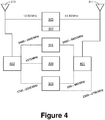
- Figure 4 shows a modular schematic for implementing the architectures shown in Figure 3 . Although those of skill in the art will appreciate that other circuit constructions may be used to implement the disclosed principles, Figure 4 provides an example to clarify operation of the system for those of skill in the art as well as those of more casual acquaintance with the art.
- the WiFi transceiver 301, the GPS receiver 309, and the cellular transceiver 303 are linked to a dedicated antenna via a multiplexer 403.
- Multiplexer 403 may route the incoming GPS signals in 1575 MHz band to the GPS receiver, WiFi signals in 2400-2495 MHz band to the WiFi transceiver, and cellular signals in 1700-2200 MHz band to the cellular transceiver.
- the dedicated antenna may be, for example, ant-2 (213).
- the other antenna 211 is linked to the WiFi transceiver 301 and also to the cellular receiver 303 through a high band antenna switch module 401 or the like.
- incoming low-band cellular signals such as those in 698-960 MHz band and high-band cellular signals such as those in the 2300-2400 MHz band and the 2500-2690 MHz band are switched to the cellular transceiver 303.
- incoming 2400 MHz (2.4 GHz) WiFi signals are switched to the WiFi transceiver 301.
- the switch module operates to allow both outgoing 2.4 GHz WiFi signals and outgoing high band cellular signals to share a single antenna 213.
- the cellular transceiver 303 and WiFi transceiver 301 may also be multiplexed to and from the shared antenna 213.
- cellular transceiver 303, WiFi transceiver 301, and GPS receiver 309 may be multiplexed to and from the shared antenna 211.
- the cellular transceiver 303 will have priority with respect to usage of a shared antenna in a switched module based embodiment.
- the differential drive circuit 305 for NFC communications is shown linked between ant-1 (211) and ant-2 (213).
- the differential drive circuit 305 is part of, or is controlled by, an NFC controller 307. Given the frequency difference between NFC communications and WiFi or cellular communications and the existence of LC based decoupling circuitry, the use of ant-1 (211) and ant-2 (213) to provide NFC communications does not affect the use of these antennas for WiFi, GPS or cellular signal reception and transmission.
- FIG. 5A , 5B and 5C illustrate more precisely the manner in which the antennas 211, 213 are driven for NFC communications.
- ant-1 (211) is excited via coupling from a nearby trace 509 which is linked to the antenna drive 503.
- antenna drive 503 is directly connected to the ant-1 (such as 502 of Figure 5B and 504 of Figure 5C )
- a decoupling capacitor 513 is connected in series with the antenna drive 503. The purpose of the series capacitor is to block the energy generated by the NFC antenna drive 501 from coupling into the antenna drive 503.
- the drive 503 may be connected directly to the WiFi transceiver 301, GPS receiver 309 and cellular transceiver 303 ( Figure 4 ).
- the antenna drive 503 is referenced to ground, as provided by the main body 219 of the metal housing 201.
- the other antenna, ant-2 (213) is excited directly by an antenna drive 505.
- a decoupling capacitor 513 is connected in series with the antenna drive 505 to block the NFC energy from the antenna drive 501.
- antenna drive 505 may be connected to a cellular transceiver 303 ( Figure 4 ) and also to a WiFi transceiver through a switch 401.
- the antenna drive 505 is also referenced to ground, as provided by the main body 219 of the metal housing 201. Note that in another embodiment (not shown), ant-2 may be excited by a nearby trace that is connected to the antenna drive 505. In this case, a series decoupling may not be necessary since the antenna drive 505 would be physically disconnected from ant-2.
- NFC loop 507 is created by both antennas 211, 213 and the main body 219 of the metal housing 201 and it is differentially driven at the gap between the antennas 211, 213.
- the NFC antenna drive 501 is exciting ant-1 (211) with one pole of the differential feed and is exciting ant-2 (213) with the other pole of the differential feed.
- the NFC antenna drive 501 and decoupling inductors 511 are part of the differential drive circuit 305, which is subsequently connected to the NFC controller 307 ( Figure 3 ). In the embodiments shown in Figures 5A , 5B and 5C , decoupling inductors 511 are employed to block the electromagnetic energy produced by antenna drives 503 and 505 from coupling into the NFC antenna drive 501.
- the NFC antenna drive 501 is connected to ant-1 via a mechanical connection 515 and to ant-2 via a mechanical connection 517.
- the antenna drive 503 is connected to ant-1 via a mechanical connection 521 and the antenna drive 505 is connected to ant-2 via a mechanical connection 519.
- the mechanical connections 515 and 521 are combined into 523, while keeping the decoupling inductors and capacitors in place.
- mechanical connections 517 and 519 are combined into 525.
- the device 110 is enabled to operate as an NFC card emulator, an NFC card reader or an NFC peer.
- the device 110 responds to NFC polling pulses from an external source by emitting an NFC response mimicking a particular NFC card.
- the device 110 polls an NFC card (actual or emulated) and receives and processes an appropriate NFC response.
- the device communicates with another NFC enabled device via the transmission and reception of NFC transmissions.
- the physical layout of the NFC coil 507 employs a smaller physical loop along the larger path that is shown in dashed outline in Figure 5 .
- the smaller loop 603 and its relationship to the larger loop 601 are shown in Figure 6 .
- This smaller loop 603 not only increases the inherent inductance of the NFC coil, but also its placement between ant-1 (211) and ant-2 (213) reduces the likelihood of a null in the near magnetic field.
- the larger loop 601 corresponding to the dashed path 507 of Figures 5A , 5B and 5C , connects in series to a smaller loop 603 having the same orientation.
- the multi-turn smaller loop 603 increases the inductance of the NFC coil substantially over that of the single-turn larger loop 601 alone.
- the smaller loop 603 is positioned in the central upper section of the device where it overlies an audio speaker 605 of the device.
- the audio speaker 605 is shown by a circular dashed outline.
- a ferrite shield 607 can be located beneath the smaller loop 603. This placement allows interference reduction between the internal metallic components of the device and the NFC operation.
- the metal provides shielding between the GPS, WiFi or cellular antennas in the vicinity and the lossy ferrite material in 607, thereby mitigating the potential performance deficiencies.
- the loop structure shown in Figure 6 is also employed in an embodiment to provide wireless charging for the device.
- the A4WP protocol operates at 6.78 MHz, which corresponds to one half of the typical NFC frequency.
- the A4WP protocol uses resonant coupling rather than inductive coupling, such that a low inductance device coil may be coupled if the real impedance of the device coil is matched to the real impedance of the driving coil.
- the driving coil may be located within a table, desk or shelf whereupon a device may be placed for wireless charging.
- the device charging coil is as shown in Figure 6 but is located at the opposite end of the device from the NFC coil. Moreover, a capacitance may be provided in series or parallel with the coil to match the real impedance of the device charging coil to that of the charging coil. In this way, a portable communications device having a unibody metal back housing may nonetheless support wireless charging as well as WiFi, cellular, and NFC capabilities.
Landscapes
- Engineering & Computer Science (AREA)
- Computer Networks & Wireless Communication (AREA)
- Signal Processing (AREA)
- Near-Field Transmission Systems (AREA)
- Telephone Function (AREA)
Claims (13)
- Mobile elektronische Kommunikationsvorrichtung, Folgendes umfassend:eine leitende Schleife mit einer ersten Unterbrechung (207), die zwei mit dem Rest der Schleife verbundene Antennen (211, 213) bildet;einen mit einer ersten der Antennen verbundenen Mobilfunk-Antennentreiber (503, 505);einen mit einer zweiten der Antennen verbundenen WLAN-Antennentreiber (505, 503); undeinen zwischen der ersten und der zweiten Antenne angeschlossenen Differential-Nahfeldkommunikationstreiber (NFC-Treiber) (501), so dass die leitende Schleife eine NFC-Antenne bildet.
- Mobile elektronische Kommunikationsvorrichtung nach Anspruch 1, wobei der WLAN-Antennentreiber umschaltbar mit der ersten Antenne verbunden ist.
- Mobile elektronische Kommunikationsvorrichtung nach Anspruch 1 oder 2, wobei der Mobilfunk-Antennentreiber und der WLAN-Antennentreiber mit einer auf Masse bezogenen Common-Mode-Zuleitung verbunden sind.
- Mobile elektronische Kommunikationsvorrichtung nach einem vorhergehenden Anspruch, wobei der Differential-NFC-Treiber physikalisch mit dem Mobilfunk-Treiber und dem WLAN-Treiber verbunden ist, aber elektrisch mit einer Schaltung aus einer Spule und einem Kondensator (LC-Schaltung) von diesen getrennt ist.
- Mobile elektronische Kommunikationsvorrichtung nach einem vorhergehenden Anspruch, ferner umfassend eine sekundäre NFC-Schleife mit mehreren Windungen, die mit der NFC-Schleife verbunden ist und durch den NFC-Treiber in der gleichen Orientierung wie die NFC-Schleife aktiviert wird.
- Mobile elektronische Kommunikationsvorrichtung nach einem vorhergehenden Anspruch, wobei bei jeder der ersten und der zweiten Antenne ein Ende mit Masse verbunden ist und ein anderes Ende auf Schwebepotential liegt, wobei:der Mobilfunk-Antennentreiber zwischen dem auf Schwebepotential liegenden Ende der ersten Antenne und Masse angeschlossen ist;der WLAN-Antennentreiber zwischen dem auf Schwebepotential liegenden Ende der zweiten Antenne und Masse angeschlossen ist; undder Differential-NFC-Treiber zwischen den auf Schwebepotential liegenden Enden der ersten und der zweiten Antenne angeschlossen ist.
- Mobile elektronische Kommunikationsvorrichtung nach einem vorhergehenden Anspruch, Folgendes umfassend:ein als einteiliges Metallgehäuse ausgebildetes Gehäuse, wobei das einteilige Metallgehäuse eine erste Öffnung an einem ersten Ende aufweist, wobei die erste Unterbrechung sich in dem distalen Rand der ersten Öffnung befindet, so dass der unterbrochene distale Rand der ersten Öffnung die beiden Antennen bildet, wobei:die beiden Antennen mit einem Rest des einteiligen Metallgehäuses verbunden sind; undder Differential-NFC-Treiber zwischen der ersten und der zweiten Antenne angeschlossen ist, um die NFC-Schleife zu aktivieren, die die erste und die zweite Antenne und den Rest des einteiligen Metallgehäuses umfasst.
- Mobile elektronische Kommunikationsvorrichtung nach Anspruch 7, wobei eine der ersten und der zweiten Antenne GPS-Positionierungsdienste, WLAN-Kommunikationen, Mobilfunkkommunikationen oder eine Kombination von diesen unterstützt.
- Mobile elektronische Kommunikationsvorrichtung nach Anspruch 7 oder 8, wobei der Differential-NFC-Treiber und ein Nicht-NFC-Antennentreiber gemeinsam eine mechanische Verbindung mit der ersten Antenne nutzen, und der Differential-NFC-Treiber und der Nicht-NFC-Antennentreiber gemeinsam eine mechanische Verbindung mit der zweiten Antenne nutzen.
- Mobile elektronische Kommunikationsvorrichtung nach einem der Ansprüche 7 bis 9, wobei die eine der ersten und der zweiten Antenne zwischen WLAN-Kommunikationen und Mobilfunk-Kommunikationen umgeschaltet wird.
- Mobile elektronische Kommunikationsvorrichtung nach einem der Ansprüche 8 bis 10, wobei die eine der ersten und der zweiten Antenne WLAN-Kommunikationen, GPS-Positionierungsdienste und Mobilfunk-Kommunikationen multiplext.
- Mobile elektronische Kommunikationsvorrichtung nach einem der Ansprüche 7 bis 11, wobei der Differential-NFC-Treiber von dem Mobilfunk-Treiber und dem WLAN-Treiber mit einer Schaltung aus einer Spule und einem Kondensator (LC-Schaltung) entkoppelt ist.
- Mobile elektronische Kommunikationsvorrichtung nach einem der Ansprüche 7 bis 12, wobei der Rest des einteiligen Metallgehäuses eine Referenzmasse darstellt.
Applications Claiming Priority (1)
| Application Number | Priority Date | Filing Date | Title |
|---|---|---|---|
| US14/824,240 US9801006B2 (en) | 2015-08-12 | 2015-08-12 | NFC antenna architecture for mobile communication device with single-piece metal housing |
Publications (2)
| Publication Number | Publication Date |
|---|---|
| EP3131209A1 EP3131209A1 (de) | 2017-02-15 |
| EP3131209B1 true EP3131209B1 (de) | 2019-02-27 |
Family
ID=56681980
Family Applications (1)
| Application Number | Title | Priority Date | Filing Date |
|---|---|---|---|
| EP16183202.7A Active EP3131209B1 (de) | 2015-08-12 | 2016-08-08 | Nfc-antennenarchitektur für eine mobilkommunikationsvorrichtung mit einem einteiligen metallgehäuse |
Country Status (2)
| Country | Link |
|---|---|
| US (1) | US9801006B2 (de) |
| EP (1) | EP3131209B1 (de) |
Families Citing this family (23)
| Publication number | Priority date | Publication date | Assignee | Title |
|---|---|---|---|---|
| US9882415B2 (en) * | 2015-10-01 | 2018-01-30 | Motorola Mobility Llc | Wireless charging architecture for mobile communication device with single piece metal housing |
| US10079922B2 (en) | 2016-03-11 | 2018-09-18 | Microsoft Technology Licensing, Llc | Conductive structural members acting as NFC antenna |
| US9766666B1 (en) * | 2016-07-13 | 2017-09-19 | Google Inc. | Metallic housing for short-range wireless communication |
| US10283843B2 (en) * | 2016-08-12 | 2019-05-07 | Motorola Mobility Llc | Antenna system including closely spaced antennas adapted for operating at the same or similar frequencies |
| CN107123861A (zh) * | 2017-03-27 | 2017-09-01 | 联想(北京)有限公司 | 一种在终端上实现nfc天线的天线结构 |
| CN107613425A (zh) * | 2017-11-14 | 2018-01-19 | 金妙英 | 一种多功能便携式音响 |
| CN111052500B (zh) * | 2017-12-06 | 2021-02-23 | 华为技术有限公司 | 天线组件及移动终端 |
| US11502388B2 (en) * | 2018-01-22 | 2022-11-15 | Stmicroelectronics, Inc. | Electronic device including an antenna |
| US10396438B1 (en) | 2018-05-31 | 2019-08-27 | Motorola Mobility Llc | Antenna system and electronic device including one or more conductive elements for use with a differential and an alternative signal source |
| EP3918663B1 (de) * | 2019-02-25 | 2023-06-21 | Huawei Technologies Co., Ltd. | Antennenstruktur mit zwei anschlüssen |
| EP3916907B1 (de) * | 2019-02-27 | 2025-05-21 | Huawei Technologies Co., Ltd. | Antennenvorrichtung und elektronische vorrichtung |
| CN112448146B (zh) * | 2019-08-30 | 2022-03-01 | Oppo广东移动通信有限公司 | 天线装置、电子设备及天线切换方法 |
| CN114760870A (zh) * | 2019-11-28 | 2022-07-15 | 日本烟草国际股份有限公司 | 具有近场通信的电子烟 |
| CN112993540B (zh) * | 2019-12-13 | 2023-07-28 | Oppo广东移动通信有限公司 | 电子设备 |
| FR3105697B1 (fr) * | 2019-12-19 | 2022-04-29 | Proton World Int Nv | Configuration d'un terminal mobile NFC |
| FR3105506B1 (fr) | 2019-12-19 | 2023-05-19 | St Microelectronics Rousset | Configuration d'un terminal mobile NFC |
| WO2021136052A1 (zh) * | 2019-12-31 | 2021-07-08 | Oppo广东移动通信有限公司 | 天线装置及电子设备 |
| CN113131196B (zh) * | 2019-12-31 | 2025-02-14 | Oppo广东移动通信有限公司 | 天线装置及电子设备 |
| EP4111536B1 (de) * | 2020-04-06 | 2025-12-31 | Huawei Technologies Co., Ltd. | Antennenanordnung mit zwei betriebsarten |
| US11605896B2 (en) | 2020-04-16 | 2023-03-14 | Motorola Mobility Llc | Communication device having metallic frame that includes a T-shaped slot antenna |
| CN116231304A (zh) * | 2020-06-05 | 2023-06-06 | 华为技术有限公司 | 一种电子设备 |
| US20240258716A1 (en) * | 2023-01-27 | 2024-08-01 | Canon Kabushiki Kaisha | Wireless communication apparatus, electronic equipment, and radiographing system |
| CN118508049A (zh) * | 2023-02-16 | 2024-08-16 | 荣耀终端有限公司 | 一种天线系统及电子设备 |
Family Cites Families (12)
| Publication number | Priority date | Publication date | Assignee | Title |
|---|---|---|---|---|
| US8344959B2 (en) * | 2009-04-30 | 2013-01-01 | Nokia Corporation | Multiprotocol antenna for wireless systems |
| US20100279734A1 (en) * | 2009-04-30 | 2010-11-04 | Nokia Corporation | Multiprotocol Antenna For Wireless Systems |
| US8779999B2 (en) * | 2011-09-30 | 2014-07-15 | Google Inc. | Antennas for computers with conductive chassis |
| US9148190B1 (en) * | 2012-01-17 | 2015-09-29 | Amazon Technologies, Inc. | Multipurpose coils |
| US9125007B2 (en) | 2012-03-30 | 2015-09-01 | Intel Corporation | Near field communications (NFC) coil with embedded wireless antenna |
| US9112280B2 (en) * | 2012-07-10 | 2015-08-18 | Sony Corporation | Antenna apparatus and terminal device associated with antenna apparatus |
| US9793616B2 (en) | 2012-11-19 | 2017-10-17 | Apple Inc. | Shared antenna structures for near-field communications and non-near-field communications circuitry |
| US9807815B2 (en) * | 2012-12-11 | 2017-10-31 | Intel Corporation | Apparatus, system and method of simultaneous connectivity to location origin transceivers |
| US9160068B2 (en) * | 2013-05-09 | 2015-10-13 | Google Technology Holdings LLC | Systems and methods for antenna arrangements in an electronic device |
| US10312593B2 (en) | 2014-04-16 | 2019-06-04 | Apple Inc. | Antennas for near-field and non-near-field communications |
| US9666934B2 (en) * | 2015-04-08 | 2017-05-30 | Motorola Mobility Llc | Antenna link in ultra-thin device with single-piece metal housing |
| US9882415B2 (en) * | 2015-10-01 | 2018-01-30 | Motorola Mobility Llc | Wireless charging architecture for mobile communication device with single piece metal housing |
-
2015
- 2015-08-12 US US14/824,240 patent/US9801006B2/en active Active
-
2016
- 2016-08-08 EP EP16183202.7A patent/EP3131209B1/de active Active
Non-Patent Citations (1)
| Title |
|---|
| None * |
Also Published As
| Publication number | Publication date |
|---|---|
| EP3131209A1 (de) | 2017-02-15 |
| US9801006B2 (en) | 2017-10-24 |
| US20170048649A1 (en) | 2017-02-16 |
Similar Documents
| Publication | Publication Date | Title |
|---|---|---|
| EP3131209B1 (de) | Nfc-antennenarchitektur für eine mobilkommunikationsvorrichtung mit einem einteiligen metallgehäuse | |
| US9882415B2 (en) | Wireless charging architecture for mobile communication device with single piece metal housing | |
| JP6100903B2 (ja) | 電気エネルギーハーベスティングおよび/または無線通信のための装置および方法 | |
| US10256526B2 (en) | Near field communication antenna, near field communication device and mobile device having the same | |
| US10325708B2 (en) | Spiral near field communication (NFC) antenna coil | |
| KR102283428B1 (ko) | 휴대 기기의 하우징, 근거리 무선 통신 송수신기 및 휴대 기기 | |
| US8907859B2 (en) | Edge-emitting antennas for ultra slim wireless mobile devices | |
| CN110350311B (zh) | 移动设备中的nfc天线 | |
| US20140125548A1 (en) | Apparatus With A Near Field Coupling Member And Method For Communication | |
| CN104466363A (zh) | 用于可穿戴式装置的nfc天线结构及智能手表 | |
| US9281562B2 (en) | Apparatus with antenna and method for wireless communication | |
| US10950941B2 (en) | Conductive structural member acting as single-ended NFC antenna | |
| CN105490004A (zh) | 一种移动终端天线系统及移动终端 | |
| JP2016519525A (ja) | 無線通信装置及び方法 | |
| CN106663874A (zh) | 用于无线通信的装置和方法 | |
| EP3041085B1 (de) | Kommunikationsendgerät | |
| US10903562B2 (en) | Batteries as antenna for device | |
| US9098789B2 (en) | RFID communication circuit for an electronic device and corresponding methods | |
| EP2639881B1 (de) | Kommunikationsvorrichtung und drehbares Antennenelement darin | |
| CN107331951A (zh) | Nfc和无线充电二合一的天线及其控制方法 | |
| US9648150B1 (en) | One piece conductive housing with incorporated antenna for use in an electronic device | |
| US20130147679A1 (en) | Antenna structure of handheld device | |
| US9722312B2 (en) | Loop antenna with a magnetically coupled element | |
| US20250357962A1 (en) | Electronic device comprising antenna | |
| KR20260050904A (ko) | 안테나를 포함하는 전자 장치 |
Legal Events
| Date | Code | Title | Description |
|---|---|---|---|
| PUAI | Public reference made under article 153(3) epc to a published international application that has entered the european phase |
Free format text: ORIGINAL CODE: 0009012 |
|
| STAA | Information on the status of an ep patent application or granted ep patent |
Free format text: STATUS: THE APPLICATION HAS BEEN PUBLISHED |
|
| AK | Designated contracting states |
Kind code of ref document: A1 Designated state(s): AL AT BE BG CH CY CZ DE DK EE ES FI FR GB GR HR HU IE IS IT LI LT LU LV MC MK MT NL NO PL PT RO RS SE SI SK SM TR |
|
| AX | Request for extension of the european patent |
Extension state: BA ME |
|
| STAA | Information on the status of an ep patent application or granted ep patent |
Free format text: STATUS: REQUEST FOR EXAMINATION WAS MADE |
|
| 17P | Request for examination filed |
Effective date: 20170816 |
|
| RBV | Designated contracting states (corrected) |
Designated state(s): AL AT BE BG CH CY CZ DE DK EE ES FI FR GB GR HR HU IE IS IT LI LT LU LV MC MK MT NL NO PL PT RO RS SE SI SK SM TR |
|
| GRAP | Despatch of communication of intention to grant a patent |
Free format text: ORIGINAL CODE: EPIDOSNIGR1 |
|
| STAA | Information on the status of an ep patent application or granted ep patent |
Free format text: STATUS: GRANT OF PATENT IS INTENDED |
|
| RIC1 | Information provided on ipc code assigned before grant |
Ipc: H01Q 1/24 20060101ALI20181008BHEP Ipc: H04B 5/00 20060101AFI20181008BHEP Ipc: H01Q 21/30 20060101ALI20181008BHEP Ipc: H01Q 9/42 20060101ALN20181008BHEP Ipc: H01Q 5/35 20150101ALN20181008BHEP Ipc: H01Q 7/00 20060101ALI20181008BHEP Ipc: H04B 1/3827 20150101ALN20181008BHEP |
|
| INTG | Intention to grant announced |
Effective date: 20181026 |
|
| GRAS | Grant fee paid |
Free format text: ORIGINAL CODE: EPIDOSNIGR3 |
|
| GRAA | (expected) grant |
Free format text: ORIGINAL CODE: 0009210 |
|
| STAA | Information on the status of an ep patent application or granted ep patent |
Free format text: STATUS: THE PATENT HAS BEEN GRANTED |
|
| AK | Designated contracting states |
Kind code of ref document: B1 Designated state(s): AL AT BE BG CH CY CZ DE DK EE ES FI FR GB GR HR HU IE IS IT LI LT LU LV MC MK MT NL NO PL PT RO RS SE SI SK SM TR |
|
| REG | Reference to a national code |
Ref country code: GB Ref legal event code: FG4D |
|
| REG | Reference to a national code |
Ref country code: CH Ref legal event code: EP |
|
| REG | Reference to a national code |
Ref country code: AT Ref legal event code: REF Ref document number: 1102836 Country of ref document: AT Kind code of ref document: T Effective date: 20190315 |
|
| REG | Reference to a national code |
Ref country code: IE Ref legal event code: FG4D |
|
| REG | Reference to a national code |
Ref country code: DE Ref legal event code: R096 Ref document number: 602016010281 Country of ref document: DE |
|
| REG | Reference to a national code |
Ref country code: NL Ref legal event code: FP |
|
| REG | Reference to a national code |
Ref country code: LT Ref legal event code: MG4D |
|
| PG25 | Lapsed in a contracting state [announced via postgrant information from national office to epo] |
Ref country code: LT Free format text: LAPSE BECAUSE OF FAILURE TO SUBMIT A TRANSLATION OF THE DESCRIPTION OR TO PAY THE FEE WITHIN THE PRESCRIBED TIME-LIMIT Effective date: 20190227 Ref country code: SE Free format text: LAPSE BECAUSE OF FAILURE TO SUBMIT A TRANSLATION OF THE DESCRIPTION OR TO PAY THE FEE WITHIN THE PRESCRIBED TIME-LIMIT Effective date: 20190227 Ref country code: FI Free format text: LAPSE BECAUSE OF FAILURE TO SUBMIT A TRANSLATION OF THE DESCRIPTION OR TO PAY THE FEE WITHIN THE PRESCRIBED TIME-LIMIT Effective date: 20190227 Ref country code: NO Free format text: LAPSE BECAUSE OF FAILURE TO SUBMIT A TRANSLATION OF THE DESCRIPTION OR TO PAY THE FEE WITHIN THE PRESCRIBED TIME-LIMIT Effective date: 20190527 Ref country code: PT Free format text: LAPSE BECAUSE OF FAILURE TO SUBMIT A TRANSLATION OF THE DESCRIPTION OR TO PAY THE FEE WITHIN THE PRESCRIBED TIME-LIMIT Effective date: 20190627 |
|
| PG25 | Lapsed in a contracting state [announced via postgrant information from national office to epo] |
Ref country code: IS Free format text: LAPSE BECAUSE OF FAILURE TO SUBMIT A TRANSLATION OF THE DESCRIPTION OR TO PAY THE FEE WITHIN THE PRESCRIBED TIME-LIMIT Effective date: 20190627 Ref country code: LV Free format text: LAPSE BECAUSE OF FAILURE TO SUBMIT A TRANSLATION OF THE DESCRIPTION OR TO PAY THE FEE WITHIN THE PRESCRIBED TIME-LIMIT Effective date: 20190227 Ref country code: GR Free format text: LAPSE BECAUSE OF FAILURE TO SUBMIT A TRANSLATION OF THE DESCRIPTION OR TO PAY THE FEE WITHIN THE PRESCRIBED TIME-LIMIT Effective date: 20190528 Ref country code: HR Free format text: LAPSE BECAUSE OF FAILURE TO SUBMIT A TRANSLATION OF THE DESCRIPTION OR TO PAY THE FEE WITHIN THE PRESCRIBED TIME-LIMIT Effective date: 20190227 Ref country code: RS Free format text: LAPSE BECAUSE OF FAILURE TO SUBMIT A TRANSLATION OF THE DESCRIPTION OR TO PAY THE FEE WITHIN THE PRESCRIBED TIME-LIMIT Effective date: 20190227 Ref country code: BG Free format text: LAPSE BECAUSE OF FAILURE TO SUBMIT A TRANSLATION OF THE DESCRIPTION OR TO PAY THE FEE WITHIN THE PRESCRIBED TIME-LIMIT Effective date: 20190527 |
|
| REG | Reference to a national code |
Ref country code: AT Ref legal event code: MK05 Ref document number: 1102836 Country of ref document: AT Kind code of ref document: T Effective date: 20190227 |
|
| PG25 | Lapsed in a contracting state [announced via postgrant information from national office to epo] |
Ref country code: AL Free format text: LAPSE BECAUSE OF FAILURE TO SUBMIT A TRANSLATION OF THE DESCRIPTION OR TO PAY THE FEE WITHIN THE PRESCRIBED TIME-LIMIT Effective date: 20190227 Ref country code: ES Free format text: LAPSE BECAUSE OF FAILURE TO SUBMIT A TRANSLATION OF THE DESCRIPTION OR TO PAY THE FEE WITHIN THE PRESCRIBED TIME-LIMIT Effective date: 20190227 Ref country code: RO Free format text: LAPSE BECAUSE OF FAILURE TO SUBMIT A TRANSLATION OF THE DESCRIPTION OR TO PAY THE FEE WITHIN THE PRESCRIBED TIME-LIMIT Effective date: 20190227 Ref country code: CZ Free format text: LAPSE BECAUSE OF FAILURE TO SUBMIT A TRANSLATION OF THE DESCRIPTION OR TO PAY THE FEE WITHIN THE PRESCRIBED TIME-LIMIT Effective date: 20190227 Ref country code: IT Free format text: LAPSE BECAUSE OF FAILURE TO SUBMIT A TRANSLATION OF THE DESCRIPTION OR TO PAY THE FEE WITHIN THE PRESCRIBED TIME-LIMIT Effective date: 20190227 Ref country code: EE Free format text: LAPSE BECAUSE OF FAILURE TO SUBMIT A TRANSLATION OF THE DESCRIPTION OR TO PAY THE FEE WITHIN THE PRESCRIBED TIME-LIMIT Effective date: 20190227 Ref country code: DK Free format text: LAPSE BECAUSE OF FAILURE TO SUBMIT A TRANSLATION OF THE DESCRIPTION OR TO PAY THE FEE WITHIN THE PRESCRIBED TIME-LIMIT Effective date: 20190227 Ref country code: SK Free format text: LAPSE BECAUSE OF FAILURE TO SUBMIT A TRANSLATION OF THE DESCRIPTION OR TO PAY THE FEE WITHIN THE PRESCRIBED TIME-LIMIT Effective date: 20190227 |
|
| REG | Reference to a national code |
Ref country code: DE Ref legal event code: R097 Ref document number: 602016010281 Country of ref document: DE |
|
| PG25 | Lapsed in a contracting state [announced via postgrant information from national office to epo] |
Ref country code: PL Free format text: LAPSE BECAUSE OF FAILURE TO SUBMIT A TRANSLATION OF THE DESCRIPTION OR TO PAY THE FEE WITHIN THE PRESCRIBED TIME-LIMIT Effective date: 20190227 Ref country code: SM Free format text: LAPSE BECAUSE OF FAILURE TO SUBMIT A TRANSLATION OF THE DESCRIPTION OR TO PAY THE FEE WITHIN THE PRESCRIBED TIME-LIMIT Effective date: 20190227 |
|
| PG25 | Lapsed in a contracting state [announced via postgrant information from national office to epo] |
Ref country code: AT Free format text: LAPSE BECAUSE OF FAILURE TO SUBMIT A TRANSLATION OF THE DESCRIPTION OR TO PAY THE FEE WITHIN THE PRESCRIBED TIME-LIMIT Effective date: 20190227 |
|
| PLBE | No opposition filed within time limit |
Free format text: ORIGINAL CODE: 0009261 |
|
| STAA | Information on the status of an ep patent application or granted ep patent |
Free format text: STATUS: NO OPPOSITION FILED WITHIN TIME LIMIT |
|
| 26N | No opposition filed |
Effective date: 20191128 |
|
| PG25 | Lapsed in a contracting state [announced via postgrant information from national office to epo] |
Ref country code: SI Free format text: LAPSE BECAUSE OF FAILURE TO SUBMIT A TRANSLATION OF THE DESCRIPTION OR TO PAY THE FEE WITHIN THE PRESCRIBED TIME-LIMIT Effective date: 20190227 |
|
| PG25 | Lapsed in a contracting state [announced via postgrant information from national office to epo] |
Ref country code: TR Free format text: LAPSE BECAUSE OF FAILURE TO SUBMIT A TRANSLATION OF THE DESCRIPTION OR TO PAY THE FEE WITHIN THE PRESCRIBED TIME-LIMIT Effective date: 20190227 |
|
| REG | Reference to a national code |
Ref country code: NL Ref legal event code: MM Effective date: 20190901 |
|
| PG25 | Lapsed in a contracting state [announced via postgrant information from national office to epo] |
Ref country code: LI Free format text: LAPSE BECAUSE OF NON-PAYMENT OF DUE FEES Effective date: 20190831 Ref country code: MC Free format text: LAPSE BECAUSE OF FAILURE TO SUBMIT A TRANSLATION OF THE DESCRIPTION OR TO PAY THE FEE WITHIN THE PRESCRIBED TIME-LIMIT Effective date: 20190227 Ref country code: CH Free format text: LAPSE BECAUSE OF NON-PAYMENT OF DUE FEES Effective date: 20190831 Ref country code: LU Free format text: LAPSE BECAUSE OF NON-PAYMENT OF DUE FEES Effective date: 20190808 |
|
| REG | Reference to a national code |
Ref country code: BE Ref legal event code: MM Effective date: 20190831 |
|
| PG25 | Lapsed in a contracting state [announced via postgrant information from national office to epo] |
Ref country code: NL Free format text: LAPSE BECAUSE OF NON-PAYMENT OF DUE FEES Effective date: 20190901 Ref country code: IE Free format text: LAPSE BECAUSE OF NON-PAYMENT OF DUE FEES Effective date: 20190808 Ref country code: FR Free format text: LAPSE BECAUSE OF NON-PAYMENT OF DUE FEES Effective date: 20190831 |
|
| PG25 | Lapsed in a contracting state [announced via postgrant information from national office to epo] |
Ref country code: BE Free format text: LAPSE BECAUSE OF NON-PAYMENT OF DUE FEES Effective date: 20190831 |
|
| PG25 | Lapsed in a contracting state [announced via postgrant information from national office to epo] |
Ref country code: CY Free format text: LAPSE BECAUSE OF FAILURE TO SUBMIT A TRANSLATION OF THE DESCRIPTION OR TO PAY THE FEE WITHIN THE PRESCRIBED TIME-LIMIT Effective date: 20190227 |
|
| PG25 | Lapsed in a contracting state [announced via postgrant information from national office to epo] |
Ref country code: MT Free format text: LAPSE BECAUSE OF FAILURE TO SUBMIT A TRANSLATION OF THE DESCRIPTION OR TO PAY THE FEE WITHIN THE PRESCRIBED TIME-LIMIT Effective date: 20190227 Ref country code: HU Free format text: LAPSE BECAUSE OF FAILURE TO SUBMIT A TRANSLATION OF THE DESCRIPTION OR TO PAY THE FEE WITHIN THE PRESCRIBED TIME-LIMIT; INVALID AB INITIO Effective date: 20160808 |
|
| PG25 | Lapsed in a contracting state [announced via postgrant information from national office to epo] |
Ref country code: MK Free format text: LAPSE BECAUSE OF FAILURE TO SUBMIT A TRANSLATION OF THE DESCRIPTION OR TO PAY THE FEE WITHIN THE PRESCRIBED TIME-LIMIT Effective date: 20190227 |
|
| P01 | Opt-out of the competence of the unified patent court (upc) registered |
Effective date: 20230627 |
|
| PGFP | Annual fee paid to national office [announced via postgrant information from national office to epo] |
Ref country code: DE Payment date: 20250827 Year of fee payment: 10 |
|
| PGFP | Annual fee paid to national office [announced via postgrant information from national office to epo] |
Ref country code: GB Payment date: 20250826 Year of fee payment: 10 |