EP3133375A1 - Capteur et générateur d'énergie à base d'induction électrostatique, procédé de détection et procédé de génération d'énergie - Google Patents
Capteur et générateur d'énergie à base d'induction électrostatique, procédé de détection et procédé de génération d'énergie Download PDFInfo
- Publication number
- EP3133375A1 EP3133375A1 EP15779244.1A EP15779244A EP3133375A1 EP 3133375 A1 EP3133375 A1 EP 3133375A1 EP 15779244 A EP15779244 A EP 15779244A EP 3133375 A1 EP3133375 A1 EP 3133375A1
- Authority
- EP
- European Patent Office
- Prior art keywords
- electrode layer
- component
- layer
- detected
- contact
- Prior art date
- Legal status (The legal status is an assumption and is not a legal conclusion. Google has not performed a legal analysis and makes no representation as to the accuracy of the status listed.)
- Granted
Links
Images


Classifications
-
- G—PHYSICS
- G01—MEASURING; TESTING
- G01D—MEASURING NOT SPECIALLY ADAPTED FOR A SPECIFIC VARIABLE; ARRANGEMENTS FOR MEASURING TWO OR MORE VARIABLES NOT COVERED IN A SINGLE OTHER SUBCLASS; TARIFF METERING APPARATUS; MEASURING OR TESTING NOT OTHERWISE PROVIDED FOR
- G01D5/00—Mechanical means for transferring the output of a sensing member; Means for converting the output of a sensing member to another variable where the form or nature of the sensing member does not constrain the means for converting; Transducers not specially adapted for a specific variable
- G01D5/12—Mechanical means for transferring the output of a sensing member; Means for converting the output of a sensing member to another variable where the form or nature of the sensing member does not constrain the means for converting; Transducers not specially adapted for a specific variable using electric or magnetic means
- G01D5/14—Mechanical means for transferring the output of a sensing member; Means for converting the output of a sensing member to another variable where the form or nature of the sensing member does not constrain the means for converting; Transducers not specially adapted for a specific variable using electric or magnetic means influencing the magnitude of a current or voltage
- G01D5/24—Mechanical means for transferring the output of a sensing member; Means for converting the output of a sensing member to another variable where the form or nature of the sensing member does not constrain the means for converting; Transducers not specially adapted for a specific variable using electric or magnetic means influencing the magnitude of a current or voltage by varying capacitance
-
- G—PHYSICS
- G01—MEASURING; TESTING
- G01D—MEASURING NOT SPECIALLY ADAPTED FOR A SPECIFIC VARIABLE; ARRANGEMENTS FOR MEASURING TWO OR MORE VARIABLES NOT COVERED IN A SINGLE OTHER SUBCLASS; TARIFF METERING APPARATUS; MEASURING OR TESTING NOT OTHERWISE PROVIDED FOR
- G01D5/00—Mechanical means for transferring the output of a sensing member; Means for converting the output of a sensing member to another variable where the form or nature of the sensing member does not constrain the means for converting; Transducers not specially adapted for a specific variable
- G01D5/12—Mechanical means for transferring the output of a sensing member; Means for converting the output of a sensing member to another variable where the form or nature of the sensing member does not constrain the means for converting; Transducers not specially adapted for a specific variable using electric or magnetic means
- G01D5/14—Mechanical means for transferring the output of a sensing member; Means for converting the output of a sensing member to another variable where the form or nature of the sensing member does not constrain the means for converting; Transducers not specially adapted for a specific variable using electric or magnetic means influencing the magnitude of a current or voltage
-
- H—ELECTRICITY
- H01—ELECTRIC ELEMENTS
- H01B—CABLES; CONDUCTORS; INSULATORS; SELECTION OF MATERIALS FOR THEIR CONDUCTIVE, INSULATING OR DIELECTRIC PROPERTIES
- H01B1/00—Conductors or conductive bodies characterised by the conductive materials; Selection of materials as conductors
- H01B1/02—Conductors or conductive bodies characterised by the conductive materials; Selection of materials as conductors mainly consisting of metals or alloys
-
- H—ELECTRICITY
- H01—ELECTRIC ELEMENTS
- H01B—CABLES; CONDUCTORS; INSULATORS; SELECTION OF MATERIALS FOR THEIR CONDUCTIVE, INSULATING OR DIELECTRIC PROPERTIES
- H01B3/00—Insulators or insulating bodies characterised by the insulating materials; Selection of materials for their insulating or dielectric properties
- H01B3/02—Insulators or insulating bodies characterised by the insulating materials; Selection of materials for their insulating or dielectric properties mainly consisting of inorganic substances
- H01B3/025—Other inorganic material
-
- H—ELECTRICITY
- H01—ELECTRIC ELEMENTS
- H01B—CABLES; CONDUCTORS; INSULATORS; SELECTION OF MATERIALS FOR THEIR CONDUCTIVE, INSULATING OR DIELECTRIC PROPERTIES
- H01B3/00—Insulators or insulating bodies characterised by the insulating materials; Selection of materials for their insulating or dielectric properties
- H01B3/02—Insulators or insulating bodies characterised by the insulating materials; Selection of materials for their insulating or dielectric properties mainly consisting of inorganic substances
- H01B3/10—Insulators or insulating bodies characterised by the insulating materials; Selection of materials for their insulating or dielectric properties mainly consisting of inorganic substances metallic oxides
-
- H—ELECTRICITY
- H01—ELECTRIC ELEMENTS
- H01B—CABLES; CONDUCTORS; INSULATORS; SELECTION OF MATERIALS FOR THEIR CONDUCTIVE, INSULATING OR DIELECTRIC PROPERTIES
- H01B3/00—Insulators or insulating bodies characterised by the insulating materials; Selection of materials for their insulating or dielectric properties
- H01B3/18—Insulators or insulating bodies characterised by the insulating materials; Selection of materials for their insulating or dielectric properties mainly consisting of organic substances
- H01B3/30—Insulators or insulating bodies characterised by the insulating materials; Selection of materials for their insulating or dielectric properties mainly consisting of organic substances plastics; resins; waxes
- H01B3/303—Macromolecular compounds obtained by reactions forming a linkage containing nitrogen with or without oxygen or carbon in the main chain of the macromolecule, not provided for in groups H01B3/38 or H01B3/302
- H01B3/305—Polyamides or polyesteramides
-
- H—ELECTRICITY
- H01—ELECTRIC ELEMENTS
- H01B—CABLES; CONDUCTORS; INSULATORS; SELECTION OF MATERIALS FOR THEIR CONDUCTIVE, INSULATING OR DIELECTRIC PROPERTIES
- H01B3/00—Insulators or insulating bodies characterised by the insulating materials; Selection of materials for their insulating or dielectric properties
- H01B3/18—Insulators or insulating bodies characterised by the insulating materials; Selection of materials for their insulating or dielectric properties mainly consisting of organic substances
- H01B3/30—Insulators or insulating bodies characterised by the insulating materials; Selection of materials for their insulating or dielectric properties mainly consisting of organic substances plastics; resins; waxes
- H01B3/303—Macromolecular compounds obtained by reactions forming a linkage containing nitrogen with or without oxygen or carbon in the main chain of the macromolecule, not provided for in groups H01B3/38 or H01B3/302
- H01B3/306—Polyimides or polyesterimides
-
- H—ELECTRICITY
- H01—ELECTRIC ELEMENTS
- H01B—CABLES; CONDUCTORS; INSULATORS; SELECTION OF MATERIALS FOR THEIR CONDUCTIVE, INSULATING OR DIELECTRIC PROPERTIES
- H01B3/00—Insulators or insulating bodies characterised by the insulating materials; Selection of materials for their insulating or dielectric properties
- H01B3/18—Insulators or insulating bodies characterised by the insulating materials; Selection of materials for their insulating or dielectric properties mainly consisting of organic substances
- H01B3/30—Insulators or insulating bodies characterised by the insulating materials; Selection of materials for their insulating or dielectric properties mainly consisting of organic substances plastics; resins; waxes
- H01B3/307—Other macromolecular compounds
-
- H—ELECTRICITY
- H01—ELECTRIC ELEMENTS
- H01B—CABLES; CONDUCTORS; INSULATORS; SELECTION OF MATERIALS FOR THEIR CONDUCTIVE, INSULATING OR DIELECTRIC PROPERTIES
- H01B3/00—Insulators or insulating bodies characterised by the insulating materials; Selection of materials for their insulating or dielectric properties
- H01B3/18—Insulators or insulating bodies characterised by the insulating materials; Selection of materials for their insulating or dielectric properties mainly consisting of organic substances
- H01B3/30—Insulators or insulating bodies characterised by the insulating materials; Selection of materials for their insulating or dielectric properties mainly consisting of organic substances plastics; resins; waxes
- H01B3/44—Insulators or insulating bodies characterised by the insulating materials; Selection of materials for their insulating or dielectric properties mainly consisting of organic substances plastics; resins; waxes vinyl resins; acrylic resins
- H01B3/447—Insulators or insulating bodies characterised by the insulating materials; Selection of materials for their insulating or dielectric properties mainly consisting of organic substances plastics; resins; waxes vinyl resins; acrylic resins from acrylic compounds
-
- H—ELECTRICITY
- H02—GENERATION; CONVERSION OR DISTRIBUTION OF ELECTRIC POWER
- H02N—ELECTRIC MACHINES NOT OTHERWISE PROVIDED FOR
- H02N1/00—Electrostatic generators or motors using a solid moving electrostatic charge carrier
- H02N1/04—Friction generators
-
- H—ELECTRICITY
- H02—GENERATION; CONVERSION OR DISTRIBUTION OF ELECTRIC POWER
- H02N—ELECTRIC MACHINES NOT OTHERWISE PROVIDED FOR
- H02N1/00—Electrostatic generators or motors using a solid moving electrostatic charge carrier
- H02N1/06—Influence generators
- H02N1/08—Influence generators with conductive charge carrier, i.e. capacitor machines
Definitions
- the present disclosure relates to a sensor, and in particular to a sensor and a sensing method for detecting movement of an object by means of electrostatic induction.
- the present disclosure also relates to a corresponding generator, and in particularly to a generator and a method of generating electricity to convert mechanical energy to electrical energy by means of electrostatic induction.
- the power for these micro sensors is obtained directly or indirectly from a battery.
- the battery is not only large and heavy, but also contains toxic chemical substances that have potential hazards to the environment and human beings. Due to these limitations to the power supply of sensor, the scope of application of the corresponding sensing method is narrow, the sensor is not suitable to be used in harsh environmental situations, and it is difficult for a sensor to work independently for a long time. For working needs that occur randomly, it is necessary for a sensor to be powered for a long time, which does not meet the requirements for energy saving.
- the power supply of these microelectronic devices is directly or indirectly from the battery.
- the battery is not only large and heavy, but also contains toxic chemical substances that have potential hazards to the environment and human beings. If the mechanical energy that is ubiquitous in the nature, such as movement and vibration, can be used, it is possible to provide power for microelectronic devices with such mechanical energy.
- An existing friction nanogenerator may effectively convert the mechanical energy that is ubiquitous in the nature, such as the movement and vibration, to meet the requirements of application of microelectronic devices.
- All friction nanogenerators currently found in the reports have a typical structure in which two friction layers that can be brought into contact with and then separation from each other are necessary. In the process that the two friction layers are brought into contact with or separation from each other, a pulsed electric signal is output to an external circuit by two electrode layers respectively disposed on the friction layers. In the friction generator with such a structure, the distance from one electrode layer to the other electrode layer is continuously changed under driving of the friction layer. Such a structure makes it difficult for the friction generator to be connected to an external circuit. Further, in order to ensure that the output performance of the friction generator, the two friction layer materials are required to frequently contact or frictionate with each other. Therefore, the durability and stability of the generator cannot be guaranteed. These limitations greatly hinder the promotion and application of the friction generator.
- One aspect of the disclosure provides an electrostatic induction based sensor with a simple structure which can independently sense movement of objects by utilizing the principle of electrostatic induction without providing a power supply.
- an electrostatic induction based sensor including:
- the object to be detected is charged by changing a contact area between the object to be detected and the first electrode layer, which results from contact-separation or sliding friction between the object to be detected and the first electrode layer.
- the surface of the first electrode layer and the surface of the object to be detected that are allowed to contact with each other are substantially same in shape and size.
- the surface of the first electrode layer of the sensing component and the surface of the object to be detected that slide relative to each other are smooth and flat surfaces or uneven surfaces of concavo-convex structure.
- the concavo-convex structure of the surface of the first electrode layer is a periodically concavo-convex structure.
- a portion or whole of the surface of the first electrode layer that s allowed to be brought into contact with the object to be detected is distributed with microstructure of micron or sub-micronmeter order.
- the surface of the first electrode layer that s allowed to be brought into contact with the object to be detected is treated by chemical modification.
- the senor further includes a friction layer, wherein the first electrode layer of the sensing component is attached to a lower surface of the friction layer; wherein the object to be detected is charged in advance, or the object to be detected is charged by changing a contact area between the object to be detected and the friction layer, which results from contact-separation or sliding friction between the object to be detected and the friction layer.
- a friction layer wherein the first electrode layer of the sensing component is attached to a lower surface of the friction layer; wherein the object to be detected is charged in advance, or the object to be detected is charged by changing a contact area between the object to be detected and the friction layer, which results from contact-separation or sliding friction between the object to be detected and the friction layer.
- material of the friction layer is an insulating material or a semiconductor; and a thickness of the friction layer is in a range from 10nm to 5mm.
- the surface of the friction layer and the surface of the object to be detected that are allowed to contact with each other are substantially same with each other in shape and size.
- the surface of the friction layer and the surface of the object to be detected that slide relative to each other are smooth and flat surfaces or uneven surfaces of concavo-convex structure.
- a portion or whole of the surface of the friction layer that are allowed to be brought into contact with the object to be detected is distributed with microstructure of micron or sub-micron order.
- the surface of the friction layer that are allowed to be brought into contact with the object to be detected is treated by chemical modification.
- the object to be detected is not brought into contact with the sensing component, and the object to be detected is a charged object.
- the senor further includes an isolating layer, wherein the isolating layer is used to isolate the first electrode layer and the second electrode layer of the sensing component such that the first electrode layer and the second electrode layer are separated and are maintained in a set relative position.
- material of the isolating layer is an insulating material.
- the first electrode layer and the second electrode layer of the sensing component both are embedded in the isolating layer, wherein at least an upper surface of the first electrode layer is exposed out of the isolating layer; or the first electrode layer and/or the second electrode layer are entirely wrapped by the isolating layer; or the isolating layer and the two electrode layers of the sensing component are arranged in a stacked manner, and the first electrode layer and the second electrode layer of the sensing component are disposed on upper and lower surfaces of the isolating layer, respectively.
- the insulating material includes one or more of the following materials: polytetrafluoroethylene, polydimethylsiloxane, polyimide, polydiphenyl propane carbonate, polyethylene glycol terephthalate, aniline-formaldehyde resin, polyformaldehyde, ethyl cellulose, polyamide, melamine-formaldehyde, polyethylene glycol succinate, cellulose, cellulose acetate, polyethylene glycol adipate, polydiallyl phthalate, regenerated cellulose sponge, polyurethane elastomer, styrene-propylene copolymer, styrene-butadiene copolymer, rayon, polymethacrylate, polyvinyl alcohol, polyester, polyisobutylene, polyurethane flexible sponge, polyethylene glycol terephthalate, polyvinyl butyral, phenolic resin, chloroprene rubber, butadiene-propylene copolymer,
- the semiconductor material includes one or more of the following materials: silicon, germanium, a Group III and Group V compound, a Group II and Group VI compound, a solid solution consisting of a Group III-Group V compound and a Group II-Group VI compound, a amorphous glass semiconductor, a organic semiconductor, a non-conductive oxide, a semiconductor oxide, and a complex oxide semiconductor.
- the first electrode layer and the second electrode layer are made of metal or indium tin oxide (ITO), FTO, or a conductive macromolecule material.
- ITO indium tin oxide
- FTO field-effect transistor
- the first electrode layer and/or the second electrode layer are of flexible material.
- the first electrode layer, the second electrode layer and/or the friction layer are of flexible material.
- the isolating layer is of flexible material.
- the present disclosure also provides an electrostatic induction based sensing method that is applicable in the sensor according to any of the preceding claims, including steps of:
- the step of moving the object to be detected relative to the first electrode layer includes: bringing the surface of the object to be detected into contact with and then separation from the surface of the first electrode layer, so as to charge the object to be detected.
- the step of moving the object to be detected relative to the first electrode layer includes: bringing the surface of the object to be detected into sliding friction with the surface of the first electrode to change contact area therebetween in sliding process ,so as to charge the surface of the object to be detected.
- the step of moving the object to be detected relative to the first electrode layer includes: moving the object to be detected relative to the first electrode layer without contacting the first electrode layer at any time in a case that the object to be detected carries charges itself.
- Another aspect of the present disclosure provides an electrostatic induction based generator with a simple structure, which can convert mechanical energy ubiquitous in the environment into electrical energy.
- an electrostatic induction based generator including:
- the first component is movable relative to the first electrode layer of the second component by bringing the first component into contact with and then separation from the first electrode layer of the second component, such that the surface of the first component is charged.
- the first component is movable relative to the first electrode layer of the second component by bringing the first component into sliding friction with the first electrode layer of the second component to change contact area between their surfaces in sliding friction process, such that the surface of the first component is charged
- the first component is charged in advance prior to contacting the first electrode layer.
- the surface of the first component and the surface of the first electrode layer that are allowed to be brought into contact with each other are substantially same in shape and size.
- the surface of the first component and the surface of the first electrode layer of the second component that slide relative to each other are smooth and flat surfaces or uneven surfaces of concavo-convex structure.
- At least one of the two surfaces by which the first component and the first electrode layer are allowed to be brought into contact with each other is treated by physical or chemical modification.
- the material of the surface of the first component that are allowed to be brought into contact with the first electrode layer is an insulating material or a semiconductor material.
- the first component is not brought into contact with any one of the electrode layers of the second component, and the first component is a charged object.
- size and shape of a projection of the first component on a plane in which the first electrode layer is located are substantially same as those of the first electrode layer.
- the first component is of electret material.
- the generator further includes a friction layer, wherein the first electrode layer of the second component is attached to a lower surface of the friction layer.
- material of the friction layer is an insulating material or a semiconductor; and a thickness of the friction layer is in a range from 10nm and 5cm.
- the first component is movable relative to the first electrode layer of the second component by bringing the first component t into contact with and then separation from an upper surface of the friction layer , such that a surface of the first component is charged.
- the first component is movable relative to the first electrode layer of the second component by bringing the first component into sliding friction with the upper surface of the friction layer so as to change contact area therebetween in sliding friciton process, such that the surface of the first component is charged.
- the surface of the first component and the surface of the friction layer that are allowed to be brought into contact with each other are substantially same in shape and size.
- the surface of the first component and the surface of the friction layer that slide relative to each other are smooth and flat surfaces or uneven surfaces of concavo-convex structure.
- At least one of two surfaces by which the first component and the first electrode layer are allowed to be brought into contact with each other is treated by physical or chemical modification.
- materials of two surfaces by which the first component and the friction layer are allowed to be brought into contact with each other are of insulating materials, semiconductor or conductor materials; and there is a difference in triboelectric series between the materials of the two surfaces by which the first component and the friction layer that are allowed to be brought into contact with each other.
- the first component is not brought into contact with the friction layer and the second component, and the first component is a charged object.
- projection of the first component on a plane in which the first electrode layer is located and the first electrode layer are substantially same in size and shape.
- the first component is of electret material.
- the generator further includes an isolating layer, wherein the isolating layer is used to isolate the first electrode layer and the second electrode layer of the second component such that the first electrode layer and the second electrode layer are separated and are maintained in set relative positions.
- material of the isolating layer is an isolating material.
- the first electrode layer and the second electrode layer of the second component both are embedded in the isolating layer, and at least an upper surface of the first electrode layer is exposed out of the isolating layer; or the first electrode layer and/or the second electrode layer are entirely wrapped by the isolating layer; or the isolating layer and the two electrode layers of the second component are arranged in a stacked manner, and the first electrode layer and the second electrode layer of the second component are disposed on upper and lower surfaces of the isolating layer, respectively.
- the insulating material includes one or more of the following materials: polytetrafluoroethylene, polydimethylsiloxane, polyimide, polydiphenyl propane carbonate, polyethylene glycol terephthalate, aniline-formaldehyde resin, polyformaldehyde, ethyl cellulose, polyamide, melamine-formaldehyde, polyethylene glycol succinate, cellulose, cellulose acetate, polyethylene glycol adipate, polydiallyl phthalate, regenerated cellulose sponge, polyurethane elastomer, styrene-propylene copolymer, styrene-butadiene copolymer, rayon, polymethacrylate, polyvinyl alcohol, polyester, polyisobutylene, polyurethane flexible sponge, polyethylene glycol terephthalate, polyvinyl butyral, phenolic resin, chloroprene rubber, butadiene-propylene copolymer,
- the semiconductor material includes one or more of the following materials: silicon, germanium, a Group III and Group V compound, a Group II and Group VI compound, a solid solution consisting of a Group III-Group V compound and a Group II-Group VI compound, an amorphous glass semiconductor, an organic semiconductors, a non-conductive oxide, a semiconductor oxides, and a complex oxide semiconductor.
- a portion or whole of the surface physically modified is distributed with microstructure array of micron or sub-micron order.
- a portion or whole of the surface chemically modified is distributed with microstructure of nanometer, micron or sub-micron order which is selected from nanowires, nanotubes, nanoparticles, nanorods, nanoflowers, nanogrooves, micron grooves, nanotapers, micron tapers, nanospheres, micron spherical structure or an array formed of the above structures.
- the first electrode layer and the second electrode layer are made of metal or indium tin oxide (ITO), FTO, or a conductive macromolecule material.
- ITO indium tin oxide
- FTO field-effect transistor
- the first component, the first electrode layer and/or the second electrode layer are of flexible material.
- the first component, the first electrode layer, the second electrode layer and/or the friction layer are of flexible material.
- the isolating layer is of flexible material.
- the present disclosure also provides a method of generating electricity based on electrostatic induction that is applicable in any of the above-described generators, including steps of: moving the first component relative to the first electrode layer such that electric potential on the first electrode layer generated by charges carried by the first component changes; and causing charges to flow between the first electrode layer and the second electrode layer so as to generate a current.
- the step of moving the first component relative to the first electrode layer includes: bringing the first component into contact with and then separation from a surface of the first electrode layer such that the first component is charged.
- the step of moving the first component relative to the first electrode layer includes: bringing a surface of the first component into sliding friction with a surface of the first electrode layer of the second component to change contact area therebetween in the sliding friction process, such that the surface of the first component is charged.
- the step of moving the first component relative to the first electrode layer includes: moving the first component relative to the first electrode layer without contacting the first electrode layer at any time in a case that the first component carries charges itself.
- One aspect of the present disclosure provides an electrostatic induction based sensor.
- the technical solution thereof is described as follows:
- Another aspect of the disclosure provides an electrostatic induction based generator.
- the technical solution thereof is described as follows:
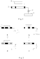
- the sensor includes a sensing component for detecting movement of an object to be detected 1.
- the sensing component comprises a first electrode layer 2 and a second electrode layer 3 associated therewith.
- the first electrode layer 2 and the second electrode layer 3 are separately disposed and electrically connected.
- the object to be detected 1 may be brought into contact with and then separation from the first electrode layer 2, as indicated by the arrow shown in Fig. 1 .
- the movement of the object to be detected 1 causes electric potential on the first electrode layer 2 generated by charges carried by the object to be detected 1 to change. Charges flow between the first electrode layer and the second electrode layer under the electrostatic induction effect to generate a current.
- a detection device 4 may be connected to detect a current in the sensing component, or a load may be connected such that power is supplied to the load by using the electrical energy generated by the sensor.
- a generator may be produced based on the above principle.
- the object to be detected mentioned in describing the above sensor is considered as a component that is included in the generator on its own. That is, the generator includes a first component 1 and a second component comprising a first electrode layer 2 and a second electrode layer 3 associated therewith.
- the first electrode layer 2 and the second electrode layer 3 are separately disposed and electrically connected to each other.
- the first component 1 may be brought into contact with and then separation from the first electrode layer 2, as indicated by the arrow shown in Fig. 1 .
- the movement of the first component 1 causes electric potential on the first electrode layer 2 generated by charges carried by the first component 1 to change. Charges flow between the first electrode layer and the second electrode layer under the electrostatic induction effect to generate a current.
- a detection device 4 may be connected to detect a current in the generator, or a load may be connected such that power is supplied to the load by using the electrical energy generated by the generator.
- the first component 1 is an uncharged object
- an embodiment in which the first component 1 is of insulator or semiconductor material and the first electrode layer 2 is of conductive material is taken as an example to specifically illustrate the operating principle of the generator. It should be noted that, since sensor and the generator according to the present disclosure have a similar structure, the operating principle of the generator is also suitable for the sensor.
- the above process shows that, when the above-described structure is used as a sensor and after the first component 1 that is used as the object to be detected is brought into contact with and then separation from the first electrode layer 2 in the sensing component, there is no need to provide an external power supply.
- the movement of the first component 1 that does not carry charges and that is used as the object to be detected may be detected by the sensing component of the sensor. If the first component 1 that is used as the object to be detected is brought into contact with and then separation from the sensing component of the sensor several times, several pulsed alternating current signals will be generated in the sensing component.
- the first component 1 may also be charged in advance prior to contacting the first electrode layer.
- the charges carried on the first component 1 will be redistributed between the first component and the first electrode layer. Due to different capabilities of different material to constrain charges, there is still difference in concentration of charge between two contact surfaces.
- the first component 1 and the first electrode layer 2 are separated from each other, the first component 1 still carries charges.
- the distance between the first component 1 and the first electrode layer 2 changes, charges flow between the first component 1 and the first electrode layer 2 due to the electrostatic induction effect and a current is output to the detecting device.
- Charges carried on the first component 1 may be obtained by charging it or by means of other manners. The method of obtaining the charges has no effect on the detecting process of the sensor and the process of generating electricity of the generator according to the present disclosure and will be not construed as a limitation to the sensor or generator according to the present disclosure.
- the first electrode layer 2 and material of the second electrode layer 3 may be same or different.
- the material of the first electrode layer 2 or the second electrode layer 3 may be selected from metal, indium tin oxide or organic conductor.
- the commonly used metal includes gold, silver, platinum, aluminum, nickel, copper, titanium, chromium, selenium, or alloy formed by the above metallic materials.
- the organic conductor generally includes conductive macromolecule, including self-polypyrrole, polyphenylene sulfide, polyphthalocyanine compounds, polyaniline and/or polythiophene.
- the quantity of the charges carried on the surface of the first component 1 is critical to the operation of the sensor or generator.
- material of the surface of the first component 1 that contacts with the first electrode layer 2 includes insulator material.
- the insulator material preferably includes polymer insulating material, which may particularly be chosen from: polytetrafluoroethylene, polydimethylsiloxane, polyimide, polydiphenyl propane carbonate, polyethylene glycol terephthalate, aniline-formaldehyde resin, polyformaldehyde, ethyl cellulose, polyamide, melamine-formaldehyde, polyethylene glycol succinate, cellulose, cellulose acetate, polyethylene glycol adipate, polydiallyl phthalate, regenerated cellulose sponge, polyurethane elastomer, styrene-propylene copolymer, styrene-butadiene copolymer, rayon, polymethacrylate, polyvinyl alcohol, polyester, polyisobutylene, polyurethane flexible sponge, polyethylene glycol terephthalate, polyvinyl butyral, phenolic resin, chloroprene rubber, butadiene-propylene
- insulating materials may also be used as material of the surface of the first component 1 that contacts with the first electrode layer 2, such as wool and fabrics thereof, silk and fabrics thereof, paper, cotton and fabrics thereof, polyurethane elastomer, wood, hard rubber, and acetate that is commonly used.
- the first electrode layer is of conductive material. Since there is a difference in electron donating and accepting capability between the semiconductor material and the conductive material, material of surface of the first component that may contact the first electrode layer may be selected from semiconductors, including silicon, germanium; a Group III and Group V compound, such as gallium arsenide, gallium phosphide; a Group II and Group VI compound, such as cadmium sulfide, zinc sulfide; and a solid solution consisting of a Group III-Group V compound and a Group II-Group VI compound, such as gallium aluminum arsenide, gallium arsenic phosphide,.
- semiconductors including silicon, germanium; a Group III and Group V compound, such as gallium arsenide, gallium phosphide; a Group II and Group VI compound, such as cadmium sulfide, zinc sulfide; and a solid solution consisting of a Group III-Group V compound and a Group II-Group VI compound, such
- Non-conductive oxides, semiconductor oxides, and complex oxides such as oxides of manganese, chromium, iron and copper, also including silicon oxide, manganese oxide, chromium oxide, iron oxides, copper oxide, zinc oxide, BiO 2 and Y 2 O 3 , also exhibit triboelectric characteristics and may generate surface charges in a friction process, thus they may also be used as the material of the first component in the present disclosure.
- the first component 1 In the sensor or generator, only the surface of the first component 1 and the surface of the first electrode layer 2 that can contact with each other have an influence on the output performance of the sensor or generator. It is only necessary to define the surface of the first component 1 that can contact with the first electrode layer 2 to be of the materials described above and the other portions of the first component 1 are not limited. Therefore, the first component 1 may entirely be made of homogeneous material, and may be a multilayer structure or a core-shell structure.
- the two surfaces by which the first component 1 and the first electrode layer 2 contact with each other may be of hard material or flexible material.
- the hardness of the material has no significant effect on the performance of generating electricity of the sensor or generator, and may extend the application scope of the sensor or generator according to the present disclosure.
- the quantity of the charges carried on the surface of the first component 1 has an effect on the output performance of the sensor or generator.
- the distance by which the first component 1 is spaced from the first electrode layer 2 of the second component also has an effect on the output performance of the sensor or generator. The greater the spaced distance is, the stronger the output signal from the sensor or generator is. It is found during a study that, when the spaced distance is greater than the size of the device, and particularly greater than the maximum length of the surfaces of the first component 1 and the first electrode layer 2 that contact with each other, change of the spaced distance has little effect on the output signal of the sensor or generator.
- the distance by which the first component 1 is spaced from the first electrode layer 2 is greater than 1 ⁇ m, more preferably from 1 ⁇ m to 10cm, and more preferably from 1mm to 2cm.
- the maximum length of the surface herein particularly refers to the maximum length of the surface in various directions, such as the length of the long side of a rectangle, the length of diameter of a circular surface. For the irregular surface, the maximum length of the surface may be determined by a specific measurement.
- the movement of the first component 1 relative to the second component may be implemented in various ways.
- the second component and particularlly the first electrode layer 2 of the second component is fixed.
- the first component 1 is fixed to a reciprocating component which drives the first component of the sensor or generator to reciprocate, achieving the contact-separation of the first component 1 relative to the second component.
- an elastic connector may also be provided between the first component 1 and the second electrode layer 2 to realize the purpose of reciprocating the first component 1 so as to approach or move away from the first electrode layer 2.
- the above purpose may be achieved by various technical means and conventional components for controlling distance in the art may be employed.
- the first component used as the object to be detected may be objects that are free to move, such as soles used when people walks.
- the first component 1 may be an object that is free to move and can be periodically brought into contact with and then separation from the first electrode layer.
- the first component 1 is fixed to other moving object and is used in conjunction with other products so as to drive the first component 1 to move relative to the first electrode layer 2 by means of the motion of other products, thereby achieving electricity generation of the generator.
- the first component 1 is an object that independently moves relative to the second component and there is no electrode layer connected thereto. Accordingly, the thickness, size and shape of the first component are not particularly limited.
- the first component 1 as a whole may be a block, plate, sheet or film.
- the surface of the first component 1 and the surface of the first electrode layer 2 that can contact with each other are substantially same, and preferably same with each other in shape and size.
- the surface of the first component 1 and the surface of the first electrode layer 2 that can contact with each other may be flat surfaces, or may be curved surfaces.
- the mutual contact thereof may also be achieved.
- the surface of the first component 1 and the surface of the first electrode layer 2 that can contact with each other are all flat or curved surface structure to ensure that a moment at which the contact area is maximum occurs when both of the two surfaces contact with each other.
- the surface of the first component 1 and the surface of the first electrode layer 2 that can contact with each other are curved surfaces with complementary shapes, such as curved surfaces with the same curvature and the same area, to ensure that the surface of the first component 1 and the surface of the first electrode layer 2 that can contact with each other may contact completely when contacting with each other.
- the shape of the surface of the first electrode layer 2 that contacts the object to be detected 1 may be flexibly selected to be either a flat surface or a curved surface.
- the surface of the object to be detected 1 and the surface of the first electrode layer 2 that can contact with each other are all curved surfaces, the mutual contact thereof may also be achieved.
- the surface of the object to be detected 1 and the surface of the first electrode layer 2 that can contact with each other are all flat or curved surface structure to ensure that a moment at which the contact area is maximum occurs when both of the two surfaces contact with each other.
- the surface of the object to be detected 1 and the surface of the first electrode layer 2 that can contact with each other are curved surfaces with complementary shapes, such as curved surfaces with the same curvature and the same area, to ensure that the surface of the object to be detected 1 and the surface of the first electrode layer 2 that can contact with each other may contact completely when contacting with each other.
- the sensing component and the object to be detected may also operate in an operating mode of sliding friction.
- Fig. 3 in which the sensing process is shown, a situation in which a lower surface of the object to be detected 11 and an upper surface of the first electrode layer 2 contact with each other is taken as an example of the sensing operating process.
- the lower surface of the object to be detected 11 and the upper surface of the first electrode layer 2 are same in shape and size. In practice, the lower surface of the object to be detected 11 and the upper surface of the first electrode layer 2 are not strictly limited to be same in shape and area.
- the lower surface of the object to be detected 11 may contact with the upper surface of the first electrode layer 2 or not. After they contact with each other under an effect of an external force F (see Fig. 3a ), since there is difference in triboelectric series between the material of the upper surface of the first electrode layer 2 and that of the lower surface of the object to be detected 11, there is a difference in electron donating and accepting capability therebetween.
- F an external force
- a situation in which the lower surface of the object to be detected 11 has a stronger electron accepting capability and the upper surface of the first electrode layer 2 is more susceptible to donate electrons is taken as an example.
- Surface charge transfer occurs when the lower surface of the object to be detected 11 contacts the upper surface of the first electrode layer 2.
- the upper surface of the first electrode layer 2 carries positive charges and the lower surface of the object to be detected 11 carries negative charges (as shown in Fig. 3a ). Since the two types of charges have the same electric quantity, there is no electric potential difference between the first electrode layer 2 and the second electrode layer 3 and thus there is no charge to flow.
- the surface of the first electrode layer 2 and the surface of the object to be detected 11 that may slidably contact with each other may be flat or curved surfaces.
- the surface of the first electrode layer 2 and the surface of the object to be detected 11 that may slidably contact with each other match in shape.
- the surface of the first electrode layer 2 and the surface of the object to be detected 11 that may slidably contact with each other are substantially same, preferably same, with each other in shape and size. A moment at which the contact area is largest occurs in the mutual sliding process.
- the surface of the first electrode layer 2 and the surface of the object to be detected 11 that may slidably contact with each other are arc surfaces with the same curvature.
- the surface of the first electrode layer 2 and the surface of the object to be detected 11 that may slidably contact with each other are smooth and flat surfaces, such a configuration requires a large relative-sliding space for the first electrode layer 2 and the object to be detected 11. Further, in a case that there is a large size difference between the surface of the first electrode layer 2 and the surface of the object to be detected 11 that may slidably contact with each other, a long sliding distance is necessary to meet the requirements for change of the contact area between the first electrode layer 2 and the object to be detected 11 and generation of an electrical signal in the process of mutual sliding friction.
- the surface of the first electrode layer 2 that can contact with the surface of the object to be detected 11 may be an uneven surface.
- the two surfaces incompletely contact.
- the surface of the first electrode layer 2 and the surface of the object to be detected 11 that can contact with each other are both uneven surfaces with a concave-convex structure.
- the present embodiment may be applicable in a case in which any one of the surface of the object to be detected 11 and the surface of the first electrode layer 2 that can contact with each other is small.
- the two surfaces contacting with each other are prepared to be uneven surfaces.
- the requirement for change of the contact area may be met within a small moving range when the surface of the first electrode layer 2 and the surface of the object to be detected 11 that contact with each other are brought into a friction relation to each other under the effect of the external force.
- the mechanical energy of the external force is converted into electrical energy, achieving the sensing of the movement of the object to be detected.
- the concavo-convex structures of the surface of the first electrode layer 2 and the surface of the object to be detected 11 that contact with each other are periodically concavo-convex structure.
- the periodically concavo-convex structure may be a periodic structure that includes strip structures arranged in an equidistant and parallel form, a chessboard structure, or the like.
- the surface of the first electrode layer and the surface of the object to be detected 11 that can contact may be treated by physical or chemical modification.
- the physical modification may be achieved by distributing a portion or all of surfaces with microstructure of micron or sub-micronmeter order to increase the contact area between the first electrode layer 2 and the object to be detected 11, thereby increasing the quantity of charge carried on the surface of the object to be detected.
- the microstructure is preferably nanowires, nanotubes, nanoparticles, nanorods, nanoflowers, nanogrooves, micron grooves, nanotapers, micron tapers, nanospheres, micron spherical structure or an array formed of one or more above structures, and in particular a nano array consisting of nanowires, nanotubes, nanotapers or nanorods, a linear, cubic or rectangular pyramid array that may be prepared with a method of photolithography, plasma etching, and the like.
- the size of each unit in the array is in the order of nanometer to micron.
- the specific size and shape of the micro and nano structures should not be a limitation to the scope of the disclosure. This purpose may also be achieved by points or a coating of nanomaterial.
- the surface of the first electrode layer may also be chemically modified such that the charge transfer quantity at the moment of contact may be further increased , thereby improving the contact charge concentration and output power of the sensor.
- the chemical modification may be divided into two following types:
- One type of method is: for the materials of the first electrode layer 2 and the object to be detected 11 that contact with each other, according to the polarities of the two types of materials, if the polarity of the material of the first electrode layer 2 is positive, to introduce a functional group that is susceptible to denote electrons (i.e., a strong electron-donating group) onto the material surface; or, if the polarity of the material of the first electrode layer 2 is negative, to introduce a functional group that is susceptible to accept electrons (i.e., a strong electron-accepting group) onto the material surface.
- the charge transfer quantity may be further increased at the moment of contacting or sliding relative to each other, thereby improving the charge concentration on the surface of the object to be detected and the sensing sensitivity.
- the strong electron-donating groups may include an amino group, a hydroxy group, an alkoxy group, and the like; and the strong electron-accepting groups may include an acyl group, a carboxyl group, a nitro group, a sulfonic acid group, and the like.
- the introduction of the functional groups may be carried out with a conventional method, such as plasma surface modification. For example, mixed gas of oxygen and nitrogen may generate plasma at a certain power, thereby introducing an amino group on the material surface.
- Another type of method is to introduce positive charges on the material surface the polarity of which is positive and to introduce negative charges on the material surface the polarity of which is negative.
- this may be achieved by way of chemical bonding.
- PDMS surface may be modified with tetraethyl orthosilicate (TEOS) with a sol-gel method so as to carry negative charges.
- TEOS tetraethyl orthosilicate
- a gold film layer may be modified by gold-sulfur bonding with gold nanoparticles the upper surface of which contains cetyl trimethyl ammonium bromide (CTAB). Since cetyl trimethyl ammonium bromide is cationic, the polarity of the whole material will be positive.
- CTAB cetyl trimethyl ammonium bromide
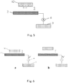
- the object to be detected in addition to the operating mode in which the object to be detected is brought into contact with and then separation from the sensing component and the operating mode in which the object to be detected and the sensing component slide relative to each other, in the case that the object to be detected carries charges itself, the object to be detected may move relative to the first electrode layer 2 of the sensing component. However, the object to be detected will not contact any electrode layer of the sensing component, as indicated by the arrow in Fig. 6 . It is provided that the object to be detected 12, and in particular the surface of the object to be detected 12 facing the first electrode layer 2 carries negative charges in advance.
- a detecting device 4 connected between the first electrode layer 2 and the second electrode layer 3 may detect a current that flows from the second electrode layer 3 to the first electrode layer 2, as shown in Fig. 6a .
- the repulsive effect of the negative charges carried by the object to be detected 12 to the negative charges in the first electrode layer 2 is reduced.
- a detecting device 4 connected between the first electrode layer and the second electrode layer may detect a current that flows from the first electrode layer 2 to the second electrode layer 3, as shown in Fig. 6b .
- the object to be detected 12 moves in a vertical direction relative to the first electrode layer, but the operating principle therein is also applicable to a situation in which the distance between the surface of the object to be detected 12 and the surface of the first electrode layer 2 that face towards each other does not change (i.e., the object to be detected 12 moves in a direction parallel to the first electrode layer).
- the sensing component may carry charges or may not carry charges. Even if the two electrode layers of the sensing component carry charges themselves, when the object to be detected 12 moves relative to the first electrode layer, the electric potential on the first electrode layer generated by the charges carried on the surface of the object to be detected 12 will change, thereby resulting in a charge flow between the first electrode layer and the second electrode layer.
- the charges carried by the object to be detected 12 may be obtained by frictionating the object to be detected 12 with other objects except the sensing component, may be obtained by frictionating the object to be detected 12 with the sensing component prior to operating, and may be obtained by other ways such as being charged.
- the way by which the charges are obtained has no effect on the sensing process in the present disclosure and will not constitute a limitation to the sensor of the present disclosure.
- the minimum distance between the first electrode layer 2 and the object to be detected 12 is 0.01 times the maximum length of the surface of the first electrode layer 2 that faces towards the object to be detected 12, and the maximum distance is 10 times the maximum length of the surface of the first electrode layer 2 that faces towards the object to be detected 12.
- the distance range between the object to be detected 12 and the first electrode layer 2 is 0.1-10 times the maximum length of the surface of the first electrode layer 2 that faces towards the object to be detected 12.
- the surface of the object to be detected 12 and the surface of the first electrode layer 2 that face towards each other are preferably substantially same, and, more preferbably, are same in shape and size, in order to ensure that the charges on the object to be detected may result in the charge flow between the first electrode layer 2 and the second electrode layer 3 under the effect of electrostatic induction, due to the movement of the object to be detected 12.
- the movement of the object to be detected relative to the first electrode layer may be a combination of three types of the above-mentioned relative movements, and is not limited to a single movement mode in which the object to be detected moves relative to the first electrode layer.
- the generator 11 includes a first component 11 and a second component, wherein the second component is same as that in the first embodiment and comprises the first electrode layer 2 and a second electrode layer 3 associated therewith.
- the first electrode layer 2 and the second electrode layer 3 are separately disposed and electrically connected.
- a surface of the first component 11 and the first electrode layer 2 of the second component may be brought into contact and then sliding friction with each other under the effect of external force F.
- the contact area changes in the sliding friction process.
- the relative sliding of the first component 11 relative to the first electrode layer 2 causes electric potential on the first electrode layer 2 generated by charges carried by the first component 11 to change.
- a detection device 4 may be connected to detect a current generated in the generator, or a load is connected such that power is supplied to the load by the electrical energy generated by the generator.
- the operating principle of the generator according to the present embodiment will be described in detail below in connection with the drawings.
- a situation in which the lower surface of the first component 11 and the upper surface of the first electrode layer 2 are in a contact and friction relation with each other is taken as an example.
- the lower surface of the first component 11 and the upper surface of the first electrode layer 2 are same in shape and size.
- the lower surface of the first component 11 and the upper surface of the first electrode layer 2 are not strictly limited to be same in shape and area. That is, they may be same or different in shape and area.
- the operating principle of the generator is shown in Fig. 3 . In an initial state, the lower surface of the first component 11 may be brought into contact with the upper surface of the first electrode layer 2 or not.
- various components of the generator may be same as those in the first embodiment in material and structure, which are omitted here.
- the surface of the first component 11 and the surface of the first electrode layer 2 that may slidably contact with each other may be flat or curved surfaces.
- the surface of the first component 11 and the surface of the first electrode layer 2 that may slidably contact with each other match in shape.
- the surface of the first component 11 and the surface of the first electrode layer 2 that may slidably contact with each other are substantially same, preferably, same, in shape and size. A moment at which the contact area is largest occurs in the mutual sliding process.
- the surface of the first component 11 and the surface of the first electrode layer 2 that may slidably contact with each other are arc surfaces with the same curvature.
- the surface of the first component 11 and the surface of the first electrode layer 2 that may slidably contact with each other are smooth and flat surfaces, such a configuration requires a large relative-sliding space for the first component 11 and the first electrode layer 2. Further, with respect to a case that there is a large size difference between the surface of the first component 11 and the surface of the first electrode layer 2 that may slidably contact with each other, the requirements in the process of mutual sliding friction between the first component 11 and the first electrode layer 2 for change of the contact area may not be met. Thus, in the generator of the present disclosure, the surface of the first component 11 and the surface of the first electrode layer 2 that can contact with each other may be uneven surfaces.
- the two surfaces incompletely contact.
- the surface of the first component 11 and the surface of the first electrode layer 2 that can contact with each other are both uneven surfaces with a concave-convex structure.
- the present embodiment is adaptable for a situation in which any surface of the surface of the first component 11 and the surface of the first electrode layer 2 that can contact with each other is small.
- the two surfaces contacting with each other are prepared to be uneven surfaces.
- the requirement for change of the contact area may be met within a small moving range when the surface of the first component 11 and the surface of the first electrode layer 2 that frictionate with each other under the effect of the external force. Then, the mechanical energy of the external force may be converted into electrical energy.
- the concavo-convex structures of the surface of the first component 11 and the surface of the first electrode layer 2 that contact with each other are periodically concavo-convex structure.
- the periodically concavo-convex structure may be a periodic structure that includes strip structures arranged in an equidistant and parallel form, a chessboard structure, or the like.
- the surface of the first component and the surface of the first electrode layer that can contact with each other may be treated by physical or chemical modification.
- the physical modification may be achieved by distributing a portion or all of surfaces with microstructure of micron or sub-micron order to increase the contact area between the first component 11 and the first electrode layer 2, thereby increasing the quantity of charge carried on the surface of the first component.
- the microstructure is preferably nanowires, nanotubes, nanoparticles, nanorods, nanoflowers, nanogrooves, micron grooves, nanotapers, micron tapers, nanospheres, micron spherical structure or an array formed of one or more above structures, and in particular a nano array consisting of nanowires, nanotubes, nanotapers or nanorods, a linear, cubic or rectangular pyramid array that may be prepared with a method of photolithography, plasma etching, and the like.
- the size of each unit in the array is in the order of nanometer to micron.
- the specific size and shape of the micro and nano structures should not be a limitation to the scope of the disclosure. This purpose may also be achieved by points or a coating of nanomaterial.
- the surface of the first component and/or the surface of the first electrode layer may also be chemically modified such that the charge transfer quantity at the moment of contact may be further increased, thereby improving the contact charge concentration and output power of the generator.
- the chemical modification may be divided into two
- Another type of method is to introduce positive charges on the material surface the polarity of which is positive and to introduce negative charges on the material surface the polarity of which is negative.
- this may be achieved by way of chemical bonding.
- PDMS surface may be modified with tetraethyl orthosilicate (TEOS) with a sol-gel method so as to carry negative charges.
- TEOS tetraethyl orthosilicate
- a gold film layer may be modified by gold-sulfur bonding with gold nanoparticles the upper surface of which contains cetyl trimethyl ammonium bromide (CTAB). Since cetyl trimethyl ammonium bromide is cationic, the polarity of the whole material will be positive.
- CTAB cetyl trimethyl ammonium bromide
- the first component is an object that may move independently from the second component. There is no need to provide an electrode for outputting electrical signal from the generator on the first component.
- the two electrodes for electrical connection are all disposed in the second component. According to the actual environment when used, the two electrode layers may be provided to be stationary and the distance or relative position therebetween may be easily provided according to the convenience for the external circuit connection, the operating environment, or the like, without consideration for the problem of movement of the electrode layer in the operating process of the generator. The defect that one electrode in the prior art generator should always move together with the moving first component may be prevented.
- the generator includes a first component 12 and a second component, wherein the second component comprises the first electrode layer 2 and a second electrode layer 3 associated therewith.
- the first electrode layer 2 and the second electrode layer 3 are separately disposed and electrically connected.
- the first component carries charges itself and may move relative to the first electrode layer 2 of the second component, as indicated by the arrow in Fig. 5 .
- the movement of the first component 12 causes electric potential on the first electrode layer 2 generated by charges carried by the first component 12 to change.
- the charges flow between the first electrode layer 2 and the second electrode layer 3 under the electrostatic induction effect to generate a current.
- a detection device 4 may be connected to detect a current generated in the generator, or a load is connected such that power is supplied to the load by the electrical energy generated by the generator.
- the operating process of the generator in the present embodiment is similar to that of the sensor in the first embodiment and reference may also be made to Fig. 6 .
- the first component 12 carries negative charges in advance, and in particular the surface of the first component 12 facing towards the first electrode layer 2 carries negative charges.
- a detecting device 4 connected between the first electrode layer 2 and the second electrode layer 3 may detect a current that flows from the second electrode layer 3 to the first electrode layer 2, as shown in Fig.
- a detecting device 4 connected between the first electrode layer and the second electrode layer may detect a current that flows from the first electrode layer 2 to the second electrode layer 3, as shown in Fig. 6b .
- the first component 12 moves in a vertical direction relative to the first electrode layer, but the operating principle thereof is also applicable to a situation in which the distance between the surface of the first component 12 and the surface of the first electrode layer 2 that face each other does not change (i.e., the first component 12 moves in a direction parallel to the first electrode layer).
- the second component may carry charges or may not carry charges. Even if the two electrode layers of the second component carry charges themselves, when the first component 12 moves relative to the first electrode layer, the electric potential on the first electrode layer generated by the charges carried on the surface of the first component 12 will change, thereby resulting in a charge flow between the first electrode layer and the second electrode layer.
- the charges carried by the first component 12 may be obtained by frictionating the first component 12 with other objects except the generator, may be obtained by frictionating the first component 12 with the generator's own second component, and may be obtained by other ways such as being charged.
- the way by which the charges are obtained has no effect on the electricity generating process in the present disclosure and will not constitute a limitation to the sensor of the present disclosure.
- the minimum distance between the first component 12 and the first electrode layer 2 is 0.01 times the maximum length of the surface of the first component 12 that faces towards the first electrode layer 2, and the maximum distance is 10 times the maximum length of the surface of the first component 12 that faces towards the first electrode layer 2.
- the distance range between the first component 12 and the first electrode layer 2 is 0.1-10 times the maximum length of the surface of the first component 12 that faces towards the first electrode layer 2.
- the projection of the first component on a plane in which the first electrode layer is located are preferably substantially same, and, more preferably, are same as the first electrode layer in shape and size, in order to ensure that the charges on the first component 12 may result in the charge flow between the first electrode layer 2 and the second electrode layer 3 under the effect of electrostatic induction, due to the movement of the first component 12.
- the material of the first component 12 may be selected from insulator materials and semiconductor materials, and preferably an electret material capable of "quasi-permanently" maintaining electrostatic charges, such as polytetrafluoroethylene, fluorinated ethylene propylene, quartz, perfluorinated cyclic polymer.
- the first component 12 may carry electrostatic charges by friction effect or other ways and maintain them for a long time.
- the insulator may be selected from some common organic polymeric materials and natural materials, including: polytetrafluoroethylene, polydimethylsiloxane, polyimide, polydiphenyl propane carbonate, polyethylene glycol terephthalate, aniline-formaldehyde resin, polyformaldehyde, ethyl cellulose, polyamide, melamine-formaldehyde, polyethylene glycol succinate, cellulose, cellulose acetate, polyethylene glycol adipate, polydiallyl phthalate, regenerated cellulose sponge, polyurethane elastomer, styrene-propylene copolymer, styrene-acrylonitrile copolymer, styrene-butadiene copolymer, polyamide nylon 11, polyamide nylon 66, wool and fabrics thereof, silk and fabrics thereof, paper, rayon, cotton and fabrics thereof, wood, hard rubber, polymethacrylate, polyvinyl alcohol, polyester, polyisobutylene
- Commonly used semiconductors include: silicon, germanium; a Group III and Group V compound, such as gallium arsenide, gallium phosphide; a Group II and Group VI compound, such as cadmium sulfide, zinc sulfide; and a solid solution consisting of a Group III-Group V compound and a Group II-Group VI compound, such as gallium aluminum arsenide, gallium arsenic phosphide.
- amorphous glass semiconductors, organic semiconductors, and the like are possible.
- Non-conductive oxides, semiconductor oxides, and complex oxides such as oxides of manganese, chromium, iron and copper, also including silicon oxide, manganese oxide, chromium oxide, iron oxides, copper oxide, zinc oxide, BiO 2 and Y 2 O 3 , may also be used as the material of the first component 12 in the present disclosure.
- the thickness thereof is not specially required and the material thereof may include a body material or may also be a film material, which causes the applicable scope of the generator according to the present disclosure to be greatly extended.
- the first component 12 of thin layer may be attached to a moving object and the relative movement of the first component 12 relative to the second component is controlled.
- the two electrode layers of the second component may be same as those in the first and second embodiments in material and structure and will not be repeatedly described here.
- the movement of the first component relative to the first electrode layer may be a combination of three types of the above-mentioned relative movements, and is not limited to a single movement mode in which the first component moves relative to the first electrode layer.
- the sensors or generators in the three above-described embodiments each may further include a friction layer.
- the first electrode layer of the sensing component (or the second component of the generator) is attached to the lower surface of the friction layer such that the first electrode layer will not directly contact other objects and the second component of the sensor or the generator may be protected.
- the friction layer of the sensor or the generator may carry charges or not. Since the relative position of the friction layer and the first electrode layer is constant, the friction layer will have no impact on the charge transfer between the first electrode layer and the second electrode layer of the second component when the first component carrying charges moves relative to the first electrode layer.
- the sensor or generator 13 includes: a first component 13; a second component that is formed by electrically connecting the first electrode layer 2 and the second electrode layer 3; and a friction layer 5 disposed on the upper surface of the first electrode layer 2, wherein the upper surface of the friction layer 5 faces towards the first component 13, and wherein the second component (or the sensing component) may be same as that in the previous embodiments.
- the first component 13 and the upper surface of the friction layer 5 may move relative to each other in a contact-separation manner such that the distance from the first component 13 to the first electrode layer changes.
- a sliding friction may occur between the first component 13 and the upper surface of the friction layer such that the contact area changes.
- the first component 13 may carry charges itself and will never contact the friction layer in the process of moving relative to the first electrode layer.
- the operating principle of the sensor or generator that includes a friction layer will be described below based on a moving mode in which the first component 13 and the upper surface of the friction layer move in a contact-separation manner. It is provided that the lower surface of the first component 13 and the upper surface of the friction layer 5 are of different materials and there is a difference in triboelectric series between the materials thereof.
- a structure shown in Fig. 7 is taken as an example to describe the operating principle of the sensor of generator according to the present embodiment below in detail. In an initial state, the first component 13 is not brought into contact with the friction layer 5 (see Fig. 7a ).
- the same principle is adaptive to a situation in which the first component may slidably contact the upper surface of the friction layer to change the contact area.
- the existence of the friction layer will not affect the operation of the sensor or the generator.
- the lower surface of the first component and the upper surface of the friction layer may be substantially same, and preferably same, in shape and size. Both of the surface of the first component and the surface of the friction surface that slide relative to each other may be smooth and flat surfaces.
- the upper surface of the friction layer is accordingly prepared to be a surface with a concave-convex structure.
- the first component may be not brought into contact with the friction layer, and at the same time not brought into contact with the second component (i.e., the first electrode layer or the second electrode layer). Since the relative position of the friction layer to the first electrode layer is fixed, the existence of the friction layer will not affect the charge transfer between the first electrode layer and the second electrode layer of the second component, as long as the first component carrying charges is controlled to be not brought into contact with the friction layer.
- the first component may be of a conductive material, such as metal or indium tin oxide ITO.
- a conductive material such as metal or indium tin oxide ITO.
- metals include gold, silver, platinum, aluminum, nickel, copper, titanium, chromium, or selenium, and alloys formed of the above-described metal.
- the upper surface of the friction layer may also be treated by physical or chemical modification, so that more charges may be generated on the surface of the first component when the friction layer contacts the first component.
- the charges carried by the first component itself may be obtained by frictionating the first component with other objects except the sensor or generator, may be obtained by frictionating the first component with the sensor or generator's own friction layer prior to operating, and may be obtained by other ways such as being charged.
- the material of the friction layer may be non-conductive material, and preferably an insulating material that may be selected from the optional material of the first component in the first embodiment.
- the existence of the friction layer may have a good protective effect for the first electrode layer 2, and thus the size and shape of the surface thereof is preferably at least completely cover the first electrode layer 2.
- the friction layer may further cover the second electrode layer 3.
- the thickness thereof should not be too large.
- the friction layer is preferably sheet-like or film-like, and the thickness thereof is generally chosen between 10nm and 5cm, preferably between 100nm and 5mm, and more preferably between 1 ⁇ m and 500 ⁇ m.
- the first electrode layer 2 is an electrode layer of the sensor or generator
- the first electrode layer is preferably prepared on the lower surface of the friction layer by using a conventional technology, such as magnetron sputtering, vapor deposition and printing.
- a thicker first electrode layer 2 may be employed, such as Cu or A1 foil, the surface of which is prepared with material of the friction layer 5, achieving a contact arrangement of the first electrode layer 2 with the friction layer 5.
- the friction layer may be a separate structure, for example consisting of two separate portions, one of which covers the surface of the first electrode layer 2 and the other of which covers the surface of the second electrode layer 3.
- the specific structure and shape of the friction layer may be arranged depending on the requirements of the first electrode layer of the sensor or generator, as long as the first electrode layer is protected from being worn without affecting the operation of the sensor or generator.
- the first component, the second component and the friction layer each may be of rigid or flexible material. Since the hardness of the material will not affect the sliding friction or contact friction effect therebetween, if a flat plane needs to be maintained by the surface of the first electrode layer or the first component, it may also be achieved through a support from the other components.
- the sensor or generator provided by the present disclosure may further include an isolating layer.
- the isolating layer is used to isolate the first electrode layer and the second electrode layer of the second component such that the first electrode layer and the second electrode layer are separated and are maintained in set relative positions and such that the second component may be insulated and isolated from other devices.
- the first electrode layer 2 and the second electrode layer 3 of the second component each are embedded in the isolating layer 6 such that the first electrode layer 2 and the second electrode layer 3 are isolated from each other and are maintained at a fixed relative position and such that at least the upper surface of the first electrode layer 2 may be exposed out of the isolating layer 6.
- the upper surface of the second electrode layer 3 may be exposed out of the isolating layer 6 or not.
- the first electrode layer 2 may be electrically connected to the second electrode layer 3 by a conductive wire or conductive film.
- the first electrode layer 2 and/or the second electrode layer 3 may be entirely wrapped by the isolating layer. Referring to Fig. 9 , all the surface of the first electrode layer 2 and the second electrode layer 3 are covered by the isolating layer 61. In the sensor or generator with such a structure, the isolating layer 61 covering the upper surface of the first electrode layer 2 further serves as the friction layer in the fourth embodiment.
- the first electrode layer 2 may be electrically connected to the second electrode layer 3 by a conductive wire or conductive film.
- the isolating layer and the two electrode layers of the second component are arranged in a stacked manner.
- the first electrode layer 2 and the second electrode layer 3 of the second component are disposed on upper and lower surfaces of the isolating layer 62, respectively, forming a multilayer structure.
- the first electrode layer 2 may be electrically connected to the second electrode layer 3 by a conductive wire or conductive film.
- the first electrode layer 2, the second electrode layer 3 and the isolating layer 62 each are of thin-layer structure, which may facilitate reduction of the overall structure of the sensor or generator and may miniaturize the device.
- the multilayer structure may include a friction layer 5 provided on the upper surface of the first electrode layer 2.
- the friction layer 5 may be brought into contact with and then separation from the first component 1 or into slidably friction with the first component 1 while protecting the first electrode layer, so that the surface of the first component 1 is charged.
- the multilayer structure may further include a protective layer 7 provided on the lower surface of the second electrode layer to protect the second electrode layer. This type of multilayer structure may be produced by a conventional preparation process for a semiconductor device.
- the first electrode layer 2 and the second electrode layer 3 each may be conductive film.
- Optional range for thickness of the film may be 10 nm-5 mm, preferably 100nm-500 ⁇ m.
- the first electrode layer 2 and the second electrode layer 3 is preferably a metal film layer, may be prepared on the upper and lower surfaces of the isolating layer 62 by using an existing technology, such as magnetron sputtering, vapor deposition and printing.
- they may be disposed on the upper and lower surfaces of the isolating layer 62 in a manner such as sticking.
- Material of the isolating layer and material of the protective layer is preferably of insulating material or semiconductor material. Since the isolating layer and the protective layer in the present disclosure is not involved in operating process of the sensor or generator, the material may be chosen in a wide range. All existing insulating material and semiconductor material may be chosen, such as organic insulator material PDMS, rubber or glass plate. The specific material may also be chosen from the insulating materials and the semiconductors enumerated in the first embodiment that may be employed by the first component.
- the isolating layer and the protective layer may be of rigid material or may be of flexible structure.
- the sensor or generator is called as flexible device that may be used in connection with other flexible devices.
- the sensor or generator made of flexible material is advantageous in that the friction surface that is soft, light and thin will be deformed when being subject to a slight external force. Such deformation will result in a relative displacement of the two friction material layers (first component 1 and the first electrode layer 2 or the friction layer 5), thereby outputting an electric signal out by the sliding friction.
- Use of flexible materials makes it possible for the sensor or generator according to the present disclosure may be widely used in biological and medical fields.
- macromolecule material that is ultra-thin, soft, flexible and/or transparent may be used as substrate and encapsulated to facilitate the use and to improve the strength. It is apparent that all the structures disclosed in the present disclosure each may be made of an appropriate super-soft elastic material, thereby forming a flexible sensor or generator.
- the first electrode layer 2 and the second electrode layer 3 are necessary to be electrically connected in order to generate a current between the first electrode layer 2 and the second electrode layer 3.
- the first electrode layer 2 may be electrically connected to the second electrode layer 3 directly by a load.
- the load may be a simple resistor (such as a lighting device) or a complex circuit (e.g. series-parallel circuit consisting of a plurality of electronic elements), and is not particularly limited here, as long as the first electrode layer 2 and the second electrode layer 3 may be electrically connected.
- the present disclosure further provides a sensing method that is applicable in any of the above-described sensors and provides a method of generating electricity that is applicable in any of the above-described generator, including steps of:
- the step of moving the first component 1 relative to the first electrode layer 2 may include: bringing the first component 1 into contact with a surface of the first electrode layer 2 and then separating it from the surface of the first electrode layer 2 such that the first component 1 is charged.
- electric potential on the first electrode layer generated by charges carried by the first component 1 changes, the electrostatic induction between the first component 1 and the first electrode layer 2 causes a current to flow through a load and the like, that is connected between the first electrode layer 2 and the second electrode layer 3.
- the step of moving the first component 1 relative to the first electrode layer 2 may include: bringing a surface of the first component 1 into sliding friction with a surface of the first electrode layer 2 to change contact area therebetween in the process of sliding friction, such that the surface of the first component 1 carries charges.
- electric potential on the first electrode layer 2 generated by charges carried by the first component 1 changes, the electrostatic induction between the first component 1 and the first electrode layer 2 causes a current to flow through a load and the like, that is connected between the first electrode layer 2 and the second electrode layer 3.
- the step of moving the first component 1 relative to the first electrode layer 2 may include: moving the first component 1 relative to the first electrode layer 2 without contacting the first electrode layer 2 at any time in a case that the first component 1 carries charges itself.
- electric potential on the first electrode layer 2 generated by charges carried by the first component 1 changes, the electrostatic induction between the first component 1 and the first electrode layer 2 causes a current to flow through a load and the like, that is connected between the first electrode layer 2 and the second electrode layer 3.
- the charges carried by the first component may be obtained after the first component and the first electrode layer 2 are brought into contact and then separation from each other and may also be obtained in other ways.
- the material and structure of the first component as well as the first electrode layer and the second electrode layer of the second component may adopt those of respective components in the above-mentioned sensor or generator in the present disclosure and will not be repeatedly described here.
- a thin plate of polymethyl methacrylate with a length of 10 cm ⁇ a width of 10 cm ⁇ a thickness of 1mm is obtained to serve as a substrate by cutting.
- a copper film is deposited on one side of the polyimide thin plate to serve as the first electrode layer and another copper film is deposited on the other side thereof to serve as the second electrode layer.
- the copper films are connected with a copper wire and a voltmeter is introduced.
- a layer of polytetrafluoroethylene film with a length of 10 cm ⁇ a width of 10 cm ⁇ a thickness of 75 ⁇ m is adhered to the surface of the first electrode layer to serve as the friction layer.
- a layer of nylon film with a length of 10 cm ⁇ a width of 10 cm ⁇ a thickness of 50 ⁇ m is adhered to the surface of the second electrode layer to serve as a protective layer.
- the polytetrafluoroethylene film is placed on the ground upwards and a sole is brought into contact with and then separation from it periodically.
- a maximum value of the voltage signal between the two copper films measured by a voltmeter is about 650V, showing that the sensor is capable of sensing a moving object.
- the movement of an object may be sensed by converting the mechanical energy from the external force into electrical energy without supplying an additional power supply to the sensor.
- When used as a generator it is possible to convert the mechanical energy from the external force into electrical energy to generate electricity.
- the present embodiment provides a process for preparing a specific generator.
- An organic glass sheet with a length of 10 cm ⁇ a width of 2 cm ⁇ a thickness of 1.59 mm is obtained to serve as the isolating layer of the generator with a laser by cutting.
- an aluminum film with a thickness of 1 ⁇ m is deposited on the upper surface of the isolating layer to serve as the first electrode layer and an aluminum foil with a length of 10 cm ⁇ a width of 2 cm ⁇ a thickness of 25 ⁇ m is deposited on the lower surface to serve as the second electrode layer.
- the first electrode layer and the second electrode layer are electrically connected with a LED lamp.
- a nanowire coating of polytetrafluoroethylene is prepared on the upper surface of the polytetrafluoroethylene film with a length of 10 cm ⁇ a width of 2 cm ⁇ a thickness of 50 ⁇ m to serve as the friction layer.
- the lower surface of the polytetrafluoroethylene film is adhered to the upper surface of the first electrode layer by conductive glue.
- a aluminum sheet with a length of 10 cm ⁇ a width of 2 cm ⁇ a thickness of 2 mm serves as the first component.
- the surface of the aluminum sheet and the surface of the polytetrafluoroethylene film is provided in a stacked manner each other.
- the aluminum sheet slides relative to the polytetrafluoroethylene film under the effect of external force and the contact area changes.
- the LED lamp connected between the first electrode layer and the second electrode layer may be lighted. It is shown that the generator can convert the mechanical energy from the external force into electrical energy to generate electricity.
Landscapes
- Physics & Mathematics (AREA)
- Spectroscopy & Molecular Physics (AREA)
- Chemical & Material Sciences (AREA)
- General Physics & Mathematics (AREA)
- Chemical Kinetics & Catalysis (AREA)
- Inorganic Chemistry (AREA)
- Engineering & Computer Science (AREA)
- Ceramic Engineering (AREA)
- Power Engineering (AREA)
- Other Investigation Or Analysis Of Materials By Electrical Means (AREA)
- Geophysics And Detection Of Objects (AREA)
- Measurement Of Length, Angles, Or The Like Using Electric Or Magnetic Means (AREA)
Applications Claiming Priority (3)
| Application Number | Priority Date | Filing Date | Title |
|---|---|---|---|
| CN201410157925.7A CN105099256B (zh) | 2014-04-18 | 2014-04-18 | 基于静电感应的发电机和发电方法 |
| CN201410158431.0A CN105091913B (zh) | 2014-04-18 | 2014-04-18 | 基于静电感应的传感器和传感方法 |
| PCT/CN2015/076872 WO2015158302A1 (fr) | 2014-04-18 | 2015-04-17 | Capteur et générateur d'énergie à base d'induction électrostatique, procédé de détection et procédé de génération d'énergie |
Publications (3)
| Publication Number | Publication Date |
|---|---|
| EP3133375A1 true EP3133375A1 (fr) | 2017-02-22 |
| EP3133375A4 EP3133375A4 (fr) | 2018-04-04 |
| EP3133375B1 EP3133375B1 (fr) | 2021-09-15 |
Family
ID=54323506
Family Applications (1)
| Application Number | Title | Priority Date | Filing Date |
|---|---|---|---|
| EP15779244.1A Active EP3133375B1 (fr) | 2014-04-18 | 2015-04-17 | Capteur et générateur d'énergie à base d'induction électrostatique, procédé de détection et procédé de génération d'énergie |
Country Status (4)
| Country | Link |
|---|---|
| EP (1) | EP3133375B1 (fr) |
| JP (1) | JP6581181B2 (fr) |
| KR (1) | KR101939607B1 (fr) |
| WO (1) | WO2015158302A1 (fr) |
Cited By (1)
| Publication number | Priority date | Publication date | Assignee | Title |
|---|---|---|---|---|
| WO2019182432A1 (fr) * | 2018-03-21 | 2019-09-26 | Fernandez Del Castillo Y Simon Gustavo | Éliminateur de charges électrostatiques pour des personnes |
Families Citing this family (9)
| Publication number | Priority date | Publication date | Assignee | Title |
|---|---|---|---|---|
| CN111104659B (zh) * | 2018-10-26 | 2024-06-14 | 北京纳米能源与系统研究所 | 用于智能识别的薄膜及智能识别系统 |
| CN109470133B (zh) * | 2018-11-05 | 2019-09-06 | 浙江大学 | 静电式自供能应变栅格传感器 |
| KR102259054B1 (ko) | 2019-09-02 | 2021-05-31 | 중앙대학교 산학협력단 | 마찰대전 및 전계방출에 의한 에너지 수확을 가능하게 하는 정전 소자 |
| WO2021081748A1 (fr) * | 2019-10-29 | 2021-05-06 | 浙江大学 | Capteur autonome pouvant être utilisé pour tester en temps réel une résistance latérale et une résistance d'extrémité d'un pieu de tuyau marin et dispositif de test |
| CN111808543B (zh) * | 2020-06-24 | 2021-08-10 | 浙江大学 | 一种基于摩擦生电的结构变形监测胶带 |
| KR102575879B1 (ko) * | 2020-08-28 | 2023-09-06 | 서울대학교산학협력단 | 정전 유닛, 이를 포함하는 다기능 정전 접착장치 및 정전 유닛의 제조방법 |
| KR102857921B1 (ko) * | 2022-12-07 | 2025-09-10 | 한국기술교육대학교 산학협력단 | 가소제를 포함하는 마찰대전 에너지 하베스터용 고분자 겔 및 이를 포함하는 마찰대전 에너지 하베스터 |
| CN116295634B (zh) * | 2023-03-01 | 2026-04-21 | 济南大学 | 一种柔性多功能传感器、系统及制备方法 |
| CN116480229B (zh) * | 2023-05-17 | 2026-03-03 | 江苏大学 | 一种非物理接触的多维信息融合智能手势密码锁 |
Family Cites Families (29)
| Publication number | Priority date | Publication date | Assignee | Title |
|---|---|---|---|---|
| JP4212865B2 (ja) * | 2002-10-11 | 2009-01-21 | アルプス電気株式会社 | 静電容量式センサ |
| JP2005221472A (ja) * | 2004-02-09 | 2005-08-18 | Olympus Corp | 静電型エンコーダ及び静電型変位測定方法 |
| EP1801600A1 (fr) * | 2005-12-23 | 2007-06-27 | The European Community, represented by the European Commission | Capteur électrostatique |
| US20100019616A1 (en) * | 2006-08-31 | 2010-01-28 | Sanyo Electric Co., Ltd. | Electrostatic operation device |
| US8283834B2 (en) * | 2007-10-25 | 2012-10-09 | Sanyo Electric Co., Ltd. | Power generating apparatus having ball bearings |
| JP2009207344A (ja) * | 2008-02-28 | 2009-09-10 | Tohoku Univ | エレクトレット機械電気エネルギー変換装置およびその製造方法 |
| JP5434305B2 (ja) * | 2009-06-30 | 2014-03-05 | トヨタ紡織株式会社 | 発電マット |
| JP5402395B2 (ja) * | 2009-08-21 | 2014-01-29 | オムロン株式会社 | 静電誘導型発電装置 |
| WO2011052106A1 (fr) * | 2009-10-29 | 2011-05-05 | パナソニック株式会社 | Générateur d'énergie |
| JP2011165519A (ja) * | 2010-02-10 | 2011-08-25 | Toshiba Corp | 静電型アクチュエータの駆動方法、及び静電型アクチュエータ装置 |
| JP2011172367A (ja) * | 2010-02-17 | 2011-09-01 | Toyota Boshoku Corp | 発電マット |
| JP5521159B2 (ja) * | 2010-03-04 | 2014-06-11 | 独立行政法人科学技術振興機構 | エレクトレット、静電誘導型変換素子及びエレクトレットの荷電方法 |
| KR101819780B1 (ko) * | 2010-12-03 | 2018-01-17 | 아사히 가라스 가부시키가이샤 | 전하 유지 매체의 제조 방법 |
| JP5702125B2 (ja) * | 2010-12-03 | 2015-04-15 | 富士フイルム株式会社 | 静電誘導型変換素子 |
| US9178446B2 (en) * | 2011-08-30 | 2015-11-03 | Georgia Tech Research Corporation | Triboelectric generator |
| JP5945102B2 (ja) * | 2011-09-01 | 2016-07-05 | 学校法人 関西大学 | 発電装置 |
| JP2013188080A (ja) * | 2012-03-09 | 2013-09-19 | Panasonic Corp | 振動発電器 |
| JP5994347B2 (ja) * | 2012-04-09 | 2016-09-21 | 日油株式会社 | 起電フィルムと発電装置 |
| CN102710166B (zh) * | 2012-04-13 | 2015-01-07 | 纳米新能源(唐山)有限责任公司 | 一种摩擦发电机 |
| CN202856656U (zh) * | 2012-05-15 | 2013-04-03 | 纳米新能源(唐山)有限责任公司 | 一种摩擦发电机以及摩擦发电机机组 |
| JP5790601B2 (ja) * | 2012-07-19 | 2015-10-07 | オムロン株式会社 | 振動発電装置 |
| JP5480414B2 (ja) * | 2012-07-25 | 2014-04-23 | 株式会社ビスキャス | 振動発電ケーブル、その製造方法、および振動発電体 |
| CN103368447B (zh) * | 2012-08-13 | 2016-02-03 | 北京纳米能源与系统研究所 | 静电脉冲发电机和直流脉冲发电机 |
| CN103684035B (zh) * | 2012-09-20 | 2015-09-30 | 纳米新能源(唐山)有限责任公司 | 多层高功率纳米摩擦发电机 |
| CN202818150U (zh) * | 2012-09-20 | 2013-03-20 | 纳米新能源(唐山)有限责任公司 | 纳米摩擦发电机 |
| CN103368452B (zh) * | 2013-03-08 | 2016-03-30 | 北京纳米能源与系统研究所 | 静电脉冲发电机和直流脉冲发电机 |
| CN103354429B (zh) * | 2013-03-12 | 2015-09-16 | 北京纳米能源与系统研究所 | 一种滑动摩擦纳米发电机及发电方法 |
| CN203532171U (zh) * | 2013-05-31 | 2014-04-09 | 纳米新能源(唐山)有限责任公司 | 风力发电装置及风力发电系统 |
| CN104734556B (zh) * | 2013-12-23 | 2017-01-25 | 北京纳米能源与系统研究所 | 一种非接触式静电感应纳米发电机、发电机组和发电方法 |
-
2015
- 2015-04-17 WO PCT/CN2015/076872 patent/WO2015158302A1/fr not_active Ceased
- 2015-04-17 EP EP15779244.1A patent/EP3133375B1/fr active Active
- 2015-04-17 KR KR1020167032262A patent/KR101939607B1/ko active Active
- 2015-04-17 JP JP2017505698A patent/JP6581181B2/ja active Active
Cited By (1)
| Publication number | Priority date | Publication date | Assignee | Title |
|---|---|---|---|---|
| WO2019182432A1 (fr) * | 2018-03-21 | 2019-09-26 | Fernandez Del Castillo Y Simon Gustavo | Éliminateur de charges électrostatiques pour des personnes |
Also Published As
| Publication number | Publication date |
|---|---|
| WO2015158302A1 (fr) | 2015-10-22 |
| KR20160146876A (ko) | 2016-12-21 |
| EP3133375B1 (fr) | 2021-09-15 |
| EP3133375A4 (fr) | 2018-04-04 |
| JP2017518512A (ja) | 2017-07-06 |
| KR101939607B1 (ko) | 2019-01-17 |
| JP6581181B2 (ja) | 2019-09-25 |
Similar Documents
| Publication | Publication Date | Title |
|---|---|---|
| EP3133375B1 (fr) | Capteur et générateur d'énergie à base d'induction électrostatique, procédé de détection et procédé de génération d'énergie | |
| CN105091913B (zh) | 基于静电感应的传感器和传感方法 | |
| JP6356791B2 (ja) | スライド摩擦式発電機、発電方法及びベクトル変位センサ | |
| CN105099256B (zh) | 基于静电感应的发电机和发电方法 | |
| CN104253561B (zh) | 滑动摩擦发电机、发电方法以及矢量位移传感器 | |
| KR101982691B1 (ko) | 슬라이드 마찰식 나노발전기 및 발전 방법 | |
| CN104748769B (zh) | 一种基于静电感应的传感器以及传感方法 | |
| CN104682766B (zh) | 基于独立摩擦层的纳米发电机、发电机组和发电方法 | |
| JP6510429B2 (ja) | スライド摩擦式ナノ発電機および発電方法 | |
| CN103795288B (zh) | 一种转动式静电发电装置 | |
| KR101928088B1 (ko) | 단극 마찰식 나노발전기, 발전 방법 및 자체 구동 추적 장치 | |
| CN110572073B (zh) | 一种混合型摩擦纳米发电机 | |
| CN104682767B (zh) | 基于单电极的旋转式摩擦电纳米发电机和流体流速传感器 | |
| CN105099260B (zh) | 基于流动液体的复合式发电机、发电方法和传感方法 | |
| CN104734556B (zh) | 一种非接触式静电感应纳米发电机、发电机组和发电方法 | |
| CN104868778B (zh) | 一种自驱动瞬态应力传感装置 | |
| CN104253562B (zh) | 包围式单电极摩擦纳米发电机、发电方法和追踪装置 | |
| CN110138261A (zh) | 一种基于双电荷层的发电机及其发电方法 |
Legal Events
| Date | Code | Title | Description |
|---|---|---|---|
| STAA | Information on the status of an ep patent application or granted ep patent |
Free format text: STATUS: THE INTERNATIONAL PUBLICATION HAS BEEN MADE |
|
| PUAI | Public reference made under article 153(3) epc to a published international application that has entered the european phase |
Free format text: ORIGINAL CODE: 0009012 |
|
| STAA | Information on the status of an ep patent application or granted ep patent |
Free format text: STATUS: REQUEST FOR EXAMINATION WAS MADE |
|
| 17P | Request for examination filed |
Effective date: 20161118 |
|
| AK | Designated contracting states |
Kind code of ref document: A1 Designated state(s): AL AT BE BG CH CY CZ DE DK EE ES FI FR GB GR HR HU IE IS IT LI LT LU LV MC MK MT NL NO PL PT RO RS SE SI SK SM TR |
|
| AX | Request for extension of the european patent |
Extension state: BA ME |
|
| DAV | Request for validation of the european patent (deleted) | ||
| DAX | Request for extension of the european patent (deleted) | ||
| RIC1 | Information provided on ipc code assigned before grant |
Ipc: G01D 5/24 20060101ALI20171103BHEP Ipc: G01P 13/00 20060101ALI20171103BHEP Ipc: H02N 1/04 20060101ALI20171103BHEP Ipc: G01D 5/14 20060101AFI20171103BHEP |
|
| REG | Reference to a national code |
Ref country code: DE Ref legal event code: R079 Ref document number: 602015073343 Country of ref document: DE Free format text: PREVIOUS MAIN CLASS: G01D0005140000 Ipc: G01D0005240000 |
|
| A4 | Supplementary search report drawn up and despatched |
Effective date: 20180302 |
|
| RIC1 | Information provided on ipc code assigned before grant |
Ipc: H02N 1/08 20060101ALI20180226BHEP Ipc: G01D 5/24 20060101AFI20180226BHEP |
|
| STAA | Information on the status of an ep patent application or granted ep patent |
Free format text: STATUS: EXAMINATION IS IN PROGRESS |
|
| 17Q | First examination report despatched |
Effective date: 20190624 |
|
| GRAP | Despatch of communication of intention to grant a patent |
Free format text: ORIGINAL CODE: EPIDOSNIGR1 |
|
| STAA | Information on the status of an ep patent application or granted ep patent |
Free format text: STATUS: GRANT OF PATENT IS INTENDED |
|
| INTG | Intention to grant announced |
Effective date: 20210504 |
|
| GRAS | Grant fee paid |
Free format text: ORIGINAL CODE: EPIDOSNIGR3 |
|
| GRAA | (expected) grant |
Free format text: ORIGINAL CODE: 0009210 |
|
| STAA | Information on the status of an ep patent application or granted ep patent |
Free format text: STATUS: THE PATENT HAS BEEN GRANTED |
|
| AK | Designated contracting states |
Kind code of ref document: B1 Designated state(s): AL AT BE BG CH CY CZ DE DK EE ES FI FR GB GR HR HU IE IS IT LI LT LU LV MC MK MT NL NO PL PT RO RS SE SI SK SM TR |
|
| REG | Reference to a national code |
Ref country code: GB Ref legal event code: FG4D Ref country code: CH Ref legal event code: EP |
|
| REG | Reference to a national code |
Ref country code: DE Ref legal event code: R096 Ref document number: 602015073343 Country of ref document: DE |
|
| REG | Reference to a national code |
Ref country code: IE Ref legal event code: FG4D |
|
| REG | Reference to a national code |
Ref country code: AT Ref legal event code: REF Ref document number: 1430836 Country of ref document: AT Kind code of ref document: T Effective date: 20211015 |
|
| REG | Reference to a national code |
Ref country code: LT Ref legal event code: MG9D |
|
| REG | Reference to a national code |
Ref country code: NL Ref legal event code: MP Effective date: 20210915 |
|
| PG25 | Lapsed in a contracting state [announced via postgrant information from national office to epo] |
Ref country code: HR Free format text: LAPSE BECAUSE OF FAILURE TO SUBMIT A TRANSLATION OF THE DESCRIPTION OR TO PAY THE FEE WITHIN THE PRESCRIBED TIME-LIMIT Effective date: 20210915 Ref country code: RS Free format text: LAPSE BECAUSE OF FAILURE TO SUBMIT A TRANSLATION OF THE DESCRIPTION OR TO PAY THE FEE WITHIN THE PRESCRIBED TIME-LIMIT Effective date: 20210915 Ref country code: SE Free format text: LAPSE BECAUSE OF FAILURE TO SUBMIT A TRANSLATION OF THE DESCRIPTION OR TO PAY THE FEE WITHIN THE PRESCRIBED TIME-LIMIT Effective date: 20210915 Ref country code: NO Free format text: LAPSE BECAUSE OF FAILURE TO SUBMIT A TRANSLATION OF THE DESCRIPTION OR TO PAY THE FEE WITHIN THE PRESCRIBED TIME-LIMIT Effective date: 20211215 Ref country code: FI Free format text: LAPSE BECAUSE OF FAILURE TO SUBMIT A TRANSLATION OF THE DESCRIPTION OR TO PAY THE FEE WITHIN THE PRESCRIBED TIME-LIMIT Effective date: 20210915 Ref country code: BG Free format text: LAPSE BECAUSE OF FAILURE TO SUBMIT A TRANSLATION OF THE DESCRIPTION OR TO PAY THE FEE WITHIN THE PRESCRIBED TIME-LIMIT Effective date: 20211215 Ref country code: LT Free format text: LAPSE BECAUSE OF FAILURE TO SUBMIT A TRANSLATION OF THE DESCRIPTION OR TO PAY THE FEE WITHIN THE PRESCRIBED TIME-LIMIT Effective date: 20210915 |
|
| REG | Reference to a national code |
Ref country code: AT Ref legal event code: MK05 Ref document number: 1430836 Country of ref document: AT Kind code of ref document: T Effective date: 20210915 |
|
| PG25 | Lapsed in a contracting state [announced via postgrant information from national office to epo] |
Ref country code: LV Free format text: LAPSE BECAUSE OF FAILURE TO SUBMIT A TRANSLATION OF THE DESCRIPTION OR TO PAY THE FEE WITHIN THE PRESCRIBED TIME-LIMIT Effective date: 20210915 Ref country code: GR Free format text: LAPSE BECAUSE OF FAILURE TO SUBMIT A TRANSLATION OF THE DESCRIPTION OR TO PAY THE FEE WITHIN THE PRESCRIBED TIME-LIMIT Effective date: 20211216 |
|
| PG25 | Lapsed in a contracting state [announced via postgrant information from national office to epo] |
Ref country code: AT Free format text: LAPSE BECAUSE OF FAILURE TO SUBMIT A TRANSLATION OF THE DESCRIPTION OR TO PAY THE FEE WITHIN THE PRESCRIBED TIME-LIMIT Effective date: 20210915 |
|
| PG25 | Lapsed in a contracting state [announced via postgrant information from national office to epo] |
Ref country code: IS Free format text: LAPSE BECAUSE OF FAILURE TO SUBMIT A TRANSLATION OF THE DESCRIPTION OR TO PAY THE FEE WITHIN THE PRESCRIBED TIME-LIMIT Effective date: 20220115 Ref country code: SM Free format text: LAPSE BECAUSE OF FAILURE TO SUBMIT A TRANSLATION OF THE DESCRIPTION OR TO PAY THE FEE WITHIN THE PRESCRIBED TIME-LIMIT Effective date: 20210915 Ref country code: SK Free format text: LAPSE BECAUSE OF FAILURE TO SUBMIT A TRANSLATION OF THE DESCRIPTION OR TO PAY THE FEE WITHIN THE PRESCRIBED TIME-LIMIT Effective date: 20210915 Ref country code: RO Free format text: LAPSE BECAUSE OF FAILURE TO SUBMIT A TRANSLATION OF THE DESCRIPTION OR TO PAY THE FEE WITHIN THE PRESCRIBED TIME-LIMIT Effective date: 20210915 Ref country code: PT Free format text: LAPSE BECAUSE OF FAILURE TO SUBMIT A TRANSLATION OF THE DESCRIPTION OR TO PAY THE FEE WITHIN THE PRESCRIBED TIME-LIMIT Effective date: 20220117 Ref country code: PL Free format text: LAPSE BECAUSE OF FAILURE TO SUBMIT A TRANSLATION OF THE DESCRIPTION OR TO PAY THE FEE WITHIN THE PRESCRIBED TIME-LIMIT Effective date: 20210915 Ref country code: NL Free format text: LAPSE BECAUSE OF FAILURE TO SUBMIT A TRANSLATION OF THE DESCRIPTION OR TO PAY THE FEE WITHIN THE PRESCRIBED TIME-LIMIT Effective date: 20210915 Ref country code: ES Free format text: LAPSE BECAUSE OF FAILURE TO SUBMIT A TRANSLATION OF THE DESCRIPTION OR TO PAY THE FEE WITHIN THE PRESCRIBED TIME-LIMIT Effective date: 20210915 Ref country code: EE Free format text: LAPSE BECAUSE OF FAILURE TO SUBMIT A TRANSLATION OF THE DESCRIPTION OR TO PAY THE FEE WITHIN THE PRESCRIBED TIME-LIMIT Effective date: 20210915 Ref country code: CZ Free format text: LAPSE BECAUSE OF FAILURE TO SUBMIT A TRANSLATION OF THE DESCRIPTION OR TO PAY THE FEE WITHIN THE PRESCRIBED TIME-LIMIT Effective date: 20210915 Ref country code: AL Free format text: LAPSE BECAUSE OF FAILURE TO SUBMIT A TRANSLATION OF THE DESCRIPTION OR TO PAY THE FEE WITHIN THE PRESCRIBED TIME-LIMIT Effective date: 20210915 |
|
| REG | Reference to a national code |
Ref country code: DE Ref legal event code: R097 Ref document number: 602015073343 Country of ref document: DE |
|
| PLBE | No opposition filed within time limit |
Free format text: ORIGINAL CODE: 0009261 |
|
| STAA | Information on the status of an ep patent application or granted ep patent |
Free format text: STATUS: NO OPPOSITION FILED WITHIN TIME LIMIT |
|
| PG25 | Lapsed in a contracting state [announced via postgrant information from national office to epo] |
Ref country code: DK Free format text: LAPSE BECAUSE OF FAILURE TO SUBMIT A TRANSLATION OF THE DESCRIPTION OR TO PAY THE FEE WITHIN THE PRESCRIBED TIME-LIMIT Effective date: 20210915 |
|
| 26N | No opposition filed |
Effective date: 20220616 |
|
| PG25 | Lapsed in a contracting state [announced via postgrant information from national office to epo] |
Ref country code: SI Free format text: LAPSE BECAUSE OF FAILURE TO SUBMIT A TRANSLATION OF THE DESCRIPTION OR TO PAY THE FEE WITHIN THE PRESCRIBED TIME-LIMIT Effective date: 20210915 |
|
| REG | Reference to a national code |
Ref country code: CH Ref legal event code: PL |
|
| REG | Reference to a national code |
Ref country code: BE Ref legal event code: MM Effective date: 20220430 |
|
| PG25 | Lapsed in a contracting state [announced via postgrant information from national office to epo] |
Ref country code: MC Free format text: LAPSE BECAUSE OF FAILURE TO SUBMIT A TRANSLATION OF THE DESCRIPTION OR TO PAY THE FEE WITHIN THE PRESCRIBED TIME-LIMIT Effective date: 20210915 Ref country code: LU Free format text: LAPSE BECAUSE OF NON-PAYMENT OF DUE FEES Effective date: 20220417 Ref country code: LI Free format text: LAPSE BECAUSE OF NON-PAYMENT OF DUE FEES Effective date: 20220430 Ref country code: IT Free format text: LAPSE BECAUSE OF FAILURE TO SUBMIT A TRANSLATION OF THE DESCRIPTION OR TO PAY THE FEE WITHIN THE PRESCRIBED TIME-LIMIT Effective date: 20210915 Ref country code: CH Free format text: LAPSE BECAUSE OF NON-PAYMENT OF DUE FEES Effective date: 20220430 |
|
| PG25 | Lapsed in a contracting state [announced via postgrant information from national office to epo] |
Ref country code: BE Free format text: LAPSE BECAUSE OF NON-PAYMENT OF DUE FEES Effective date: 20220430 |
|
| PG25 | Lapsed in a contracting state [announced via postgrant information from national office to epo] |
Ref country code: IE Free format text: LAPSE BECAUSE OF NON-PAYMENT OF DUE FEES Effective date: 20220417 |
|
| PG25 | Lapsed in a contracting state [announced via postgrant information from national office to epo] |
Ref country code: HU Free format text: LAPSE BECAUSE OF FAILURE TO SUBMIT A TRANSLATION OF THE DESCRIPTION OR TO PAY THE FEE WITHIN THE PRESCRIBED TIME-LIMIT; INVALID AB INITIO Effective date: 20150417 |
|
| PG25 | Lapsed in a contracting state [announced via postgrant information from national office to epo] |
Ref country code: MK Free format text: LAPSE BECAUSE OF FAILURE TO SUBMIT A TRANSLATION OF THE DESCRIPTION OR TO PAY THE FEE WITHIN THE PRESCRIBED TIME-LIMIT Effective date: 20210915 Ref country code: CY Free format text: LAPSE BECAUSE OF FAILURE TO SUBMIT A TRANSLATION OF THE DESCRIPTION OR TO PAY THE FEE WITHIN THE PRESCRIBED TIME-LIMIT Effective date: 20210915 |
|
| PG25 | Lapsed in a contracting state [announced via postgrant information from national office to epo] |
Ref country code: MT Free format text: LAPSE BECAUSE OF FAILURE TO SUBMIT A TRANSLATION OF THE DESCRIPTION OR TO PAY THE FEE WITHIN THE PRESCRIBED TIME-LIMIT Effective date: 20210915 |
|
| PGFP | Annual fee paid to national office [announced via postgrant information from national office to epo] |
Ref country code: DE Payment date: 20250422 Year of fee payment: 11 |
|
| PGFP | Annual fee paid to national office [announced via postgrant information from national office to epo] |
Ref country code: FR Payment date: 20250425 Year of fee payment: 11 |
|
| PG25 | Lapsed in a contracting state [announced via postgrant information from national office to epo] |
Ref country code: TR Free format text: LAPSE BECAUSE OF FAILURE TO SUBMIT A TRANSLATION OF THE DESCRIPTION OR TO PAY THE FEE WITHIN THE PRESCRIBED TIME-LIMIT Effective date: 20210915 |
|
| PGFP | Annual fee paid to national office [announced via postgrant information from national office to epo] |
Ref country code: GB Payment date: 20260312 Year of fee payment: 12 |