EP3133379A1 - Terahertzwellendetektor - Google Patents
Terahertzwellendetektor Download PDFInfo
- Publication number
- EP3133379A1 EP3133379A1 EP15780439.4A EP15780439A EP3133379A1 EP 3133379 A1 EP3133379 A1 EP 3133379A1 EP 15780439 A EP15780439 A EP 15780439A EP 3133379 A1 EP3133379 A1 EP 3133379A1
- Authority
- EP
- European Patent Office
- Prior art keywords
- reflective film
- wave detector
- terahertz
- thz
- substrate
- Prior art date
- Legal status (The legal status is an assumption and is not a legal conclusion. Google has not performed a legal analysis and makes no representation as to the accuracy of the status listed.)
- Withdrawn
Links
Images







Classifications
-
- G—PHYSICS
- G01—MEASURING; TESTING
- G01J—MEASUREMENT OF INTENSITY, VELOCITY, SPECTRAL CONTENT, POLARISATION, PHASE OR PULSE CHARACTERISTICS OF INFRARED, VISIBLE OR ULTRAVIOLET LIGHT; COLORIMETRY; RADIATION PYROMETRY
- G01J5/00—Radiation pyrometry, e.g. infrared or optical thermometry
- G01J5/10—Radiation pyrometry, e.g. infrared or optical thermometry using electric radiation detectors
-
- G—PHYSICS
- G01—MEASURING; TESTING
- G01J—MEASUREMENT OF INTENSITY, VELOCITY, SPECTRAL CONTENT, POLARISATION, PHASE OR PULSE CHARACTERISTICS OF INFRARED, VISIBLE OR ULTRAVIOLET LIGHT; COLORIMETRY; RADIATION PYROMETRY
- G01J5/00—Radiation pyrometry, e.g. infrared or optical thermometry
- G01J5/02—Constructional details
- G01J5/0225—Shape of the cavity itself or of elements contained in or suspended over the cavity
-
- G—PHYSICS
- G01—MEASURING; TESTING
- G01J—MEASUREMENT OF INTENSITY, VELOCITY, SPECTRAL CONTENT, POLARISATION, PHASE OR PULSE CHARACTERISTICS OF INFRARED, VISIBLE OR ULTRAVIOLET LIGHT; COLORIMETRY; RADIATION PYROMETRY
- G01J5/00—Radiation pyrometry, e.g. infrared or optical thermometry
- G01J5/02—Constructional details
- G01J5/0225—Shape of the cavity itself or of elements contained in or suspended over the cavity
- G01J5/024—Special manufacturing steps or sacrificial layers or layer structures
-
- G—PHYSICS
- G01—MEASURING; TESTING
- G01J—MEASUREMENT OF INTENSITY, VELOCITY, SPECTRAL CONTENT, POLARISATION, PHASE OR PULSE CHARACTERISTICS OF INFRARED, VISIBLE OR ULTRAVIOLET LIGHT; COLORIMETRY; RADIATION PYROMETRY
- G01J5/00—Radiation pyrometry, e.g. infrared or optical thermometry
- G01J5/02—Constructional details
- G01J5/08—Optical arrangements
- G01J5/0801—Means for wavelength selection or discrimination
-
- G—PHYSICS
- G01—MEASURING; TESTING
- G01J—MEASUREMENT OF INTENSITY, VELOCITY, SPECTRAL CONTENT, POLARISATION, PHASE OR PULSE CHARACTERISTICS OF INFRARED, VISIBLE OR ULTRAVIOLET LIGHT; COLORIMETRY; RADIATION PYROMETRY
- G01J5/00—Radiation pyrometry, e.g. infrared or optical thermometry
- G01J5/02—Constructional details
- G01J5/08—Optical arrangements
- G01J5/0814—Particular reflectors, e.g. faceted or dichroic mirrors
-
- G—PHYSICS
- G01—MEASURING; TESTING
- G01J—MEASUREMENT OF INTENSITY, VELOCITY, SPECTRAL CONTENT, POLARISATION, PHASE OR PULSE CHARACTERISTICS OF INFRARED, VISIBLE OR ULTRAVIOLET LIGHT; COLORIMETRY; RADIATION PYROMETRY
- G01J5/00—Radiation pyrometry, e.g. infrared or optical thermometry
- G01J5/10—Radiation pyrometry, e.g. infrared or optical thermometry using electric radiation detectors
- G01J5/20—Radiation pyrometry, e.g. infrared or optical thermometry using electric radiation detectors using resistors, thermistors or semiconductors sensitive to radiation, e.g. photoconductive devices
-
- G—PHYSICS
- G01—MEASURING; TESTING
- G01J—MEASUREMENT OF INTENSITY, VELOCITY, SPECTRAL CONTENT, POLARISATION, PHASE OR PULSE CHARACTERISTICS OF INFRARED, VISIBLE OR ULTRAVIOLET LIGHT; COLORIMETRY; RADIATION PYROMETRY
- G01J5/00—Radiation pyrometry, e.g. infrared or optical thermometry
- G01J5/10—Radiation pyrometry, e.g. infrared or optical thermometry using electric radiation detectors
- G01J2005/103—Absorbing heated plate or film and temperature detector
Definitions
- the present invention relates to a detector which detects electromagnetic waves in the terahertz frequency band (terahertz waves) and particularly to a bolometer-type terahertz-wave detector.
- electromagnetic waves in the terahertz (THz) frequency band present between light and radio waves (specifically, electromagnetic waves having a frequency of 10 12 Hz and having a wavelength of about 30 ⁇ m to 1 mm.
- the electromagnetic waves will be referred to as "THz waves”
- THz waves terahertz waves
- a technique for detecting the THz waves there is a technique to which a technique of a bolometer-type infrared detector having a thermal separation structure is applied.
- THz-wave detector As one of this kind of techniques, there is a bolometer-type THz-wave detector (hereinafter, also simply referred to as "THz-wave detector”) (for example, see Patent Literatures (PTL) 1 to 4 and Non Patent Literature (NPL) 1.).
- THz-wave detector for example, see Patent Literatures (PTL) 1 to 4 and Non Patent Literature (NPL) 1.
- Fig. 14 is an explanatory diagram schematically illustrating a pixel structure of a two-dimensional bolometer-type THz-wave detector described in PTL 3.
- Fig. 14 illustrates a sectional view of the two-dimensional bolometer-type THz-wave detector.
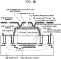
- Figs. 15 , 16 , and 17 are explanatory diagrams each schematically illustrating a pixel structure of the two-dimensional bolometer-type THz-wave detector described in PTL 4.
- NPL 1 Oda et. al., Proceedings of SPIE, Vol. 6940, 2008, pp. 69402Y-1 to 69402Y-12
- a THz-wave detector is preferably able to detect THz waves with higher-sensitivity.
- the THz-wave detector described in PTL 3 detects THz waves with high sensitivity by using an interference between a reflective film 103 and an absorption film 111 as illustrated in Fig. 14 .
- THz sensor sensitivity (hereinafter, simply referred to as "sensor sensitivity”) changes according to an angle between the polarization direction and the detector (polarization angle) is recognized when linear-polarized THz waves are incident on the detector.
- sensor sensitivity the dependence of the sensor sensitivity on the polarization angle is recognized.
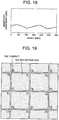
- Fig. 18 is a graph illustrating the dependence of the sensor sensitivity of the THz-wave detector as illustrated in Fig. 14 on the polarization angle.
- Fig. 19 is a top view of a reflective film 103 of arrayed pixels (the THz-wave detector illustrated in Fig. 14 ).
- Fig. 19 illustrates the top view looking down on the reflective film 103 for a plurality of arrayed pixels.
- a gap is formed between pixels in the reflective film 103.
- THz waves pass through the gap between the pixels in the reflective film 103 and a substrate 102 (specifically, the metal wiring of the reading circuit 102a of the substrate 102) reflects or absorbs the THz waves.
- the metal wiring of the reading circuit 102a normally includes a plurality of layers.
- Fig. 20 illustrates the THz reflection characteristics of the THz-wave detector in which the structure on the upper side than the reflective film 103 is not formed.
- Fig. 20 is a graph illustrating the dependence of a reflectance on a polarization angle in the case where the structure on the upper side than the reflective film 103 of the THz-wave detector illustrated in Fig. 14 is not formed.
- the THz reflectance drastically changes according to the polarization angle. If the shape of the gap in the reflective film 103 is reflected on the THz reflection characteristics, the THz reflection characteristics in that case are supposed to show a four-fold symmetry in which a symmetry is repeated every 90 degrees. It, however, can be estimated that reflection/absorption occurs from the metal wiring of the reading circuit 102a which is located in a lower part than the reflective film 103 since the THz reflection characteristics illustrated in Fig. 20 show a two-fold symmetry. Specifically, reflection/absorption in the metal wiring of the reading circuit 102a can be estimated from the graph illustrated in Fig. 20 .
- a terahertz-wave detector having a thermal separation structure in which a temperature detection unit including a bolometer thin film connected to electrode wiring is supported so as to be lifted above a substrate by a support part including the electrode wiring connected to a reading circuit formed on the substrate, wherein the terahertz-wave detector is provided with a reflective film that is formed on the substrate and reflects terahertz waves and an absorption film that is formed on the temperature detection unit and absorbs terahertz waves and the reflective film is integrally formed with the reflective film of an adjacent terahertz-wave detector.
- a terahertz-wave detector having a thermal separation structure in which a temperature detection unit including a bolometer thin film connected to electrode wiring is supported so as to be lifted above a substrate by a support part including the electrode wiring connected to a reading circuit formed on the substrate, wherein the terahertz-wave detector is provided with a second reflective film formed so as to cover a reflective film on the upper side of the reflective film that is formed on the substrate and reflects terahertz waves and an absorption film that is formed on the temperature detection unit and absorbs terahertz waves and the second reflective film is integrally formed with the second reflective film of an adjacent terahertz-wave detector.
- a terahertz-wave detector having a thermal separation structure in which a temperature detection unit including a bolometer thin film connected to electrode wiring is supported so as to be lifted above a substrate by a support part including the electrode wiring connected to a reading circuit formed on the substrate, wherein the terahertz-wave detector is provided with a reflective film that is formed on the substrate and reflects terahertz waves and an absorption film that is formed on the temperature detection unit and absorbs terahertz waves and the reflective film is formed without any space from the reflective film of an adjacent terahertz-wave detector.
- a terahertz-wave detector having a thermal separation structure in which a temperature detection unit including a bolometer thin film connected to electrode wiring is supported so as to be lifted above a substrate by a support part including the electrode wiring connected to a reading circuit formed on the substrate, wherein the terahertz-wave detector is provided with a reflective film that is formed on the substrate and reflects terahertz waves and an absorption film that is formed on the temperature detection unit and absorbs terahertz waves and the reflective film is formed so that the dependence on the polarization angle is smaller than a predetermined value.
- the present invention is able to reduce the dependence of the sensor sensitivity of the bolometer-type THz-wave detector on the polarization angle and to achieve higher-sensitivity THz wave detection.
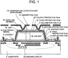
- Fig. 1 is an explanatory diagram schematically illustrating a pixel structure according to a first exemplary embodiment of a THz-wave detector according to the present invention.
- a sectional view of the THz-wave detector is illustrated.
- the THz-wave detector includes a reading circuit 2a, a substrate 2, a reflective film 3, a contact 4, a first protective film 5, electrode wiring 9, an eave-like member 12, a support part 13, and a temperature detection unit (diaphragm) 14.
- the substrate 2, the reading circuit 2a, the reflective film 3, the contact 4, the first protective film 5, the electrode wiring 9, the eave-like member 12, the support part 13, and the temperature detection unit 14 are the same as a substrate 102, a reading circuit 102a, a reflective film 103, a contact 104, a first protective film 105, electrode wiring 109, an eave-like member 112, a support part 113, and a temperature detection unit 114, and therefore the description thereof is omitted here.
- a second protective film 6, a third protective film 8, and a fourth protective film 10 included by the support part 13 are the same as a second protective film 106, a third protective film 108, and a fourth protective film 110 included by the support part 113 illustrated in Fig. 14 , and therefore the description thereof is omitted here.
- a bolometer thin film 7 and an absorption film 11 included by the temperature detection unit 14 are the same as a bolometer thin film 107 and an absorption film 111 included by the temperature detection unit 114 illustrated in Fig. 14 , and therefore the description thereof is omitted here.
- the reflective film 3 is formed so as to be integrated with an adjacent reflective film to prevent a gap from being formed between pixels adjacent to each other in the reflective film 3.
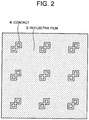
- Fig. 2 is a top view of the reflective film 3 illustrated in Fig. 1 .
- Fig. 2 illustrates a top view looking down on the reflective film 3 for a plurality of arrayed pixels.
- the reflective film 3 is arranged without a gap to prevent THz waves from passing through the gap so as to inhibit an occurrence of reflection or absorption from or into the metal wiring of the reading circuit 2a in this exemplary embodiment. This enables a reduction in the dependence of the THz reflectance of the substrate 2 on the polarization angle.
- the reflective film is integrally formed in this exemplary embodiment, the reflective film does not always need to be integrally formed, but the reflective film 3 may be formed separately as long as the gap is not formed.
- THz reflection characteristics of the THz-wave detector according to the present invention are described.
- the reflective film 3 is formed as illustrated in Fig. 1 and Figs. 3 and 4 illustrate the THz reflection characteristics of the THz-wave detector in which the structure on the upper side than the reflective film 3 is not formed.
- Fig. 3 is a graph illustrating the dependence of a reflectance of the THz-wave detector illustrated in Fig. 1 on a polarization angle in the case where the structure on the upper side than the reflective film 3 is not formed.
- Fig. 5 illustrates the dependence of the sensor sensitivity of the THz-wave detector of this exemplary embodiment on the polarization angle.
- any dependence of the sensor sensitivity on the polarization angle as in Fig. 18 is not found, and thus an advantageous effect of the present invention is obvious.
- Fig. 4 is a graph illustrating the dependence of a reflectance of the THz-wave detector illustrated in Fig. 1 on a frequency in the case where the structure on the upper side than the reflective film 3 is not formed.
- Fig. 4 illustrates the dependence of the THz reflectance on the frequency at the polarization angles of 0, 120, and 240 degrees.
- Fig. 21 is a graph illustrating the dependence of the reflectance of the THz-wave detector illustrated in Fig. 14 on the frequency in the case where the structure on the upper side than the reflective film 3 is not formed. In the graph illustrated in Fig. 4 , any large fluctuation of the THz reflectance caused by the frequency and the polarization angle as illustrated in Fig. 21 is not found.
- the THz-wave detector of this exemplary embodiment is able to reduce the variation of the dependence of the THz reflectance on the polarization angle caused by frequency and is able to maintain the dependence of the sensor sensitivity on the polarization angle to be low even if the frequency changes.
- the reflective film 3 is formed to prevent a gap from being formed between pixels in the reflective film 3 in the exemplary embodiment. This prevents THz waves from passing through the gap in the reflective film 3, thereby enabling a reduction in the dependence of the THz reflectance of the substrate 2 on the polarization angle. This makes it more difficult for such a phenomenon that an output (sensor sensitivity) from the THz-wave detector changes according to the polarization angle to occur.
- the present invention is able to reduce the dependence of the sensor sensitivity on the polarization angle in the THz-wave detector for detecting THz waves by using an interference between the reflective film and the absorption film as illustrated in Fig. 14 .
- the reflective film 3 may be arranged between the contact 4 and a contact of another pixel.
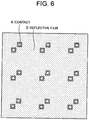
- the reflective film 3 is formed as illustrated in Fig. 6.
- Fig. 6 is a top view of the entire reflective film 3 in the case where the reflective film 3 is arranged between the contact 4 and a contact of another pixel.
- Fig. 6 illustrates the top view looking down on the reflective film 3 for a plurality of arrayed pixels. The formation of the reflective film 3 as in Fig. 6 enables the area of the reflective film 3 to increase as far as possible, thereby enabling a further reduction in the dependence of the sensor sensitivity of the THz-wave detector on the polarization angle.
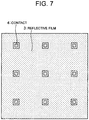
- one of the contacts 4 of the THz-wave detector may be electrically connected to a contact 4 of another THz-wave detector.
- the gap between the reflective film 3 and the contact 4 (a hole for the contact 4 formed in the reflective film 3), which is provided in the reflective film 3, can be reduced.
- the area of the reflective film 3 is able to be increased as far as possible, thereby enabling the dependence of the sensor sensitivity of the THz-wave detector on the polarization angle to be further reduced.
- Fig. 7 is a top view of the reflective film 3 in the case where the contact 4 is electrically connected to a contact of another pixel.
- Fig. 7 illustrates a top view looking down on the reflective film 3 for a plurality of arrayed pixels.
- Fig. 8 is an explanatory diagram schematically illustrating a pixel structure of the second exemplary embodiment of the THz-wave detector according to the present invention.
- Fig. 8 illustrates a sectional view of the THz-wave detector.
- the pixel structure of the second exemplary embodiment is the same as the pixel structure of the first exemplary embodiment. As illustrated in Fig. 8 , however, the THz-wave detector in this exemplary embodiment includes a second reflective film 3a in addition to the constituent elements illustrated in Fig. 1 .
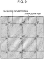
- Fig. 9 is a top view of the second reflective film 3a illustrated in Fig. 8 .
- Fig. 9 illustrates a top view looking down on the second reflective film 3a for a plurality of arrayed pixels.
- the second reflective film 3a is formed so as to cover the reflective film 3 as illustrated in Figs. 8 and 9 .
- the reflective film 3 and the second reflective film 3a are physically separated from each other.
- the second reflective film 3a and the absorption film 11 form an optical resonance structure.
- This exemplary embodiment is effective in the case where the reflective film 3 cannot be connected to a reflective film of an adjacent pixel according to convenience for manufacturing the THz sensor.
- a voltage is applied to the reflective film 3
- short-circuiting is likely to occur when the reflective film 3 is connected to a reflective film of an adjacent pixel.
- the second reflective film 3a physically separated from the reflective film 3 is formed so as to cover the reflective film 3, thereby achieving an equivalent advantageous effect to the first exemplary embodiment.
- the advantageous effect of the present invention is more obvious if the sheet resistance of the second reflective film 3a is 100 ⁇ /sq or less.
- Fig. 10 is an explanatory diagram schematically illustrating a pixel structure of the third exemplary embodiment of the THz-wave detector according to the present invention.
- Fig. 10 illustrates a sectional view of the THz-wave detector.
- the pixel structure of the third exemplary embodiment is the same as the pixel structure of the first exemplary embodiment.
- the THz-wave detector does not include the eave-like member 12.
- the film thickness of the first protective film 5 is set so that a gap (air gap 16) between the upper surface of the first protective film 5 and the lower surface of the temperature detection unit 14 is less than 8 ⁇ m without a change in the gap (gap 15) between the reflective film 3 and the absorption film 11.
- this exemplary embodiment is obtained by applying the reflective film 3 of the first exemplary embodiment to the THz-wave detector illustrated in Fig. 15 .
- the present invention may be applied to the THz-wave detector illustrated in Fig. 15 .
- an equivalent advantageous effect to the first exemplary embodiment is achieved also in the THz-wave detector as illustrated in Fig. 15 .
- the second reflective film 3a of the second exemplary embodiment may be applied to the THz-wave detector illustrated in Fig. 15 .
- an equivalent advantageous effect to the first exemplary embodiment is achieved even if the reflective film 3 cannot be connected to a reflective film of an adjacent pixel according to convenience for manufacturing the THz sensor.
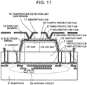
- Fig. 11 is an explanatory diagram schematically illustrating a pixel structure of the fourth exemplary embodiment of the THz-wave detector according to the present invention.
- Fig. 11 illustrates a sectional view of the THz-wave detector.
- the pixel structure of the fourth exemplary embodiment is the same as the pixel structure of the third exemplary embodiment. In this exemplary embodiment, however, the eave-like member 12 is formed over the temperature detection unit 14.
- this exemplary embodiment is obtained by applying the reflective film 3 of the first exemplary embodiment to the THz-wave detector illustrated in Fig. 16 .
- the present invention may be applied to the THz-wave detector illustrated in Fig. 16 .
- an equivalent advantageous effect to the first exemplary embodiment is achieved also in the THz-wave detector as illustrated in Fig. 16 .
- the second reflective film 3a of the second exemplary embodiment may be applied to the THz-wave detector illustrated in Fig. 16 .
- an equivalent advantageous effect to the first exemplary embodiment is achieved even if the reflective film 3 cannot be connected to a reflective film of an adjacent pixel according to convenience for manufacturing the THz sensor.
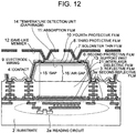
- Fig. 12 is an explanatory diagram schematically illustrating a pixel structure of the fifth exemplary embodiment of the THz-wave detector according to the present invention.
- Fig. 12 illustrates a sectional view of the THz-wave detector.
- the pixel structure of the fifth exemplary embodiment is the same as the pixel structure of the second exemplary embodiment.
- a multilayer wiring structure for connecting the electrode wiring 9 to the reading circuit 2a is formed by sequentially laminating a via and a wiring layer on the wiring used as the reflective film 3 by using a wiring forming method in a semiconductor manufacturing process. Thereby, breakage of the electrode wiring 9 can be suppressed.
- the interlayer dielectric film 21 is a dielectric film between laminated wiring layers.
- this exemplary embodiment is obtained by applying the second reflective film 3a of the second exemplary embodiment to the THz-wave detector illustrated in Fig. 17 .
- the present invention may be applied to the THz-wave detector illustrated in Fig. 17 .
- an equivalent advantageous effect to the first exemplary embodiment is achieved even if the reflective film 3 is not able to be connected to the reflective film of an adjacent pixel according to convenience for manufacturing the THz sensor in the THz-wave detector as illustrated in Fig. 17 .
- the reflective film 3 of the first exemplary embodiment may be applied to the THz-wave detector illustrated in Fig. 17 .
- the THz-wave detector illustrated in Fig. 17 may include the reflective film 3 instead of the reflective film 103.
- an equivalent advantageous effect to the first exemplary embodiment is achieved.
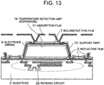
- Fig. 13 is an explanatory diagram illustrating the minimum configuration of the terahertz-wave detector according to the present invention.
- the terahertz-wave detector according to the present invention is a terahertz-wave detector having a thermal separation structure in which a temperature detection unit 14 including a bolometer thin film 7 connected to electrode wiring 9 is supported so as to be lifted above a substrate 2 by a support part 13 including the electrode wiring 9 connected to a reading circuit 2a formed on the substrate 2, wherein the terahertz-wave detector is provided with a reflective film 3 that is formed on the substrate 2 and reflects terahertz waves and an absorption film 11 that is formed on the temperature detection unit 14 and absorbs terahertz waves and the reflective film 3 is integrally formed with the reflective film of an adjacent terahertz-wave detector.
- the present invention is able to prevent THz waves from passing through a gap in the reflective film 3 and to reduce the dependence of the THz reflectance of the substrate 2 on the polarization angle. This makes it more difficult for such a phenomenon that an output (sensor sensitivity) from the detector changes according to the polarization angle to occur.
- the present invention is able to reduce the dependence of the sensor sensitivity on the polarization angle in the THz-wave detector for detecting THz waves by using an interference between the reflective film and the absorption film as illustrated in Fig. 14 .
- the sheet resistance of the reflective film 3 may be 100 ⁇ /sq or less. This configuration enables the dependence of the sensor sensitivity of the THz-wave detector on the polarization angle to be further reduced.
- a hole for a contact 4 may be formed in the reflective film 3 according to the area of the contact 4 electrically connecting the reading circuit 2a formed on the substrate 2 to the electrode wiring 9 included by the support part 13.
- the terahertz-wave detector according to the present invention is a terahertz-wave detector having a thermal separation structure in which a temperature detection unit 14 including a bolometer thin film 7 connected to electrode wiring 9 is supported so as to be lifted above a substrate 2 by a support part 13 including the electrode wiring 9 connected to a reading circuit 2a formed on the substrate 2, wherein the terahertz-wave detector is provided with a second reflective film 3a formed so as to cover a reflective film 3 on the upper side of the reflective film 3 that is formed on the substrate 2 and reflects terahertz waves and an absorption film 11 that is formed on the temperature detection unit 14 and absorbs terahertz waves and the second reflective film 3a is integrally formed with the second reflective film of an adjacent terahertz-wave detector.
- the second reflective film 3a that covers the reflective film 3 is integrally formed with the second reflective film of the adjacent pixel instead of integrally forming the reflective film 3 with the reflective film of the adjacent pixel in this manner, the dependence of the sensor sensitivity of the THz-wave detector on the polarization angle can be reduced even in the case where the reflective film 3 cannot be connected to the reflective film of the adjacent pixel according to convenience for manufacturing the THz sensor.
- the reflective film 3 and the second reflective film 3a may be separated from each other.
- the reflective film 3 and the second reflective film 3a are physically separated from each other, thereby enabling a reduction in the dependence of the sensor sensitivity of the THz-wave detector on the polarization angle.
- the sheet resistance of the second reflective film 3a may be 100 ⁇ /sq or less. This configuration enables the dependence of the sensor sensitivity of the THz-wave detector on the polarization angle to be further reduced.
- the terahertz-wave detector according to the present invention is a terahertz-wave detector having a thermal separation structure in which a temperature detection unit 14 including a bolometer thin film 7 connected to electrode wiring 9 is supported so as to be lifted above a substrate 2 by a support part 13 including the electrode wiring 9 connected to a reading circuit 2a formed on the substrate 2, wherein the terahertz-wave detector is provided with a reflective film 3 that is formed on the substrate 2 and reflects terahertz waves and an absorption film 11 that is formed on the temperature detection unit 14 and absorbs terahertz waves and the reflective film 3 is formed without any space from the reflective film of an adjacent terahertz-wave detector.
- THz waves can be prevented from passing through the gap in the reflective film 3 even in the case where the reflective film is separated from the reflective film of the adjacent terahertz-wave detector and not integrally formed with the reflective film thereof. This enables a reduction in the dependence of the THz reflectance of the substrate 2 on the polarization angle.
- the terahertz-wave detector according to the present invention is a terahertz-wave detector having a thermal separation structure in which a temperature detection unit 14 including a bolometer thin film 7 connected to electrode wiring 9 is supported so as to be lifted above a substrate 2 by a support part 13 including the electrode wiring 9 connected to a reading circuit 2a formed on the substrate 2, wherein the terahertz-wave detector is provided with a reflective film 3 that is formed on the substrate 2 and reflects terahertz waves and an absorption film 11 that is formed on the temperature detection unit 14 and absorbs terahertz waves and the reflective film 3 is formed so that the dependence of the terahertz-wave reflectance on the polarization angle is smaller than a predetermined value.
- This configuration makes it more difficult for such a phenomenon that an output (sensor sensitivity) from the THz-wave detector changes according to the polarization angle to occur.
Landscapes
- Physics & Mathematics (AREA)
- General Physics & Mathematics (AREA)
- Spectroscopy & Molecular Physics (AREA)
- Engineering & Computer Science (AREA)
- Manufacturing & Machinery (AREA)
- Photometry And Measurement Of Optical Pulse Characteristics (AREA)
Applications Claiming Priority (2)
| Application Number | Priority Date | Filing Date | Title |
|---|---|---|---|
| JP2014086412 | 2014-04-18 | ||
| PCT/JP2015/002076 WO2015159540A1 (ja) | 2014-04-18 | 2015-04-15 | テラヘルツ波検出器 |
Publications (2)
| Publication Number | Publication Date |
|---|---|
| EP3133379A1 true EP3133379A1 (de) | 2017-02-22 |
| EP3133379A4 EP3133379A4 (de) | 2017-11-22 |
Family
ID=54323763
Family Applications (1)
| Application Number | Title | Priority Date | Filing Date |
|---|---|---|---|
| EP15780439.4A Withdrawn EP3133379A4 (de) | 2014-04-18 | 2015-04-15 | Terahertzwellendetektor |
Country Status (5)
| Country | Link |
|---|---|
| US (1) | US20170030775A1 (de) |
| EP (1) | EP3133379A4 (de) |
| JP (1) | JP6292297B2 (de) |
| CA (1) | CA2945597C (de) |
| WO (1) | WO2015159540A1 (de) |
Families Citing this family (3)
| Publication number | Priority date | Publication date | Assignee | Title |
|---|---|---|---|---|
| JP2017101956A (ja) * | 2015-11-30 | 2017-06-08 | 国立大学法人 東京大学 | ボロメータ型テラヘルツ波検出素子アレイ |
| JP6814442B2 (ja) * | 2015-11-30 | 2021-01-20 | 国立大学法人 東京大学 | ボロメータ型テラヘルツ波検出素子およびボロメータ型テラヘルツ波検出素子アレイ |
| CN107128872B (zh) * | 2017-05-11 | 2018-09-18 | 烟台睿创微纳技术股份有限公司 | 一种新型偏振非制冷红外焦平面探测器及其制备方法 |
Family Cites Families (12)
| Publication number | Priority date | Publication date | Assignee | Title |
|---|---|---|---|---|
| JP3921320B2 (ja) * | 2000-01-31 | 2007-05-30 | 日本電気株式会社 | 熱型赤外線検出器およびその製造方法 |
| JP3409848B2 (ja) * | 2000-08-29 | 2003-05-26 | 日本電気株式会社 | 熱型赤外線検出器 |
| FR2855609B1 (fr) * | 2003-05-26 | 2005-07-01 | Commissariat Energie Atomique | Dispositif de detection bolometrique a antenne, a cavite optimisee, pour ondes electromagnetiques millimetriques ou submillimetriques, et procede de fabrication de ce dispositif |
| JP2005043381A (ja) * | 2004-10-18 | 2005-02-17 | Nec Corp | 熱型赤外線検出器およびその製造方法 |
| FR2919049B1 (fr) * | 2007-07-20 | 2009-10-02 | Ulis Soc Par Actions Simplifie | Detecteur de rayonnement electromagnetique et procede de fabrication d'un tel detecteur |
| JP2009222649A (ja) * | 2008-03-18 | 2009-10-01 | Mitsubishi Electric Corp | 赤外線撮像素子およびその製造方法 |
| US8495882B2 (en) * | 2009-08-10 | 2013-07-30 | General Electric Company | Syngas cleanup section with carbon capture and hydrogen-selective membrane |
| JP5964543B2 (ja) * | 2010-06-15 | 2016-08-03 | 日本電気株式会社 | ボロメータ型テラヘルツ波検出器 |
| EP2618817B1 (de) * | 2010-07-31 | 2018-06-13 | The Scripps Research Institute | Auf liposome zielende verbindungen und verwendungen davon |
| FR2977937B1 (fr) * | 2011-07-15 | 2013-08-16 | Centre Nat Rech Scient | Detecteur bolometrique a performances ameliorees |
| JP2013164364A (ja) * | 2012-02-13 | 2013-08-22 | Seiko Epson Corp | テラヘルツカメラ及び電子機器 |
| JP5943764B2 (ja) * | 2012-08-02 | 2016-07-05 | 三菱電機株式会社 | 電磁波センサ及び電磁波センサ装置 |
-
2015
- 2015-04-04 US US15/302,237 patent/US20170030775A1/en not_active Abandoned
- 2015-04-15 CA CA2945597A patent/CA2945597C/en active Active
- 2015-04-15 JP JP2016513642A patent/JP6292297B2/ja active Active
- 2015-04-15 WO PCT/JP2015/002076 patent/WO2015159540A1/ja not_active Ceased
- 2015-04-15 EP EP15780439.4A patent/EP3133379A4/de not_active Withdrawn
Non-Patent Citations (1)
| Title |
|---|
| See references of WO2015159540A1 * |
Also Published As
| Publication number | Publication date |
|---|---|
| JP6292297B2 (ja) | 2018-03-14 |
| JPWO2015159540A1 (ja) | 2017-04-13 |
| CA2945597A1 (en) | 2015-10-22 |
| EP3133379A4 (de) | 2017-11-22 |
| CA2945597C (en) | 2019-01-15 |
| US20170030775A1 (en) | 2017-02-02 |
| WO2015159540A1 (ja) | 2015-10-22 |
Similar Documents
| Publication | Publication Date | Title |
|---|---|---|
| US8541742B2 (en) | Bolometer-type THz wave detector | |
| US9520510B2 (en) | Embedded optical sensors using transverse Fabry-Perot resonator as detectors | |
| US9638578B2 (en) | Terahertz wave detecting device, camera, imaging apparatus, and measuring apparatus | |
| US8598528B2 (en) | Infrared detector based on suspended bolometric micro-plates | |
| EP3106910A1 (de) | Fabry-perot-interferenzfilter | |
| EP2947432A1 (de) | Infrarotdetektionselement, infrarotdetektor und infrarot-gassensor | |
| KR20140104915A (ko) | 테라헤르츠파 검출 장치, 카메라, 이미징 장치 및 계측 장치 | |
| US11215510B2 (en) | Thermal infrared detector and manufacturing method for thermal infrared detector | |
| US20170229522A1 (en) | Organic light emitting display panel and method for manufacturing the same | |
| JP2013246021A5 (de) | ||
| EP3133379A1 (de) | Terahertzwellendetektor | |
| CN111213117A (zh) | 触控面板、触控面板制备方法及触控装置 | |
| US20160219650A1 (en) | Infrared radiation device and production method for same | |
| US11255730B2 (en) | Light detector | |
| CN107608017B (zh) | 法布里-珀罗干涉滤光片以及光检测装置 | |
| US10566489B2 (en) | Photosensor | |
| US12379255B2 (en) | Electromagnetic wave sensor | |
| US10852194B2 (en) | Light detector | |
| US20200249084A1 (en) | Light detector | |
| JP6834974B2 (ja) | ボロメータ型テラヘルツ波検出器 | |
| JP2015135264A (ja) | 焦電型光検出器、焦電型光検出装置、電子機器 | |
| JP2013160708A (ja) | 焦電型検出器、焦電型検出装置及び電子機器 | |
| JP2025093416A (ja) | 赤外線センサ、及び赤外線センサの製造方法 | |
| JP2016009778A (ja) | 光伝導アンテナ、テラヘルツ波発生装置、カメラ、イメージング装置、および計測装置 | |
| JP2014153187A (ja) | 半導体物理量センサ |
Legal Events
| Date | Code | Title | Description |
|---|---|---|---|
| PUAI | Public reference made under article 153(3) epc to a published international application that has entered the european phase |
Free format text: ORIGINAL CODE: 0009012 |
|
| 17P | Request for examination filed |
Effective date: 20161117 |
|
| AK | Designated contracting states |
Kind code of ref document: A1 Designated state(s): AL AT BE BG CH CY CZ DE DK EE ES FI FR GB GR HR HU IE IS IT LI LT LU LV MC MK MT NL NO PL PT RO RS SE SI SK SM TR |
|
| AX | Request for extension of the european patent |
Extension state: BA ME |
|
| DAV | Request for validation of the european patent (deleted) | ||
| DAX | Request for extension of the european patent (deleted) | ||
| A4 | Supplementary search report drawn up and despatched |
Effective date: 20171020 |
|
| RIC1 | Information provided on ipc code assigned before grant |
Ipc: G01J 5/20 20060101ALI20171016BHEP Ipc: G01J 1/02 20060101AFI20171016BHEP Ipc: G01J 5/08 20060101ALI20171016BHEP |
|
| 17Q | First examination report despatched |
Effective date: 20190910 |
|
| STAA | Information on the status of an ep patent application or granted ep patent |
Free format text: STATUS: THE APPLICATION HAS BEEN WITHDRAWN |
|
| 18W | Application withdrawn |
Effective date: 20191029 |