EP3135780A1 - Procédé de fabrication d'alliage de cuivre et alliage de cuivre - Google Patents
Procédé de fabrication d'alliage de cuivre et alliage de cuivre Download PDFInfo
- Publication number
- EP3135780A1 EP3135780A1 EP16794497.4A EP16794497A EP3135780A1 EP 3135780 A1 EP3135780 A1 EP 3135780A1 EP 16794497 A EP16794497 A EP 16794497A EP 3135780 A1 EP3135780 A1 EP 3135780A1
- Authority
- EP
- European Patent Office
- Prior art keywords
- powder
- phase
- copper alloy
- copper
- manufacturing
- Prior art date
- Legal status (The legal status is an assumption and is not a legal conclusion. Google has not performed a legal analysis and makes no representation as to the accuracy of the status listed.)
- Granted
Links
Images












Classifications
-
- C—CHEMISTRY; METALLURGY
- C22—METALLURGY; FERROUS OR NON-FERROUS ALLOYS; TREATMENT OF ALLOYS OR NON-FERROUS METALS
- C22C—ALLOYS
- C22C9/00—Alloys based on copper
-
- B—PERFORMING OPERATIONS; TRANSPORTING
- B22—CASTING; POWDER METALLURGY
- B22F—WORKING METALLIC POWDER; MANUFACTURE OF ARTICLES FROM METALLIC POWDER; MAKING METALLIC POWDER; APPARATUS OR DEVICES SPECIALLY ADAPTED FOR METALLIC POWDER
- B22F3/00—Manufacture of workpieces or articles from metallic powder characterised by the manner of compacting or sintering; Apparatus specially adapted therefor ; Presses and furnaces
- B22F3/10—Sintering only
- B22F3/105—Sintering only by using electric current other than for infrared radiant energy, laser radiation or plasma ; by ultrasonic bonding
-
- C—CHEMISTRY; METALLURGY
- C22—METALLURGY; FERROUS OR NON-FERROUS ALLOYS; TREATMENT OF ALLOYS OR NON-FERROUS METALS
- C22C—ALLOYS
- C22C1/00—Making non-ferrous alloys
- C22C1/04—Making non-ferrous alloys by powder metallurgy
- C22C1/0425—Copper-based alloys
-
- B—PERFORMING OPERATIONS; TRANSPORTING
- B22—CASTING; POWDER METALLURGY
- B22F—WORKING METALLIC POWDER; MANUFACTURE OF ARTICLES FROM METALLIC POWDER; MAKING METALLIC POWDER; APPARATUS OR DEVICES SPECIALLY ADAPTED FOR METALLIC POWDER
- B22F3/00—Manufacture of workpieces or articles from metallic powder characterised by the manner of compacting or sintering; Apparatus specially adapted therefor ; Presses and furnaces
- B22F3/10—Sintering only
- B22F3/105—Sintering only by using electric current other than for infrared radiant energy, laser radiation or plasma ; by ultrasonic bonding
- B22F2003/1051—Sintering only by using electric current other than for infrared radiant energy, laser radiation or plasma ; by ultrasonic bonding by electric discharge
-
- B—PERFORMING OPERATIONS; TRANSPORTING
- B22—CASTING; POWDER METALLURGY
- B22F—WORKING METALLIC POWDER; MANUFACTURE OF ARTICLES FROM METALLIC POWDER; MAKING METALLIC POWDER; APPARATUS OR DEVICES SPECIALLY ADAPTED FOR METALLIC POWDER
- B22F2998/00—Supplementary information concerning processes or compositions relating to powder metallurgy
- B22F2998/10—Processes characterised by the sequence of their steps
Definitions
- the present invention relates to a method for manufacturing a copper alloy and to a copper alloy.
- One previously proposed copper alloy manufacturing method includes a sintering step of subjecting a binary Cu-Zr alloy powder having an average particle diameter of 30 ⁇ m or less and having a hypoeutectic composition containing Zr in an amount of from 5.00 at% to 8.00 at% to spark plasma sintering at a temperature of 0.9 Tm°C or lower (Tm°C is the melting point of the alloy powder) by supplying DC pulse current (see, for example, PTL 1).
- Tm°C is the melting point of the alloy powder
- the binary Cu-Zr alloy powder produced from a binary Cu-Zr alloy having a hypoeutectic composition by a high-pressure gas atomization method is subjected to spark plasma sintering (SPS).
- SPS spark plasma sintering
- the present invention has been made in view of the above problem, and a principal object is to provide a copper alloy manufacturing method that allows a copper alloy having increased electrical conductivity and mechanical strength to be produced using a simpler process and to provide this copper alloy.
- the present inventors have conducted extensive studies in order to achieve the above principal object and found that a copper alloy having increased electrical conductivity and mechanical strength can be produced by a simpler process when a copper powder and a Cu-Zr master alloy or the copper powder and a ZrH 2 powder are used as raw material powders and subjected to spark plasma sintering. Thus, the present invention has been completed.
- a method for manufacturing a copper alloy according to the present invention comprises
- a copper alloy according to the present invention has a structure in which a second phase is dispersed in a ⁇ -Cu matrix phase and has the following features (1) to (3):
- the present invention allows a copper alloy having increased electrical conductivity and mechanical strength to be produced by a simpler process.
- the reason for this may be as follows.
- metal powders can be highly reactive, but this depends on the elements of the powders.
- Zr powder is highly reactive with oxygen and must be handled with extreme care when it is used as a raw material powder in air.
- a Cu-Zr master alloy powder e.g., a Cu-50 mass% Zr master alloy
- a ZrH 2 powder are relatively stable and are easy to handle even in air. Therefore, the above copper alloy can be produced using a relatively simple process including mixing and pulverizing raw materials including such a powder and then subjecting the mixture to spark plasma sintering.
- the method for manufacturing a copper alloy according to the present invention includes (a) a pulverization step of obtaining a raw material powder mixture and (b) a sintering step of subjecting the powder mixture to spark plasma sintering (SPS).
- SPS spark plasma sintering
- a copper powder and a Cu-Zr master alloy are weighed, or the copper powder and a ZrH 2 powder are weighed. Specifically, these are weighed such that an alloy composition of Cu-xZr (x is the atomic% (hereinafter abbreviated as at%) of Zr, and 0.5 ⁇ x ⁇ 8.6 is satisfied) is obtained and are then pulverized and mixed in an inert atmosphere until the average particle diameter D50 falls within the range of from 1 ⁇ m to 500 ⁇ m to thereby obtain a powder mixture.
- x is the atomic% (hereinafter abbreviated as at%) of Zr, and 0.5 ⁇ x ⁇ 8.6 is satisfied) is obtained and are then pulverized and mixed in an inert atmosphere until the average particle diameter D50 falls within the range of from 1 ⁇ m to 500 ⁇ m to thereby obtain a powder mixture.
- the raw materials (the copper powder and the Cu-Zr master alloy, or the copper powder and the ZrH 2 powder) may be weighed such that an alloy composition of Cu-xZr (0.5 at% ⁇ x ⁇ 8.6 at%) is obtained.
- the copper powder has an average particle diameter of, for example, preferably 180 ⁇ m or less, more preferably 75 ⁇ m or less, and still more preferably 5 ⁇ m or less.
- the copper powder has an average particle diameter of, for example, preferably 100 ⁇ m or less, more preferably 50 ⁇ m or less, and still more preferably 25 ⁇ m or less.
- the above average particle diameter is a D50 particle diameter measured using a laser diffraction particle size distribution measurement device.
- the copper powder is composed of copper and inevitable components. More preferably, the copper powder is oxygen-free copper (JIS C1020).
- the inevitable components include Be, Mg, Al, Si, P, Ti, Cr, Mn, Fe, Co, Ni, Zn, Sn, Pb, Nb, and Hf.
- the content of the inevitable components with respect to the total mass may be 0.01% by mass or less.
- the Cu-Zr master alloy may be in the form of ingot or metal pieces but is preferably in the form of fine metal particles because it can be easily pulverized and mixed.
- the Cu-Zr alloy has an average particle diameter of, for example, preferably 250 ⁇ m or less and more preferably 20 ⁇ m or less.
- This ZrH 2 powder is preferable because it is relatively chemically stable and can provide good workability in air.
- the ZrH 2 powder has an average particle diameter of, for example, 10 ⁇ m or less and more preferably 5 ⁇ m or less.
- the above components are mixed at an alloy composition of Cu-xZr (0.5 at% ⁇ x ⁇ 8.6 at%), but x may fall within the range of, for example, 5.0 at% ⁇ x ⁇ 8.6 at%.
- the alloy composition may be such that x falls within the range of 0.5 at% ⁇ x ⁇ 5.0 at%.
- the above components are mixed at an alloy composition of Cu 1-x Zr x (0.005 ⁇ X ⁇ 0.086), but X may fall within the range of, for example, 0.05 ⁇ X ⁇ 0.086.
- the alloy composition may be such that X falls within the range of 0.005 ⁇ X ⁇ 0.05.
- the electrical conductivity tends to increase.
- the copper powder, the Cu-Zr master alloy or the ZrH 2 powder, and a grinding medium may be sealed in a closed container and then mixed and pulverized. In this step, it is preferable to mix and pulverize the components using, for example, a ball mill.
- the grinding medium may be agate (SiO 2 ), alumina (Al 2 O 3 ), silicon nitride (SiC), zirconia (ZrO 2 ), stainless steel (Fe-Cr-Ni), chromium steel (Fe-Cr), cemented carbide (WC-Co), etc.
- the grinding medium is Zr balls.
- the atmosphere inside the closed container is an inert atmosphere such as a nitrogen, He, or Ar atmosphere.
- the process time for the mixing and pulverization may be determined empirically such that the average particle diameter D50 falls within the range of 1 ⁇ m to 500 ⁇ m.
- the process time may be, for example, 12 hours or longer and may be 24 hours or longer.
- the powder mixture has an average particle diameter D50 of 100 ⁇ m or less, more preferably 50 ⁇ m or less, and still more preferably 20 ⁇ m or less. The smaller the particle diameter of the powder mixture subjected to mixing and pulverization, the more preferable. This is because the copper alloy obtained can be more uniform.
- the powder mixture obtained by pulverization and mixing may contain, for example, the Cu powder and a Zr powder or may contain a Cu-Zr alloy powder.
- the powder mixture obtained by pulverization and mixing may be, for example, at least partially alloyed in the course of pulverization and mixing.
- the powder mixture is subjected to spark plasma sintering by holding the powder mixture at a prescribed temperature lower than eutectic temperature while the powder mixture is pressurized at a pressure within a prescribed range.
- the powder mixture may be inserted into a graphite-made die and subjected to spark plasma sintering in a vacuum.
- the vacuum condition may be, for example, 200 Pa or less, 100 Pa or less, or 1 Pa or less.
- the spark plasma sintering may be performed at a temperature lower by 400°C to 5°C than the eutectic temperature (e.g., 600°C to 950°C) or at a temperature lower by 272°C to 12°C than the eutectic temperature.
- the spark plasma sintering may be performed at a temperature of 0.9 Tm°C or lower (Tm (°C) is the melting point of the alloy powder).
- Tm (°C) is the melting point of the alloy powder.
- the condition for pressurizing the powder mixture may be within the range of from 10 MPa to 100 MPa or within the range of 60 MPa or less. In this manner, a dense copper alloy can be obtained.
- the holding time under pressure is preferably 5 minutes or longer, more preferably 10 minutes or longer, and still more preferably 15 minutes or longer.
- the holding time under pressure is preferably within the range of 100 minutes or shorter.
- a direct current within the range of from 500 A to 2,000 A is supplied between the die and a base plate.
- the copper alloy according to the present invention has a structure in which a second phase is dispersed in a Cu matrix phase and has the following features (1) to (3).
- the copper alloy may further have at least one of features (4) and (5).
- the Cu matrix phase is a phase containing Cu and may be, for example, a phase containing ⁇ -Cu.
- the Cu phase can increase electrical conductivity and can also increase processability.
- the Cu phase contains no eutectic phase.
- the eutectic phase is a phase containing, for example, Cu and a Cu-Zr-based compound.
- the average particle diameter D50 of the second phase is determined as follows. First, a backscattered electron image of a cross section of a specimen is observed at 100X to 500X using a scanning electron microscope (SEM). Then the diameters of inscribed circles of particles in the image are determined and used as the diameters of the particles. Specifically, the diameters of all the particles present in the field of view are determined. This procedure is repeated for a plurality of fields of view (e.g., five fields of view). The particle diameters obtained are used to determine a cumulative distribution, and its median diameter is used as the average particle diameter D50. In this copper alloy, it is preferable that the Cu-Zr-based compound phase contains Cu 5 Zr.
- the Cu-Zr-based compound phase may be a single phase or may be a phase containing two or more Cu-Zr-based compounds.
- the Cu-Zr-based compound phase may be a single phase such as a Cu 9 Zr 2 phase, a Cu 5 Zr phase, or a Cu 8 Zr 3 phase, may include the Cu 5 Zr phase as a main phase and another Cu-Zr-based compound (Cu 9 Zr 2 or Cu 8 Zr 3 ) as a subphase, or may include the Cu 9 Zr 2 phase as a main phase and another Cu-Zr-based compound (Cu 5 Zr or Cu 8 Zr 3 ) as a subphase.
- the main phase is a phase with the highest abundance (with the largest volume fraction or the largest area fraction in an observation region).
- the subphase in the Cu-Zr-based compound phase is a phase other than the main phase.
- the Cu-Zr-based compound phase has, for example, high Young's modulus and high hardness, so that the presence of the Cu-Zr-based compound phase allows the mechanical strength of the copper alloy to be increased.
- the Zr phase in the second phase may contain Zr in an amount of, for example, 90 at% or more, 92 at% or more, or 94 at% or more.
- an oxide film may be formed in its outermost shell. The presence of the oxide film may suppress diffusion of Cu into the second phase.
- many fine distorted particles may form twin crystals.
- the fine particles may be the Zr phase, and the Cu-Zr-based compound phase may be formed in the distorted portions.
- the copper alloy may be formed at a hypoeutectic composition by subjecting a copper powder and a Cu-Zr master alloy or the copper powder and a ZrH 2 powder to spark plasma sintering.
- the spark plasma sintering may be performed using the process described above.
- the hypoeutectic composition may be, for example, a composition containing from 0.5 at% to 8.6 at% of Zr with the balance being Cu.
- the copper alloy may contain inevitable components (e.g., a trace amount of oxygen).
- the content of oxygen is, for example, preferably 700 ppm or less and may be 200 ppm to 700 ppm.
- the inevitable components include Be, Mg, Al, Si, P, Ti, Cr, Mn, Fe, Co, Ni, Zn, Sn, Pb, Nb, and Hf.
- the content of the inevitable components with respect to the total mass may be within the range of 0.01% by mass or less.
- the copper alloy may have a composition obtained by diluting the composition shown in Table 1 until the content of Zr falls within the range of from 0.5 at% to 8.6 at%.
- the copper alloy of the present invention may have a tensile strength of 200 MPa or more.
- the copper alloy of the present invention may have an electrical conductivity of 20%IACS or more.
- the tensile strength is a value measured according to JIS-Z2201.
- the electrical conductivity is determined by measuring the volume resistivity of the copper alloy according to JIS-H0505 and computing the ratio of the resistance value of annealed pure copper (0.017241 ⁇ cm) to the measured volume resistivity to convert the volume resistivity to electrical conductivity (%IACS).
- the copper alloy in the present embodiment and the manufacturing method therefor have been described above in detail. With this manufacturing method, a copper alloy having increased electrical conductivity and mechanical strength can be produced using a simpler process.
- the reason for this may be as follows.
- metal powders can be high reactive with oxygen, but this depends on the elements of the powders.
- Zr powder is highly reactive and must be handled with extreme care when it is used as a raw material powder in air, in order to avoid danger such as an explosion.
- the Cu-Zr master alloy powder e.g., a Cu-50 mass% Zr master alloy
- the ZrH 2 powder are relatively stable and are easy to handle.
- the copper alloy having increased electrical conductivity and mechanical strength can be produced using a relatively simple process including mixing and pulverizing raw materials including such a powder and then subjecting the mixture to spark plasma sintering.
- this copper alloy is used for, for example, discharge electrodes or sliding components, these can have a low friction coefficient and are stable, and abrasion loss and weight loss can be reduced.
- Experimental Examples which are examples in which specific copper alloys were produced, will be described below.
- Experimental Examples 3-1 to 3-3 and 4-1 to 4-3 correspond to Examples of the present invention, and Experimental Examples 1-1 to 1-3 and 2-1 to 2-3 correspond to Reference Examples.
- Cu-Zr-based alloy powders produced by a high-pressure Ar gas atomization method for pulverization were used.
- the average particle diameters D50 of these alloy powders were 20 to 28 ⁇ m.
- the contents of Zr in the Cu-Zr-based alloy powders were 1 at%, 3 at%, and 5 at%, respectively, and the Cu-Zr-based alloy powders were used as alloy powders in Experimental Examples 1-1 to 1-3, respectively.
- the particle size of each of the alloy powders was measured using a laser diffraction particle size distribution measurement device (SALD-3000J) manufactured by Shimadzu Corporation.
- the content of oxygen in each powder was 0.100 mass%.
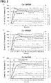
- the SPS (spark plasma sintering) used as the sintering step was performed using a spark plasma sintering apparatus (Model: SPS-210LX) manufactured by SPS Syntex, Inc. 40 g of one of the powders was placed in a graphite-made die having a cavity of a diameter of 20 mm x 10 mm, and a DC pulse current of 3 kA to 4 kA was supplied under the conditions of a temperature rise rate of 0.4 K/s, a sintering temperature of 1,173K (about 0.9 Tm, Tm: the melting point of the alloy), a holding time of 15 minutes, and a pressure of 30 MPa.
- Each of the copper alloys (SPS materials) in Experimental Examples 1-1 to 1-3 was produced in the manner described above. The copper alloys produced in this manner are collectively referred to as a "copper alloy in Experimental Example 1.”
- FIG. 1 shows the particle size distribution of the powder mixture in Experimental Example 3.
- Cu-Zr-based alloy powders were prepared such that the contents of Zr were 1 at%, 3 at%, and 5 at%, respectively, and were used as alloy powders in Experimental Examples 3-1 to 3-3. These powders were subjected to the same step as in Experimental Example 1, and each of the copper alloys obtained was used as a copper alloy in Experimental Example 3 (3-1 to 3-3).
- Fig. 2 shows illustrations of the SPS conditions in Experimental Example 3.
- the powder obtained was used to prepare Cu-Zr-based alloy powders such that the contents of Zr were 1 at%, 3 at%, and 5 at%, respectively, and were used as alloy powders in Experimental Examples 4-1 to 4-3. These powders were subjected to the same step as in Experimental Example 1, and each of the copper alloys obtained was used as a copper alloy in Experimental Example 4 (4-1 to 4-3).
- Microstructural observation was performed using a scanning electron microscope (SEM), a scanning transmission electron microscope (STEM), and a nano-beam electron diffraction (NBD) method.
- SEM observation was performed using S-5500 manufactured by Hitachi High-Technologies, and a secondary electron image and a backscattered electron image were taken at an acceleration voltage of 2.0 kV.
- the TEM observation was performed using JEM-2100F manufactured by JEOL Ltd. In this case, a BF-STEM image and a HAADF-STEM image were taken at an acceleration voltage of 200 kV, and nano-electron beam diffraction was performed.
- Elementary analysis by EDX JED-2300T manufactured by JEOL Ltd.
- a measurement specimen was prepared by ion-milling at an acceleration voltage of 5.5 kV using a cross section polisher (CP) SM-09010 manufactured by JEOL Ltd. with an argon ion source.
- Compound phases were identified by an X-ray diffraction method using Co-K ⁇ radiation.
- RINT RAPID II manufactured by Rigaku Corporation was used for the XRD measurement.
- the electric properties of the obtained SPS materials in the Experimental Examples and drawn wire materials were examined at room temperature by probe-type electrical conductivity measurement and four-terminal electrical resistance measurement at a length of 500 mm.
- the Young's modulus E and the hardness H by the nano-indentation method were measured.
- the measurement apparatus used was Nano Indenter XP/DCM manufactured by Agilent Technologies.
- the indenter head used was XP, and a diamond Berkovich indenter was used.
- Test Works 4 manufactured by Agilent Technologies was used as analysis software.
- measurement conditions were as follows: measurement mode: CSM (Continuous Stiffness Measurement), excitation vibration frequency: 45 Hz, excitation vibration amplitude: 2 nm, strain rate: 0.05 s -1 , indentation depth: 1,000 nm, the number of measurement points N: 5, measurement point interval: 5 ⁇ m, measurement temperature: 23°C, and standard sample: fused silica.
- CSM Continuous Stiffness Measurement
- excitation vibration frequency 45 Hz
- excitation vibration amplitude 2 nm
- strain rate 0.05 s -1
- indentation depth 1,000 nm
- the number of measurement points N 5
- measurement point interval 5 ⁇ m
- measurement temperature 23°C
- standard sample fused silica.
- a sample was subjected to cross-section processing using a cross section polisher (CP). The sample was then fixed to a sample stage using a hot-melt adhesive by heating them at 100°C for 30 seconds.
- the sample fixed to the sample stage was attached to the measurement apparatus to measure the Young's modulus E of the Cu-Zr-based compound phase and its hardness H by the nano-indentation method.
- each of the Young's modulus E and the hardness H by the nano-indentation method was the average of five measurements.
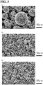
- Fig. 3(a) shows an SEM image of the raw material powder in Experimental Example 1-3
- Fig. 3(b) shows an SEM image of the raw material powder in Experimental Example 3-3
- Fig. 3(c) shows an SEM image of the raw material powder in Experimental Example 4-3.
- the raw material powder in Experimental Example 1-3 was spherical.
- coarse teardrop-shaped Cu powder and fine spherical CuZr or ZrH 2 powder coexisted.
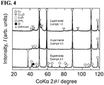
- Fig. 4 shows the results of X-ray diffraction measurements on the raw material powders in Experimental Examples 1-3, 3-3, and 4-3.
- Fig. 5 shows cross-sectional SEM-BEI images in Experimental Examples 1 to 4.
- Each structure in Experimental Example 1 contained two phases, i.e., the Cu phase and the Cu-Zr-based compound phase (mainly the Cu 5 Zr phase), and contained no eutectic phase, and crystals with a size of 10 ⁇ m or less in cross section were dispersed in the structure.
- the particle diameter of the Cu-Zr-based compound in cross section was small, and the structures were relatively uniform.
- a relatively large second phase was dispersed in the ⁇ -Cu matrix phase.
- Fig. 6 shows the results of electrical conductivity measurements on the copper alloys in Experimental Examples 1 to 4.
- the copper alloys in Experimental Examples 1 to 4 had different structures as described above. However, no large difference in tendency of electrical conductivity versus the content of Zr was found for the copper alloys in Experimental Examples 1 to 4. This may be because the electrical conductivities of the copper alloys depend on their Cu phases and there in no structural difference among the Cu phases.
- the mechanical strength of a copper alloy may depend on its Cu-Zr-based compound phase. Since a Cu-Zr-based compound phase is present in each of Experimental Examples 2 to 4, it is inferred that the value of the mechanical strength is relatively high in each of Experimental Examples 2 to 4.
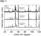
- Fig. 7 shows the results of X-ray diffraction measurements in Experimental Examples 1-3, 3-3, and 4-3. As shown in Fig.
- Fig. 8 shows cross-sectional SEM-BEI images in Experimental Example 3-1.
- Fig. 9 shows cross-sectional SEM-BEI images in Experimental Example 3-2.
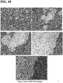
- Fig. 10 shows cross-sectional SEM-BEI images in Experimental Example 3-3.
- the average particle diameters D50 of the second phase in the SEM photographs taken were determined.
- the average particle diameters of the second phase were determined as follows. A backscattered electron image was observed at 100X to 500X, and the diameters of inscribed circles of particles in the image were determined and used as the diameters of the particles. Specifically, the diameters of all the particles present in the field of view were determined. This procedure was repeated for five fields of view.
- the particle diameters obtained were used to determine a cumulative distribution, and its median diameter was used as the average particle diameter D50.
- the average particle diameter D50 of the second phase in cross section was within the range of 1 ⁇ m to 100 ⁇ m. It was inferred that, in the second phase, an oxide film was formed in the outermost shell of each coarse particle. It was found that, in the core of the second phase, many distorted particles formed twin crystals.
- Fig. 11 shows a cross-sectional SEM-BEI image and the results of EDX measurements in Experimental Example 3-3. Fig.
- FIG. 12 shows cross-sectional SEM-BEI images, a cross-sectional STEM-BF image, the results of EDX analysis, and NBD patterns in Experimental Example 3-3.
- Fig. 13 shows a cross-sectional STEM-BF image, the results of EDX analysis, and NBD patterns in Experimental Example 3-3.
- the second phase had: an outer shell composed of a Cu-Zr-based compound phase containing Cu 5 Zr; and a core including a Zr-rich Zr phase containing 10 at% or less of Cu.
- Fig. 14 shows the results of nano-electron beam diffraction analysis at points 1 and 4 shown in Fig. 13 . As shown in Fig. 13 , in a light color fine particle, Zr was 94 at%, and this particle was found to be the Zr phase. In a color striped portion, Cu was 85 at%, and Zr was 15 at%. This portion was expected to be the Cu 5 Zr phase. As shown in Fig.
- points 1 to 3 were expected to be the Zr phase containing at least 92 at% of Zr, and points 4 and 5 were expected to be the Cu 5 Zr phase. Judging from the results of the nano-electron beam diffraction and the elementary analysis shown Fig. 14 , the Zr phase at point 1 may be an ⁇ -Zr phase. Point 4 was confirmed to be the Cu 5 Zr phase.
- Fig. 15 shows the results of measurements of hardness H by a nano-indentation method.
- the Young's modulus E and the hardness H were measured at multiple points. After the measurements, measurement points indented into the Zr phase were selected by SEM observation. The Young's modulus E and the hardness H by the nano-indentation method were determined from the measurement results.
- Fig. 16 shows the results of EBSD analysis in Experimental Example 3-3.
- Fig. 16 shows the results at point 1 (the Cu-Zr-based compound phase in the second phase) in an SEM image, point 2 (the Zr-rich Zr phase inside the Cu-Zr-based compound phase) in the SEM image, and point 3 (the Zr-rich Zr phase inside the Cu-Zr-based compound phase at a different region) in the SEM image.
- Fig. 16 also shows the results of crystal structure fitting for point 2 using the channeling pattern of Kikuchi lines. Different patterns were observed at points 1, 2, and 3, and the crystal orientations at these points were different from each other.
- Figs. 17 and 18 show crystal orientation maps by the EBSD method in Experimental Example 3-3.
- the crystal orientation maps were displayed using OIM (Orientation Imaging Microscopy) software manufactured by TSL Solutions.
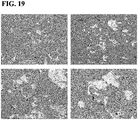
- Fig. 19 shows cross-sectional SEM-BEI images in Experimental Example 4-1.
- Fig. 20 shows cross-sectional SEM-BEI images in Experimental Example 4-2.
- Fig. 21 shows cross-sectional SEM-BEI images in Experimental Example 4-3.
- the average particle diameters D50 of the second phase in the SEM photographs taken were determined in the same manner as described above. As shown in the SEM photographs in Figs. 19 and 20 , in each of the copper alloys in Experimental Example 4, the average particle diameter D50 of the second phase in cross section was within the range of 1 ⁇ m to 100 ⁇ m.
- the second phase was in the form of coarse particle having an outer shell composed of the Cu-Zr-based compound phase containing Cu 5 Zr and a core including the Zr-rich Zr phase ( Fig. 21 ).
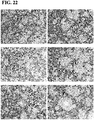
- Fig. 22 shows cross-sectional SEM-BEI images of copper alloys having the same composition as in Experimental Example 4-3 and prepared using different SPS temperatures and times. It was found that, when the SPS process was performed at 925°C for 5 minutes, a Zr phase was generated.
- Fig. 23 shows a cross-sectional SEM-BEI image and elemental maps by the EDX method in Experimental Example 4. As shown in Fig.
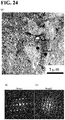
- Fig. 24(a) shows a cross-sectional TEM-BF image in Experimental Example 4-3.
- Fig. 24(b) shows an SAD pattern of Area 1
- Fig. 24(c) shows an SAD pattern of Area 2.
- a microstructure including twin crystals was also observed in the Cu 5 Zr compound phase in the SPS materiel shown in Fig. 24.
- Fig. 24(b) shows an SAD (Selected Area Diffraction) pattern of Area 1 in the microstructure shown in Fig. 24(a)
- Fig. 24(c) shows an SAD pattern of Area 2 in the microstructure shown in Fig.
- the selected-area aperture was 200 nm.
- EDX analysis was also performed at the central portions of these Areas. The results showed that the microstructure observed in Area 1 was a Zr-rich phase containing 5 at% of Cu similar to that in the SPS materials in Experimental Example 3 and three lattice spacings measured agreed with those of the ⁇ -Zr phase within 1.2%.
- the compound phase in Area 2 was the same Cu 5 Zr compound phase as that in the SPS materials in Experimental Examples 1 and 3.
- FIG. 25 shows an SEM-BEI image of the copper alloy in Experimental Example 1-3 that was obtained by subjecting a Cu-Zr-based alloy powder to SPS.
- Fig. 26 shows a cross-sectional SEM-BEI image and elemental maps by the EDX method in Experimental Example 2-3.
- this copper alloy produced using Cu powder and Zr powder had a structure in which relatively large domains of the second phase were dispersed in the ⁇ -Cu matrix phase.
- the second phase had an outer shell composed of a Cu-Zr-based compound phase containing Cu 5 Zr and a core including a Zr-rich Zr phase.
- the Zr powder remained present even after the sintering step.
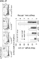
- FIG. 27 shows the results of the pin-on-disk sliding wear test (according to JIS K7218) in Experimental Example 1.
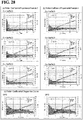
- Fig. 28 shows the results of the pin-on-disk sliding wear test in Experimental Examples 3 and 4.
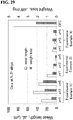
- Fig. 29 summarizes the results of the pin-on-disk sliding wear test in Experimental Examples 1, 3, and 4.
- the pin-on-disk sliding wear test was performed as follows. A test pin having a diameter of 2 mm and a height of 8 mm was cut from one of the SPS materials in the Experimental Examples, and the cut test pin was brought into contact with a S45-made disk rotated at 200 rpm.
- Daphne Super Hydro 46A mineral oil manufactured by Idemitsu Kosan Co., Ltd. was dropped onto the rotating disk.
- the test was performed as follows. A contact pressure of 2 MPa was applied, and this state was maintained for 1 minute. Then the contact pressure was increased to 20 MPa in steps of 1 MPa. Each time after the contact pressure was increased, the resulting state was maintained for 1 minute. Then (a) a change in friction coefficient, (b) the wear length of the pin after the test, and (c) the weight loss by wear were measured three times, and the averages were determined.
- the pin-on-disk sliding wear test was also performed on OFC (oxygen-free copper: JIS C1020) as a Comparative Example. As shown in Fig.
- the present invention is usable in technical fields of manufacturing of copper alloys.
Landscapes
- Chemical & Material Sciences (AREA)
- Engineering & Computer Science (AREA)
- Mechanical Engineering (AREA)
- Materials Engineering (AREA)
- Metallurgy (AREA)
- Organic Chemistry (AREA)
- Physics & Mathematics (AREA)
- Optics & Photonics (AREA)
- Manufacturing & Machinery (AREA)
- Powder Metallurgy (AREA)
- Manufacture Of Metal Powder And Suspensions Thereof (AREA)
Applications Claiming Priority (3)
| Application Number | Priority Date | Filing Date | Title |
|---|---|---|---|
| US201562165366P | 2015-05-22 | 2015-05-22 | |
| JP2015204590 | 2015-10-16 | ||
| PCT/JP2016/057847 WO2016189929A1 (fr) | 2015-05-22 | 2016-03-11 | Procédé de fabrication d'alliage de cuivre et alliage de cuivre |
Publications (3)
| Publication Number | Publication Date |
|---|---|
| EP3135780A1 true EP3135780A1 (fr) | 2017-03-01 |
| EP3135780A4 EP3135780A4 (fr) | 2018-01-31 |
| EP3135780B1 EP3135780B1 (fr) | 2020-06-17 |
Family
ID=57394212
Family Applications (1)
| Application Number | Title | Priority Date | Filing Date |
|---|---|---|---|
| EP16794497.4A Not-in-force EP3135780B1 (fr) | 2015-05-22 | 2016-03-11 | Procédé de fabrication d'alliage de cuivre et alliage de cuivre |
Country Status (6)
| Country | Link |
|---|---|
| US (1) | US10557184B2 (fr) |
| EP (1) | EP3135780B1 (fr) |
| JP (1) | JP6482092B2 (fr) |
| KR (1) | KR102468099B1 (fr) |
| CN (1) | CN106661671A (fr) |
| WO (1) | WO2016189929A1 (fr) |
Cited By (6)
| Publication number | Priority date | Publication date | Assignee | Title |
|---|---|---|---|---|
| EP3461921A4 (fr) * | 2016-12-01 | 2020-01-22 | NGK Insulators, Ltd. | Élément support éléctroconduteur et procédé de fabrication d'un tel élément support éléctroconduteur |
| EP3674016A4 (fr) * | 2017-08-21 | 2020-12-16 | JX Nippon Mining & Metals Corporation | Poudre d'alliage de cuivre destinée au formage par stratification, procédé de production de produit formé par stratification, et produit formé par stratification |
| CN112553499A (zh) * | 2020-12-04 | 2021-03-26 | 天津大学 | 一种CuCrZr/WC复合材料、制备方法及其应用 |
| EP3718665A4 (fr) * | 2017-11-28 | 2021-08-25 | NGK Insulators, Ltd. | Élément d'extrémité conducteur et procédé de fabrication s'y rapportant |
| EP3804879A4 (fr) * | 2018-06-01 | 2021-12-08 | Sanyo Special Steel Co., Ltd. | Poudre d'alliage à base de cuivre |
| US11987870B2 (en) | 2019-07-23 | 2024-05-21 | Sanyo Special Steel Co., Ltd. | Cu-based alloy powder |
Families Citing this family (9)
| Publication number | Priority date | Publication date | Assignee | Title |
|---|---|---|---|---|
| KR20190048872A (ko) * | 2017-10-31 | 2019-05-09 | 엘티씨 (주) | 고체산화물 연료전지 금속분리판용 코팅 조성물 및 그 제조방법 |
| CN109930021B (zh) * | 2017-12-19 | 2021-01-05 | 有研工程技术研究院有限公司 | 一种铜基二氧化硅复合材料及其制备方法 |
| CN110270683B (zh) * | 2018-03-16 | 2022-01-04 | 武汉理工大学 | 一种Fe/ZrH2纳米晶复合粒子及其制备方法和应用 |
| CN108441671A (zh) * | 2018-03-26 | 2018-08-24 | 中国人民解放军陆军装甲兵学院 | 一种五元铜基复合材料及制备工艺 |
| CN108728687A (zh) * | 2018-05-08 | 2018-11-02 | 湖州吴兴锐质自动化输送设备厂(普通合伙) | 一种高硬度表面镀铜的铜合金 |
| TWI674326B (zh) * | 2018-11-19 | 2019-10-11 | 財團法人工業技術研究院 | 銅鋯合金散熱元件及銅鋯合金殼體的製造方法 |
| CN110218901B (zh) * | 2019-07-04 | 2020-12-11 | 江西理工大学 | 双晶碳化钨协同增强铜基复合材料及其制备方法 |
| CN116046825B (zh) * | 2023-04-03 | 2023-06-27 | 中国核动力研究设计院 | 辐照后弥散燃料纳米压痕试样及其制备方法 |
| CN119144866B (zh) * | 2024-11-21 | 2025-05-16 | 西安稀有金属材料研究院有限公司 | 一种低密度高导热铜基石墨热沉材料的制备方法 |
Family Cites Families (5)
| Publication number | Priority date | Publication date | Assignee | Title |
|---|---|---|---|---|
| JPH03166329A (ja) * | 1989-11-24 | 1991-07-18 | Ishikawajima Harima Heavy Ind Co Ltd | 粒子分散強化Cu―Zr合金およびその製造方法 |
| JP6010413B2 (ja) | 2012-09-27 | 2016-10-19 | 東芝ホクト電子株式会社 | サーマルプリントヘッドおよびその製造方法 |
| WO2014069318A1 (fr) | 2012-11-01 | 2014-05-08 | 日本碍子株式会社 | Alliage de cuivre et son procédé de fabrication |
| CN104871262A (zh) * | 2012-11-29 | 2015-08-26 | 日本碍子株式会社 | 电压非线性电阻元件 |
| CN104164587B (zh) * | 2014-08-01 | 2016-02-10 | 烟台万隆真空冶金股份有限公司 | 一种致密的弥散强化铜基复合材料 |
-
2016
- 2016-03-11 JP JP2016569086A patent/JP6482092B2/ja active Active
- 2016-03-11 EP EP16794497.4A patent/EP3135780B1/fr not_active Not-in-force
- 2016-03-11 KR KR1020167032737A patent/KR102468099B1/ko active Active
- 2016-03-11 WO PCT/JP2016/057847 patent/WO2016189929A1/fr not_active Ceased
- 2016-03-11 CN CN201680001471.1A patent/CN106661671A/zh active Pending
- 2016-11-21 US US15/356,960 patent/US10557184B2/en active Active
Cited By (10)
| Publication number | Priority date | Publication date | Assignee | Title |
|---|---|---|---|---|
| EP3461921A4 (fr) * | 2016-12-01 | 2020-01-22 | NGK Insulators, Ltd. | Élément support éléctroconduteur et procédé de fabrication d'un tel élément support éléctroconduteur |
| US11608545B2 (en) | 2016-12-01 | 2023-03-21 | Ngk Insulators, Ltd. | Conductive supporting member and method for producing the same |
| EP3674016A4 (fr) * | 2017-08-21 | 2020-12-16 | JX Nippon Mining & Metals Corporation | Poudre d'alliage de cuivre destinée au formage par stratification, procédé de production de produit formé par stratification, et produit formé par stratification |
| EP3718665A4 (fr) * | 2017-11-28 | 2021-08-25 | NGK Insulators, Ltd. | Élément d'extrémité conducteur et procédé de fabrication s'y rapportant |
| US11511368B2 (en) | 2017-11-28 | 2022-11-29 | Ngk Insulators, Ltd. | Electrically conductive tip member and method for producing the same |
| EP3804879A4 (fr) * | 2018-06-01 | 2021-12-08 | Sanyo Special Steel Co., Ltd. | Poudre d'alliage à base de cuivre |
| US11976344B2 (en) | 2018-06-01 | 2024-05-07 | Sanyo Special Steel Co., Ltd. | Cu-based alloy powder |
| US11987870B2 (en) | 2019-07-23 | 2024-05-21 | Sanyo Special Steel Co., Ltd. | Cu-based alloy powder |
| CN112553499A (zh) * | 2020-12-04 | 2021-03-26 | 天津大学 | 一种CuCrZr/WC复合材料、制备方法及其应用 |
| CN112553499B (zh) * | 2020-12-04 | 2021-11-16 | 天津大学 | 一种CuCrZr/WC复合材料、制备方法及其应用 |
Also Published As
| Publication number | Publication date |
|---|---|
| EP3135780B1 (fr) | 2020-06-17 |
| JP6482092B2 (ja) | 2019-03-13 |
| KR102468099B1 (ko) | 2022-11-16 |
| US20170130299A1 (en) | 2017-05-11 |
| JPWO2016189929A1 (ja) | 2018-02-22 |
| EP3135780A4 (fr) | 2018-01-31 |
| KR20180009685A (ko) | 2018-01-29 |
| US10557184B2 (en) | 2020-02-11 |
| WO2016189929A1 (fr) | 2016-12-01 |
| CN106661671A (zh) | 2017-05-10 |
Similar Documents
| Publication | Publication Date | Title |
|---|---|---|
| EP3135780B1 (fr) | Procédé de fabrication d'alliage de cuivre et alliage de cuivre | |
| EP3415652B1 (fr) | Élément d'alliage, procédé de production dudit élément d'alliage, et produit comprenant ledit élément d'alliage | |
| EP3392359A1 (fr) | Élément en alliage à haute entropie, procédé de production d'un élément en alliage et produit utilisant l'élément en alliage | |
| EP4005700B1 (fr) | Poudre d'alliage à base de cuivre | |
| CN104145043A (zh) | Fe-Co系合金溅射靶材及其制造方法 | |
| Muñoz et al. | Microstructural and mechanical characteristics of W–2Ti and W–1TiC processed by hot isostatic pressing | |
| US20250083227A1 (en) | Copper alloy powder for lamination shaping, lamination shaped product production method, and lamination shaped product | |
| EP3950177B1 (fr) | Alliage à base de ni, poudre d'alliage à base de ni, élément d'alliage à base de ni et produit comprenant l'élément d'alliage à base de ni | |
| Rajan et al. | Nanocrystallization in magnetron sputtered Zr–Cu–Al–Ag thin film metallic glasses | |
| JP2006045587A (ja) | セラミックス−金属複合材料からなるスパッタリングターゲット材およびその製造方法 | |
| US11511368B2 (en) | Electrically conductive tip member and method for producing the same | |
| Průša et al. | Application of SPS consolidation and its influence on the properties of the FeAl20Si20 alloys prepared by mechanical alloying | |
| US11608545B2 (en) | Conductive supporting member and method for producing the same | |
| CN102575321B (zh) | 添加Ta的Ni3(Si,Ti)基金属间化合物 | |
| Chen et al. | Fabrication of Ti–N and Ti–Al–N Coatings on Mg–Li Alloy by Surface Mechanical Nanoalloying Treatment under Nitrogen Atmosphere at Room Temperature | |
| KR20130000470A (ko) | 기계적 특성 및 내식성을 개선한 마그네슘 재료 |
Legal Events
| Date | Code | Title | Description |
|---|---|---|---|
| STAA | Information on the status of an ep patent application or granted ep patent |
Free format text: STATUS: UNKNOWN |
|
| STAA | Information on the status of an ep patent application or granted ep patent |
Free format text: STATUS: THE INTERNATIONAL PUBLICATION HAS BEEN MADE |
|
| PUAI | Public reference made under article 153(3) epc to a published international application that has entered the european phase |
Free format text: ORIGINAL CODE: 0009012 |
|
| STAA | Information on the status of an ep patent application or granted ep patent |
Free format text: STATUS: REQUEST FOR EXAMINATION WAS MADE |
|
| 17P | Request for examination filed |
Effective date: 20161122 |
|
| AK | Designated contracting states |
Kind code of ref document: A1 Designated state(s): AL AT BE BG CH CY CZ DE DK EE ES FI FR GB GR HR HU IE IS IT LI LT LU LV MC MK MT NL NO PL PT RO RS SE SI SK SM TR |
|
| AX | Request for extension of the european patent |
Extension state: BA ME |
|
| REG | Reference to a national code |
Ref country code: DE Ref legal event code: R079 Ref document number: 602016038364 Country of ref document: DE Free format text: PREVIOUS MAIN CLASS: C22C0001040000 Ipc: C22C0009000000 |
|
| A4 | Supplementary search report drawn up and despatched |
Effective date: 20180105 |
|
| RIC1 | Information provided on ipc code assigned before grant |
Ipc: B22F 1/00 20060101ALI20171222BHEP Ipc: B22F 3/105 20060101ALI20171222BHEP Ipc: B22F 9/04 20060101ALI20171222BHEP Ipc: C22C 1/04 20060101ALI20171222BHEP Ipc: B22F 3/14 20060101ALI20171222BHEP Ipc: C22C 9/00 20060101AFI20171222BHEP |
|
| DAV | Request for validation of the european patent (deleted) | ||
| DAX | Request for extension of the european patent (deleted) | ||
| STAA | Information on the status of an ep patent application or granted ep patent |
Free format text: STATUS: EXAMINATION IS IN PROGRESS |
|
| 17Q | First examination report despatched |
Effective date: 20180928 |
|
| GRAP | Despatch of communication of intention to grant a patent |
Free format text: ORIGINAL CODE: EPIDOSNIGR1 |
|
| STAA | Information on the status of an ep patent application or granted ep patent |
Free format text: STATUS: GRANT OF PATENT IS INTENDED |
|
| INTG | Intention to grant announced |
Effective date: 20200109 |
|
| GRAS | Grant fee paid |
Free format text: ORIGINAL CODE: EPIDOSNIGR3 |
|
| GRAA | (expected) grant |
Free format text: ORIGINAL CODE: 0009210 |
|
| STAA | Information on the status of an ep patent application or granted ep patent |
Free format text: STATUS: THE PATENT HAS BEEN GRANTED |
|
| AK | Designated contracting states |
Kind code of ref document: B1 Designated state(s): AL AT BE BG CH CY CZ DE DK EE ES FI FR GB GR HR HU IE IS IT LI LT LU LV MC MK MT NL NO PL PT RO RS SE SI SK SM TR |
|
| REG | Reference to a national code |
Ref country code: GB Ref legal event code: FG4D |
|
| REG | Reference to a national code |
Ref country code: CH Ref legal event code: EP |
|
| REG | Reference to a national code |
Ref country code: IE Ref legal event code: FG4D |
|
| REG | Reference to a national code |
Ref country code: DE Ref legal event code: R096 Ref document number: 602016038364 Country of ref document: DE |
|
| REG | Reference to a national code |
Ref country code: AT Ref legal event code: REF Ref document number: 1281375 Country of ref document: AT Kind code of ref document: T Effective date: 20200715 |
|
| PG25 | Lapsed in a contracting state [announced via postgrant information from national office to epo] |
Ref country code: LT Free format text: LAPSE BECAUSE OF FAILURE TO SUBMIT A TRANSLATION OF THE DESCRIPTION OR TO PAY THE FEE WITHIN THE PRESCRIBED TIME-LIMIT Effective date: 20200617 Ref country code: SE Free format text: LAPSE BECAUSE OF FAILURE TO SUBMIT A TRANSLATION OF THE DESCRIPTION OR TO PAY THE FEE WITHIN THE PRESCRIBED TIME-LIMIT Effective date: 20200617 Ref country code: GR Free format text: LAPSE BECAUSE OF FAILURE TO SUBMIT A TRANSLATION OF THE DESCRIPTION OR TO PAY THE FEE WITHIN THE PRESCRIBED TIME-LIMIT Effective date: 20200918 Ref country code: NO Free format text: LAPSE BECAUSE OF FAILURE TO SUBMIT A TRANSLATION OF THE DESCRIPTION OR TO PAY THE FEE WITHIN THE PRESCRIBED TIME-LIMIT Effective date: 20200917 Ref country code: FI Free format text: LAPSE BECAUSE OF FAILURE TO SUBMIT A TRANSLATION OF THE DESCRIPTION OR TO PAY THE FEE WITHIN THE PRESCRIBED TIME-LIMIT Effective date: 20200617 |
|
| REG | Reference to a national code |
Ref country code: LT Ref legal event code: MG4D |
|
| REG | Reference to a national code |
Ref country code: NL Ref legal event code: MP Effective date: 20200617 |
|
| PG25 | Lapsed in a contracting state [announced via postgrant information from national office to epo] |
Ref country code: LV Free format text: LAPSE BECAUSE OF FAILURE TO SUBMIT A TRANSLATION OF THE DESCRIPTION OR TO PAY THE FEE WITHIN THE PRESCRIBED TIME-LIMIT Effective date: 20200617 Ref country code: HR Free format text: LAPSE BECAUSE OF FAILURE TO SUBMIT A TRANSLATION OF THE DESCRIPTION OR TO PAY THE FEE WITHIN THE PRESCRIBED TIME-LIMIT Effective date: 20200617 Ref country code: RS Free format text: LAPSE BECAUSE OF FAILURE TO SUBMIT A TRANSLATION OF THE DESCRIPTION OR TO PAY THE FEE WITHIN THE PRESCRIBED TIME-LIMIT Effective date: 20200617 Ref country code: BG Free format text: LAPSE BECAUSE OF FAILURE TO SUBMIT A TRANSLATION OF THE DESCRIPTION OR TO PAY THE FEE WITHIN THE PRESCRIBED TIME-LIMIT Effective date: 20200917 |
|
| REG | Reference to a national code |
Ref country code: AT Ref legal event code: MK05 Ref document number: 1281375 Country of ref document: AT Kind code of ref document: T Effective date: 20200617 |
|
| PG25 | Lapsed in a contracting state [announced via postgrant information from national office to epo] |
Ref country code: NL Free format text: LAPSE BECAUSE OF FAILURE TO SUBMIT A TRANSLATION OF THE DESCRIPTION OR TO PAY THE FEE WITHIN THE PRESCRIBED TIME-LIMIT Effective date: 20200617 Ref country code: AL Free format text: LAPSE BECAUSE OF FAILURE TO SUBMIT A TRANSLATION OF THE DESCRIPTION OR TO PAY THE FEE WITHIN THE PRESCRIBED TIME-LIMIT Effective date: 20200617 |
|
| PG25 | Lapsed in a contracting state [announced via postgrant information from national office to epo] |
Ref country code: CZ Free format text: LAPSE BECAUSE OF FAILURE TO SUBMIT A TRANSLATION OF THE DESCRIPTION OR TO PAY THE FEE WITHIN THE PRESCRIBED TIME-LIMIT Effective date: 20200617 Ref country code: RO Free format text: LAPSE BECAUSE OF FAILURE TO SUBMIT A TRANSLATION OF THE DESCRIPTION OR TO PAY THE FEE WITHIN THE PRESCRIBED TIME-LIMIT Effective date: 20200617 Ref country code: ES Free format text: LAPSE BECAUSE OF FAILURE TO SUBMIT A TRANSLATION OF THE DESCRIPTION OR TO PAY THE FEE WITHIN THE PRESCRIBED TIME-LIMIT Effective date: 20200617 Ref country code: PT Free format text: LAPSE BECAUSE OF FAILURE TO SUBMIT A TRANSLATION OF THE DESCRIPTION OR TO PAY THE FEE WITHIN THE PRESCRIBED TIME-LIMIT Effective date: 20201019 Ref country code: IT Free format text: LAPSE BECAUSE OF FAILURE TO SUBMIT A TRANSLATION OF THE DESCRIPTION OR TO PAY THE FEE WITHIN THE PRESCRIBED TIME-LIMIT Effective date: 20200617 Ref country code: SM Free format text: LAPSE BECAUSE OF FAILURE TO SUBMIT A TRANSLATION OF THE DESCRIPTION OR TO PAY THE FEE WITHIN THE PRESCRIBED TIME-LIMIT Effective date: 20200617 Ref country code: AT Free format text: LAPSE BECAUSE OF FAILURE TO SUBMIT A TRANSLATION OF THE DESCRIPTION OR TO PAY THE FEE WITHIN THE PRESCRIBED TIME-LIMIT Effective date: 20200617 Ref country code: EE Free format text: LAPSE BECAUSE OF FAILURE TO SUBMIT A TRANSLATION OF THE DESCRIPTION OR TO PAY THE FEE WITHIN THE PRESCRIBED TIME-LIMIT Effective date: 20200617 |
|
| PG25 | Lapsed in a contracting state [announced via postgrant information from national office to epo] |
Ref country code: PL Free format text: LAPSE BECAUSE OF FAILURE TO SUBMIT A TRANSLATION OF THE DESCRIPTION OR TO PAY THE FEE WITHIN THE PRESCRIBED TIME-LIMIT Effective date: 20200617 Ref country code: SK Free format text: LAPSE BECAUSE OF FAILURE TO SUBMIT A TRANSLATION OF THE DESCRIPTION OR TO PAY THE FEE WITHIN THE PRESCRIBED TIME-LIMIT Effective date: 20200617 Ref country code: IS Free format text: LAPSE BECAUSE OF FAILURE TO SUBMIT A TRANSLATION OF THE DESCRIPTION OR TO PAY THE FEE WITHIN THE PRESCRIBED TIME-LIMIT Effective date: 20201017 |
|
| REG | Reference to a national code |
Ref country code: DE Ref legal event code: R097 Ref document number: 602016038364 Country of ref document: DE |
|
| PLBE | No opposition filed within time limit |
Free format text: ORIGINAL CODE: 0009261 |
|
| STAA | Information on the status of an ep patent application or granted ep patent |
Free format text: STATUS: NO OPPOSITION FILED WITHIN TIME LIMIT |
|
| PG25 | Lapsed in a contracting state [announced via postgrant information from national office to epo] |
Ref country code: DK Free format text: LAPSE BECAUSE OF FAILURE TO SUBMIT A TRANSLATION OF THE DESCRIPTION OR TO PAY THE FEE WITHIN THE PRESCRIBED TIME-LIMIT Effective date: 20200617 |
|
| 26N | No opposition filed |
Effective date: 20210318 |
|
| PG25 | Lapsed in a contracting state [announced via postgrant information from national office to epo] |
Ref country code: SI Free format text: LAPSE BECAUSE OF FAILURE TO SUBMIT A TRANSLATION OF THE DESCRIPTION OR TO PAY THE FEE WITHIN THE PRESCRIBED TIME-LIMIT Effective date: 20200617 |
|
| PG25 | Lapsed in a contracting state [announced via postgrant information from national office to epo] |
Ref country code: MC Free format text: LAPSE BECAUSE OF FAILURE TO SUBMIT A TRANSLATION OF THE DESCRIPTION OR TO PAY THE FEE WITHIN THE PRESCRIBED TIME-LIMIT Effective date: 20200617 |
|
| REG | Reference to a national code |
Ref country code: CH Ref legal event code: PL |
|
| REG | Reference to a national code |
Ref country code: BE Ref legal event code: MM Effective date: 20210331 |
|
| PG25 | Lapsed in a contracting state [announced via postgrant information from national office to epo] |
Ref country code: IE Free format text: LAPSE BECAUSE OF NON-PAYMENT OF DUE FEES Effective date: 20210311 Ref country code: LU Free format text: LAPSE BECAUSE OF NON-PAYMENT OF DUE FEES Effective date: 20210311 Ref country code: LI Free format text: LAPSE BECAUSE OF NON-PAYMENT OF DUE FEES Effective date: 20210331 Ref country code: CH Free format text: LAPSE BECAUSE OF NON-PAYMENT OF DUE FEES Effective date: 20210331 |
|
| PG25 | Lapsed in a contracting state [announced via postgrant information from national office to epo] |
Ref country code: BE Free format text: LAPSE BECAUSE OF NON-PAYMENT OF DUE FEES Effective date: 20210331 |
|
| PG25 | Lapsed in a contracting state [announced via postgrant information from national office to epo] |
Ref country code: HU Free format text: LAPSE BECAUSE OF FAILURE TO SUBMIT A TRANSLATION OF THE DESCRIPTION OR TO PAY THE FEE WITHIN THE PRESCRIBED TIME-LIMIT; INVALID AB INITIO Effective date: 20160311 |
|
| PG25 | Lapsed in a contracting state [announced via postgrant information from national office to epo] |
Ref country code: CY Free format text: LAPSE BECAUSE OF FAILURE TO SUBMIT A TRANSLATION OF THE DESCRIPTION OR TO PAY THE FEE WITHIN THE PRESCRIBED TIME-LIMIT Effective date: 20200617 |
|
| PG25 | Lapsed in a contracting state [announced via postgrant information from national office to epo] |
Ref country code: MK Free format text: LAPSE BECAUSE OF FAILURE TO SUBMIT A TRANSLATION OF THE DESCRIPTION OR TO PAY THE FEE WITHIN THE PRESCRIBED TIME-LIMIT Effective date: 20200617 |
|
| PGFP | Annual fee paid to national office [announced via postgrant information from national office to epo] |
Ref country code: DE Payment date: 20240130 Year of fee payment: 9 Ref country code: GB Payment date: 20240201 Year of fee payment: 9 |
|
| PGFP | Annual fee paid to national office [announced via postgrant information from national office to epo] |
Ref country code: FR Payment date: 20240213 Year of fee payment: 9 |
|
| PG25 | Lapsed in a contracting state [announced via postgrant information from national office to epo] |
Ref country code: TR Free format text: LAPSE BECAUSE OF FAILURE TO SUBMIT A TRANSLATION OF THE DESCRIPTION OR TO PAY THE FEE WITHIN THE PRESCRIBED TIME-LIMIT Effective date: 20200617 |
|
| PG25 | Lapsed in a contracting state [announced via postgrant information from national office to epo] |
Ref country code: MT Free format text: LAPSE BECAUSE OF FAILURE TO SUBMIT A TRANSLATION OF THE DESCRIPTION OR TO PAY THE FEE WITHIN THE PRESCRIBED TIME-LIMIT Effective date: 20200617 |
|
| REG | Reference to a national code |
Ref country code: DE Ref legal event code: R119 Ref document number: 602016038364 Country of ref document: DE |
|
| GBPC | Gb: european patent ceased through non-payment of renewal fee |
Effective date: 20250311 |
|
| PG25 | Lapsed in a contracting state [announced via postgrant information from national office to epo] |
Ref country code: DE Free format text: LAPSE BECAUSE OF NON-PAYMENT OF DUE FEES Effective date: 20251001 |
|
| PG25 | Lapsed in a contracting state [announced via postgrant information from national office to epo] |
Ref country code: GB Free format text: LAPSE BECAUSE OF NON-PAYMENT OF DUE FEES Effective date: 20250311 |
|
| PG25 | Lapsed in a contracting state [announced via postgrant information from national office to epo] |
Ref country code: FR Free format text: LAPSE BECAUSE OF NON-PAYMENT OF DUE FEES Effective date: 20250331 |