EP3136268A1 - Procede d'analyse de securite d'un circuit logique - Google Patents
Procede d'analyse de securite d'un circuit logique Download PDFInfo
- Publication number
- EP3136268A1 EP3136268A1 EP15183113.8A EP15183113A EP3136268A1 EP 3136268 A1 EP3136268 A1 EP 3136268A1 EP 15183113 A EP15183113 A EP 15183113A EP 3136268 A1 EP3136268 A1 EP 3136268A1
- Authority
- EP
- European Patent Office
- Prior art keywords
- attack
- security
- component
- data
- channel
- Prior art date
- Legal status (The legal status is an assumption and is not a legal conclusion. Google has not performed a legal analysis and makes no representation as to the accuracy of the status listed.)
- Granted
Links
Images


Classifications
-
- G—PHYSICS
- G06—COMPUTING OR CALCULATING; COUNTING
- G06F—ELECTRIC DIGITAL DATA PROCESSING
- G06F30/00—Computer-aided design [CAD]
- G06F30/30—Circuit design
- G06F30/36—Circuit design at the analogue level
- G06F30/367—Design verification, e.g. using simulation, simulation program with integrated circuit emphasis [SPICE], direct methods or relaxation methods
-
- G—PHYSICS
- G06—COMPUTING OR CALCULATING; COUNTING
- G06F—ELECTRIC DIGITAL DATA PROCESSING
- G06F21/00—Security arrangements for protecting computers, components thereof, programs or data against unauthorised activity
- G06F21/50—Monitoring users, programs or devices to maintain the integrity of platforms, e.g. of processors, firmware or operating systems
- G06F21/55—Detecting local intrusion or implementing counter-measures
- G06F21/552—Detecting local intrusion or implementing counter-measures involving long-term monitoring or reporting
-
- G—PHYSICS
- G06—COMPUTING OR CALCULATING; COUNTING
- G06F—ELECTRIC DIGITAL DATA PROCESSING
- G06F21/00—Security arrangements for protecting computers, components thereof, programs or data against unauthorised activity
- G06F21/50—Monitoring users, programs or devices to maintain the integrity of platforms, e.g. of processors, firmware or operating systems
- G06F21/57—Certifying or maintaining trusted computer platforms, e.g. secure boots or power-downs, version controls, system software checks, secure updates or assessing vulnerabilities
- G06F21/577—Assessing vulnerabilities and evaluating computer system security
-
- G—PHYSICS
- G06—COMPUTING OR CALCULATING; COUNTING
- G06F—ELECTRIC DIGITAL DATA PROCESSING
- G06F21/00—Security arrangements for protecting computers, components thereof, programs or data against unauthorised activity
- G06F21/70—Protecting specific internal or peripheral components, in which the protection of a component leads to protection of the entire computer
- G06F21/71—Protecting specific internal or peripheral components, in which the protection of a component leads to protection of the entire computer to assure secure computing or processing of information
- G06F21/76—Protecting specific internal or peripheral components, in which the protection of a component leads to protection of the entire computer to assure secure computing or processing of information in application-specific integrated circuits [ASIC] or field-programmable devices, e.g. field-programmable gate arrays [FPGA] or programmable logic devices [PLD]
-
- G—PHYSICS
- G06—COMPUTING OR CALCULATING; COUNTING
- G06F—ELECTRIC DIGITAL DATA PROCESSING
- G06F30/00—Computer-aided design [CAD]
- G06F30/30—Circuit design
-
- G—PHYSICS
- G06—COMPUTING OR CALCULATING; COUNTING
- G06F—ELECTRIC DIGITAL DATA PROCESSING
- G06F30/00—Computer-aided design [CAD]
- G06F30/30—Circuit design
- G06F30/32—Circuit design at the digital level
- G06F30/33—Design verification, e.g. functional simulation or model checking
-
- G—PHYSICS
- G06—COMPUTING OR CALCULATING; COUNTING
- G06F—ELECTRIC DIGITAL DATA PROCESSING
- G06F30/00—Computer-aided design [CAD]
- G06F30/30—Circuit design
- G06F30/32—Circuit design at the digital level
- G06F30/33—Design verification, e.g. functional simulation or model checking
- G06F30/3308—Design verification, e.g. functional simulation or model checking using simulation
-
- G—PHYSICS
- G06—COMPUTING OR CALCULATING; COUNTING
- G06F—ELECTRIC DIGITAL DATA PROCESSING
- G06F30/00—Computer-aided design [CAD]
- G06F30/30—Circuit design
- G06F30/34—Circuit design for reconfigurable circuits, e.g. field programmable gate arrays [FPGA] or programmable logic devices [PLD]
-
- G—PHYSICS
- G06—COMPUTING OR CALCULATING; COUNTING
- G06F—ELECTRIC DIGITAL DATA PROCESSING
- G06F30/00—Computer-aided design [CAD]
- G06F30/30—Circuit design
- G06F30/39—Circuit design at the physical level
- G06F30/398—Design verification or optimisation, e.g. using design rule check [DRC], layout versus schematics [LVS] or finite element methods [FEM]
-
- G—PHYSICS
- G06—COMPUTING OR CALCULATING; COUNTING
- G06F—ELECTRIC DIGITAL DATA PROCESSING
- G06F21/00—Security arrangements for protecting computers, components thereof, programs or data against unauthorised activity
- G06F21/50—Monitoring users, programs or devices to maintain the integrity of platforms, e.g. of processors, firmware or operating systems
- G06F21/55—Detecting local intrusion or implementing counter-measures
- G06F21/554—Detecting local intrusion or implementing counter-measures involving event detection and direct action
-
- G—PHYSICS
- G06—COMPUTING OR CALCULATING; COUNTING
- G06F—ELECTRIC DIGITAL DATA PROCESSING
- G06F21/00—Security arrangements for protecting computers, components thereof, programs or data against unauthorised activity
- G06F21/50—Monitoring users, programs or devices to maintain the integrity of platforms, e.g. of processors, firmware or operating systems
- G06F21/55—Detecting local intrusion or implementing counter-measures
- G06F21/556—Detecting local intrusion or implementing counter-measures involving covert channels, i.e. data leakage between processes
-
- G—PHYSICS
- G06—COMPUTING OR CALCULATING; COUNTING
- G06F—ELECTRIC DIGITAL DATA PROCESSING
- G06F21/00—Security arrangements for protecting computers, components thereof, programs or data against unauthorised activity
- G06F21/70—Protecting specific internal or peripheral components, in which the protection of a component leads to protection of the entire computer
- G06F21/71—Protecting specific internal or peripheral components, in which the protection of a component leads to protection of the entire computer to assure secure computing or processing of information
-
- G—PHYSICS
- G06—COMPUTING OR CALCULATING; COUNTING
- G06F—ELECTRIC DIGITAL DATA PROCESSING
- G06F2221/00—Indexing scheme relating to security arrangements for protecting computers, components thereof, programs or data against unauthorised activity
- G06F2221/03—Indexing scheme relating to G06F21/50, monitoring users, programs or devices to maintain the integrity of platforms
- G06F2221/034—Test or assess a computer or a system
-
- G—PHYSICS
- G06—COMPUTING OR CALCULATING; COUNTING
- G06F—ELECTRIC DIGITAL DATA PROCESSING
- G06F30/00—Computer-aided design [CAD]
Definitions
- the present invention relates generally to the field of electronic logic circuits, in particular integrated circuits, e.g. the so-called application-specific, integrated circuits or ASICs, the so-called field programmable gate arrays or FPGAs and the so-called system-on-chip systems. More particularly, the present invention relates to a method of analyzing a logic circuit that includes a plurality of components and channels for exchanging data between components, wherein functional characteristics are assigned to simulate operation of the logic circuit of each component and each channel in a circuit model ,
- Logical circuits are used in numerous electrical and electronic devices or systems. Such circuits typically include a substrate (eg, a semiconductor substrate) on which different devices or device blocks are housed and wired together. These components or component blocks are also referred to as components.
- An integrated circuit usually consists of a number of different components which are accommodated on a monocrystalline substrate. If all or a large part of the desired functions are realized on a chip, this is called a system-on-chip. This integration provides extensive functionality and applications in the smallest of spaces. With the rapid advances in technological development, it is now possible to package complex logic circuits with a large number of components on a single semiconductor chip.
- Such complex circuits are usually designed by means of computer-aided tools.
- a virtual circuit model is created in order to simulate a desired mode of operation.
- each component hardware components, system components consisting of hardware and software parts, etc.
- a functional component model to construct a circuit model of the logical circuit and the logical system, respectively.
- a functionality of the corresponding circuit can be checked and verified by means of simulation. This applies in particular to a circuit model with a high degree of abstraction, which is also referred to as a high-level model.
- the functional component models and circuit models of logical circuits can be drafted, presented and a functional behavior of the logic circuit and the individual components of the logic circuit can be simulated.
- a functional behavior of the logic circuit and the individual components of the logic circuit can be simulated.
- Maturities and / or powers of the individual function components are set as parameters, so that the circuit model behaves during a simulation as the corresponding real circuit or a real hardware model.
- the invention has the object of developing the aforementioned method in order to perform a reliable safety analysis.
- a simulation is used to perform a safety analysis with reports on the suitability of the set safety properties and on the vulnerability of a virtually executed attack. For example, if a manipulation of data in an attacked component, this manipulated data migrate through other components according to the functionality of the circuit model. Also with these components, the vulnerability of the security properties is determined as a result of processing the manipulated data. If necessary, additional security measures can subsequently be inserted or removed to optimize the system.
- each component and each channel is expanded with its own simulation unit.
- the latter then carries out the checking steps during a simulation for the respective channel or the respective component and generates a corresponding report if security risks are detected.
- event data As a result of an applied attack.
- This event data describes any manipulation of data that may be possible, allowing more accurate analysis.
- probability data are generated to determine the vulnerability of the respective security property.
- the attack report then indicates what probability the attack is successful with.
- the probability data may indicate how long the attack is likely to take until the security property concerned is violated.
- risk data for evaluating the respective security property from the probability data.
- this risk data it can be easily determined whether a security property has to be supplemented or reduced. If, for example, a tolerable risk level is defined for the circuit to be developed, the risk data is initially compared with this level of risk. For a component, if the identified risk exceeds the target, the safety feature must be supplemented. In the opposite case, this also detects an excessive security property.
- a simple development of the invention provides that an attack is selected from a previously created library. This eliminates the need to re-create an attack for each use case. Rather, an attack is modeled by simply selecting it from the library and, if necessary, adjusting attack parameters.
- each attack is / will be assigned an attack potential and / or an attack type and / or an attack time trigger.
- an attack can be selected in a simple manner or can be modeled in a modified form.
- an attack graph is modeled with multiple graph nodes and that each graph node corresponds to an attack applied to a particular component and / or channel. This adds further method steps in which additional attacks are applied to individual components or channels in accordance with the modeled attack graph, and in turn a determination of the vulnerability of the respective security properties of the affected components takes place. From the observed effects of the multiple attacks, the necessary steps for adapting the security measures can be derived.
- Another advantage is that when multiple attack graphs are linked together, so that an attack graph is executed in response to an execution progress of another attack graph. This further increases the complexity of the applicable attack scenarios. With this increasing complexity, the achievable security of the developed circuit also increases against any form of attack.
- the circuit model of the logic circuit is advantageously provided that this is designed as a high-level model, in particular as a so-called electronic system-level model.
- a so-called electronic system-level model During various steps of a logic circuit design process, particularly for ASICs, different circuit models are created with different degrees of abstraction. With these circuit models also different functionalities of the logic circuit can be tested.
- a so-called high-level model or in particular a so-called electronic system level or ESL model the logical circuit is designed.
- functionalities, algorithms, etc. of the individual components as well as the logical circuit can be modeled respectively functional models of components and circuit can be created and on the other hand the effects of attacks and the vulnerability of the set security properties can be checked efficiently.
- an integrated circuit in particular a so-called application-specific integrated circuit or a so-called system-on-chip, is provided as the logic circuit.
- An integrated circuit may consist of a combination of several electrically connected electronic components - mostly semiconductor devices (e.g., diodes, transistors, etc.) and / or other active and passive devices (e.g., resistors, etc.).
- semiconductor devices e.g., diodes, transistors, etc.
- active and passive devices e.g., resistors, etc.
- ASICs application specific integrated circuits
- a functionality of the logic circuit is already clearly defined during development and production and can not be changed afterwards. That is, an ASIC has a strict dependency on the data being processed, and the logic implemented in an ASIC is closely related to the one or more functions to be performed. Therefore, it is particularly important for ASICs that system security is determined and checked in a simple and cost-effective manner already during the design or development phase, for example, whether the required or desired risk specifications are met, for example.
- Another form of integrated circuit is the so-called system-on-chip or one-chip system.
- a system for example embedded computer, etc.
- a combination of different components e.g. logical circuits, timing, microtechnical sensors, memory units, processors, interfaces, bus system, etc.
- the method is particularly suitable, because here only more inadequate assessments of the security situation are possible with conventional methods due to the increasing system size and complexity.
- FPGAs field programmable logic gate arrays
- various circuits can be realized by a specific configuration of internal structures (eg, gates, logic blocks, etc.) - from simple circuits such as a counter circuit to highly complex circuits such as a microprocessor.
- FPGAs are used in all areas of digital technology, in particular in areas where fast signal processing and flexible changeability of the circuit are important.
- FPGAs have the advantage of lower development costs and very short implementation times.
- a particular advantage of FPGAs is that they can be reconfigured, so that a logic circuit realized with an FPGA can easily be corrected and, if necessary, can be expanded with security mechanisms.
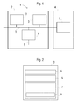
- the starting point of the present method is a virtual circuit model 1 in a suitable computer-based simulation environment.
- the circuit model 1 forms a logic circuit such as e.g.
- a system-on-chip or ASIC is implemented as a high-level model (e.g., ESL model) at the system level with a high-level programming language, such as e.g. Systems described.
- the virtual circuit model 1 in a first module 2 has three exemplary components 3 and in a second module 4, a component 3.
- These components 3 may be eg hardware components (eg electronic components, etc.) or system components (eg logic circuits, components with hardware and software components, etc.).
- a functional model also a high-level model in a programming language such eg systems.
- a functional behavior of the respective component 3 can be simulated. In this case, for example, 3 runtimes and / or services are specified as adjustable parameters for each component.
- the simulated data processing then takes place in accordance with these specifications with terms and performances that approximately correspond to the real logic circuit.
- the components 3 are interconnected with each other and with external (not shown) components through channels 5.
- a suitable bus is usually provided.
- Fig. 2 An extended with inventive attributes component 3 is in Fig. 2 shown.
- Component 3 is assigned defined security properties 6 (security properties).
- security properties 6 security properties
- known security concepts such as "confidentiality”, “integrity” (integrity), “authenticity” (authenticity) and “non-repudiation” are used, for example, in data processing.
- the security properties 6 for example, the degree of confidentiality and / or integrity and / or authenticity and / or traceability which the respective component 3 processes data is thus determined. With it finds a classification of each individual component 3 with regard to its security properties 6 for the protection of security-relevant data instead.
- defined security properties 6 determine with which degree of confidentiality and / or integrity and / or authenticity and / or traceability security-relevant data is transmitted through the respective channel 5.
- the determination of the security properties 6 takes place in such a way that in the simulation environment each component 3 and each channel 5 is linked with security parameters.
- the respective security parameter then defines e.g. as a number between 0 and 10, the degree of confidentiality and / or integrity and / or authenticity and / or traceability, etc. is determined.
- the component 3 For the processing of security-relevant data, the component 3 comprises suitable memory devices 7.
- defined security requirements 8 are defined for the security-relevant data. Specifically, these are stipulations as to what degree of confidentiality and / or integrity and / or authenticity and / or traceability is required. In this way, the security-relevant data to be processed by means of the component 3 or to be transmitted by means of a channel 5 are also classified.
- These security requirements 8 are also present in the simulation environment, e.g. by security parameters, which are linked to the data, determinable.
- security-relevant data is linked to a security status.
- This security status provides information as to whether the corresponding data is still trustworthy, for example, or whether there is a probability that a data manipulation has already taken place.
- Each component 3 of the circuit model 1 is expanded with a simulation unit 9. This first checks whether the security status and the security requirements 8 of the data processed in the respective component 3 corresponds to the security properties 6 of this component 3. For example, the data requires a high degree of confidentiality, which is why they have encryption as a security requirement 8. If such data is then processed or forwarded unencrypted, there is no correspondence between the security requirements 8 of the data and the security properties 6 of the affected component 3 or the affected channel 5. As a result of such non-correspondence, a security risk report is generated by means of the simulation unit 9 and forwarded to an output unit ,
- the modeling and application of an attack 10, 11, 12 takes place on a component 3 or a channel 5.
- the simulation unit 9 of a component 3 selects an attack 10, 11, 12 from a previously created library, shown in FIG Fig. 3 ,
- An attack 10, 11, 12 has various attack characteristics derived, for example, from the classifications "Confidentiality”, “Integrity”, “Authenticity” and “Detectability". For example, attack potential is set as an attack potential. Another marking concerns the type of attack, for example "key reconstruction”.
- an attack 10, 11, 12 is assigned an attack time trigger. The latter gives the simulation unit 9 of the respective component 3 when an attack is triggered ("armed"), whereby the Attack 10, 11, 12 depending on the configuration immediately or later.
- a triggered attack 10, 11, 12 interacts with the virtual circuit model 1.
- a respective attack 10, 11, 12 has access to data, whereby manipulation possibilities exist. Specifically, these manipulation options depend on which safety properties 6 the affected component 3 or the affected channel 5 has and which attack properties of the applied to this component 3 and this channel 5 attack 10, 11, 12 has.
- the library selects an attack 10 with Key Reconstructive properties as the attack type, High as the attack potential, and Immediately as the attack time trigger.
- these properties can be set in the simulation environment as attack parameters.
- this attack 10 Upon selection of this attack 10, it is immediately applied to an associated component 3. If this component has an encryption property with a strength level less than that of the attack potential (eg "medium"), then the attack 10 gains access to the data processed in this component 3 and can manipulate it. Accordingly, the security status of this data changes and an attack report with event data is generated and output to an output unit. There is the possibility to specify a probability for the attack success. In the security status of the data and in the attack report then appropriate probability data are given, eg that the data with a probability of 70% were manipulated.
- risk data can be derived from the probability data. For example, as a result of an attack simulation for each component 3 and each channel 5 a risk value (Security Risk Number) is issued. These risk values then provide information about how injury-prone components 3 and 5 are against the applied attacks 10-12.
- a comparison with a required level of risk shows immediately where the security measures have weak points or where unnecessary security measures have been taken. For example, by simulating a use case, it can be shown that execution of cryptographic functions is, to a lesser extent, sufficient than initially thought to protect the system.
- one or more attack graphs 14, 15 are formed, as in Fig. 4 shown.
- the execution of an attack graph 14 depends on the termination of another attack graph 15.
- the triggering of an attack graph 14, 15 applies a predetermined sequence of attacks 10, 11, 12 or 10, 13 to the circuit model 1.
- a mapping of an attack graph 14 to the circuit model 1 takes place, as in FIG Fig. 5 shown.
- This can be an attack 10-13 or multiple attacks 10-13 can be applied to one component 3 or to multiple components 3.
- attack graphs 14, 15 can be applied, whereby 10-13 security holes for the simulated application are shown by a suitable combination of attacks.
- a task can check a data packet by means of MAC control and request it again if necessary.
- the simulation unit 9 in the respective component 3 monitors the modeled circuit model 1 and reports security violations by means of corresponding reports via an output unit.
- data and data quality can be tracked and recorded during a simulation. This allows the tracking of security-relevant events.
- the effects of manipulated data on the circuit model 1 are determined.
- trusted data 16 are manipulated by attacks 10, 11.
- the circuit model 1 consists of four components 3, 3 ', 3 ", 3"', wherein a first component 3 is connected to a second component 3 'via a first bus and wherein the second component 3' via another bus with a third and a fourth component 3 ", 3"'is connected.
- a first attack 10 causes the reconstruction 17 of a key with which the first bus was previously protected.
- the data 16 routed through this channel 5 is decrypted.
- component 3 'already decrypted data 16' reach.
- This simulation action causes the security status associated with the data 16 'to change and a corresponding attack report 18 to be issued. It indicates, for example, that the data 16 routed through the named channel 5 'at a particular time was decrypted.
Landscapes
- Engineering & Computer Science (AREA)
- Computer Hardware Design (AREA)
- Theoretical Computer Science (AREA)
- Physics & Mathematics (AREA)
- General Engineering & Computer Science (AREA)
- General Physics & Mathematics (AREA)
- Computer Security & Cryptography (AREA)
- Software Systems (AREA)
- Evolutionary Computation (AREA)
- Geometry (AREA)
- Microelectronics & Electronic Packaging (AREA)
- Computing Systems (AREA)
- Mathematical Physics (AREA)
- Design And Manufacture Of Integrated Circuits (AREA)
- Tests Of Electronic Circuits (AREA)
- Management, Administration, Business Operations System, And Electronic Commerce (AREA)
Priority Applications (4)
| Application Number | Priority Date | Filing Date | Title |
|---|---|---|---|
| EP15183113.8A EP3136268B1 (fr) | 2015-08-31 | 2015-08-31 | Procede d'analyse de securite d'un circuit logique |
| IL247055A IL247055A0 (en) | 2015-08-31 | 2016-08-02 | A method for analyzing a logic circuit |
| US15/248,370 US10146937B2 (en) | 2015-08-31 | 2016-08-26 | Method for analyzing a logic circuit |
| CN201610799890.6A CN106484945B (zh) | 2015-08-31 | 2016-08-31 | 用于分析逻辑电路的方法 |
Applications Claiming Priority (1)
| Application Number | Priority Date | Filing Date | Title |
|---|---|---|---|
| EP15183113.8A EP3136268B1 (fr) | 2015-08-31 | 2015-08-31 | Procede d'analyse de securite d'un circuit logique |
Publications (2)
| Publication Number | Publication Date |
|---|---|
| EP3136268A1 true EP3136268A1 (fr) | 2017-03-01 |
| EP3136268B1 EP3136268B1 (fr) | 2019-06-19 |
Family
ID=54106140
Family Applications (1)
| Application Number | Title | Priority Date | Filing Date |
|---|---|---|---|
| EP15183113.8A Active EP3136268B1 (fr) | 2015-08-31 | 2015-08-31 | Procede d'analyse de securite d'un circuit logique |
Country Status (4)
| Country | Link |
|---|---|
| US (1) | US10146937B2 (fr) |
| EP (1) | EP3136268B1 (fr) |
| CN (1) | CN106484945B (fr) |
| IL (1) | IL247055A0 (fr) |
Families Citing this family (5)
| Publication number | Priority date | Publication date | Assignee | Title |
|---|---|---|---|---|
| AT521713B1 (de) * | 2018-10-11 | 2023-07-15 | Avl List Gmbh | Verfahren zur Detektion sicherheitsrelevanter Datenflüsse |
| EP3722942B1 (fr) * | 2019-04-10 | 2023-03-22 | The Boeing Company | Mise en oeuvre de tests d'intégration utilisant de tests d'unité |
| CN114676438B (zh) * | 2022-04-15 | 2023-06-09 | 电子科技大学 | 面向硬件系统多维脆弱性的快速探测方法 |
| CN119404189A (zh) * | 2022-04-28 | 2025-02-07 | 奥普蒂马设计自动化有限公司 | 故障攻击模拟 |
| EP4273725A1 (fr) * | 2022-05-02 | 2023-11-08 | AIT Austrian Institute of Technology GmbH | Procédé de détermination de vulnérabilités critiques |
Family Cites Families (7)
| Publication number | Priority date | Publication date | Assignee | Title |
|---|---|---|---|---|
| US6516415B1 (en) * | 1999-04-23 | 2003-02-04 | Geneticware Co., Ltd | Device and method of maintaining a secret code within an integrated circuit package |
| JP2007535718A (ja) * | 2003-07-07 | 2007-12-06 | クリプターグラフィー リサーチ インコーポレイテッド | 海賊行為を規制し、インタラクティブコンテンツを使用可能にするための再プログラマブルなセキュリティ |
| US8091050B2 (en) * | 2008-10-01 | 2012-01-03 | International Business Machines Corporation | Modeling system-level effects of soft errors |
| EP2489407A1 (fr) * | 2011-02-15 | 2012-08-22 | Koninklijke Philips Electronics N.V. | Appareil thérapeutique de réchauffement d'un sujet |
| US9449196B1 (en) * | 2013-04-22 | 2016-09-20 | Jasper Design Automation, Inc. | Security data path verification |
| US9092631B2 (en) * | 2013-10-16 | 2015-07-28 | Battelle Memorial Institute | Computer-implemented security evaluation methods, security evaluation systems, and articles of manufacture |
| US9721100B2 (en) * | 2014-06-27 | 2017-08-01 | Intel Corporation | Technologies for protected hardware function monitoring and forensics |
-
2015
- 2015-08-31 EP EP15183113.8A patent/EP3136268B1/fr active Active
-
2016
- 2016-08-02 IL IL247055A patent/IL247055A0/en active IP Right Grant
- 2016-08-26 US US15/248,370 patent/US10146937B2/en active Active
- 2016-08-31 CN CN201610799890.6A patent/CN106484945B/zh active Active
Non-Patent Citations (3)
| Title |
|---|
| JOHANNES LOINIG ET AL: "Idea: Simulation Based Security Requirement Verification for Transaction Level Models", 9 February 2011, ENGINEERING SECURE SOFTWARE AND SYSTEMS, SPRINGER BERLIN HEIDELBERG, BERLIN, HEIDELBERG, PAGE(S) 264 - 271, ISBN: 978-3-642-19124-4, XP019160353 * |
| JOHANNES LOINIG ET AL: "Towards formal system-level verification of security requirements during hardware/software codesign", SOC CONFERENCE (SOCC), 2010 IEEE INTERNATIONAL, IEEE, 27 September 2010 (2010-09-27), pages 388 - 391, XP031880663, ISBN: 978-1-4244-6682-5, DOI: 10.1109/SOCC.2010.5784702 * |
| YVES ROUDIER ET AL: "SysML-Sec: A SysML environment for the design and development of secure embedded systems", 1 January 2013 (2013-01-01), XP055249349, Retrieved from the Internet <URL:http://perso.telecom-paristech.fr/~apvrille/docs/APCOSEC2013_ApvrilleRoudier.pdf> [retrieved on 20160211] * |
Also Published As
| Publication number | Publication date |
|---|---|
| CN106484945A (zh) | 2017-03-08 |
| IL247055A0 (en) | 2016-12-29 |
| EP3136268B1 (fr) | 2019-06-19 |
| US10146937B2 (en) | 2018-12-04 |
| US20170061124A1 (en) | 2017-03-02 |
| CN106484945B (zh) | 2020-04-10 |
Similar Documents
| Publication | Publication Date | Title |
|---|---|---|
| AT522625B1 (de) | Verfahren zur Sicherheitsüberprüfung einer Technikeinheit | |
| EP3274825B1 (fr) | Procédé et environnement d'exécution pour exécuter de façon sécurisée des instructions de programme | |
| EP3136268B1 (fr) | Procede d'analyse de securite d'un circuit logique | |
| DE102021110766B3 (de) | Forensik-Modul und eingebettetes System | |
| DE102014208838A1 (de) | Verfahren zum Betreiben eines Steuergeräts | |
| EP4463784B1 (fr) | Surveillance dynamique de l'intégrité d'un environnement d'exécution de conteneur s'exécutant sur un dispositif de calcule hôte | |
| DE102016210788A1 (de) | Komponente zur Verarbeitung eines schützenswerten Datums und Verfahren zur Umsetzung einer Sicherheitsfunktion zum Schutz eines schützenswerten Datums in einer solchen Komponente | |
| DE10324594A1 (de) | Verfahren zum Bereitstellen einer verbesserten Simulationsfähigkeit eines dynamischen Systems außerhalb der ursprünglichen Modellierungsumgebung | |
| DE102018217016A1 (de) | Ein-Chip-System und Sicherheitsschaltung mit einem derartigen Ein-Chip-System | |
| EP4297334B1 (fr) | Procédé de mise en oeuvre et d'utilisation de matériau cryptographique dans au moins un composant de système d'un système informatique | |
| WO2014191178A1 (fr) | Mise à disposition de séquences de bits aléatoires dans un environnement d'exécution virtuel | |
| DE102013224365A1 (de) | Verfahren für einen sicheren Hochfahrablauf eines elektronischen Systems | |
| EP3876123B1 (fr) | Agencement et procédé de fonctionnement pour un démarrage sécurisé d'un dispositif électronique | |
| DE102021110768B3 (de) | Forensik-Modul und eingebettetes System | |
| DE102013223234A1 (de) | Zugriff auf einen Speicher | |
| EP4421622A1 (fr) | Procédé et système pour effectuer une opération d'installation pour une application sur un environnement d'exécution pendant le fonctionnement d'un système tout en vérifiant les modifications du temps de fonctionnement du système | |
| DE102017202787A1 (de) | Verfahren und Validierungseinheit zum Steuern des Ladens von in IT-Systemen, insbesondere Eingebetteten Systemen, benutzbaren Krypto-Schlüsseln, insbesondere "Key BLOBs" | |
| DE112022006799T5 (de) | Angriffserfassungsvorrichtung, angriffserfassungsverfahren und angriffserfassungsprogramm | |
| DE102022204710A1 (de) | Eindringungs-Detektion in Computersystemen | |
| WO2022229153A1 (fr) | Système d'émulation et procédé | |
| DE102021006637A1 (de) | Verfahren zur Implementierung und Nutzung von kryptografischem Material in wenigstens einer Systemkomponente eines informationstechnischen Systems | |
| EP3896566A1 (fr) | Échange de données entre des applications matérielles d'un module numérique pouvant être configuré | |
| DE112016007258T5 (de) | Verfahren und vorrichtung zum implementieren einer programmierbaren sicherheitseinheit für ein computersystem | |
| DE102015207926A1 (de) | Prüfen einer Authentizität einer rückgekoppelten Schaltkreiseinheit |
Legal Events
| Date | Code | Title | Description |
|---|---|---|---|
| PUAI | Public reference made under article 153(3) epc to a published international application that has entered the european phase |
Free format text: ORIGINAL CODE: 0009012 |
|
| STAA | Information on the status of an ep patent application or granted ep patent |
Free format text: STATUS: THE APPLICATION HAS BEEN PUBLISHED |
|
| AK | Designated contracting states |
Kind code of ref document: A1 Designated state(s): AL AT BE BG CH CY CZ DE DK EE ES FI FR GB GR HR HU IE IS IT LI LT LU LV MC MK MT NL NO PL PT RO RS SE SI SK SM TR |
|
| AX | Request for extension of the european patent |
Extension state: BA ME |
|
| RAP1 | Party data changed (applicant data changed or rights of an application transferred) |
Owner name: SIEMENS AKTIENGESELLSCHAFT |
|
| STAA | Information on the status of an ep patent application or granted ep patent |
Free format text: STATUS: REQUEST FOR EXAMINATION WAS MADE |
|
| STAA | Information on the status of an ep patent application or granted ep patent |
Free format text: STATUS: EXAMINATION IS IN PROGRESS |
|
| 17P | Request for examination filed |
Effective date: 20170829 |
|
| RBV | Designated contracting states (corrected) |
Designated state(s): AL AT BE BG CH CY CZ DE DK EE ES FI FR GB GR HR HU IE IS IT LI LT LU LV MC MK MT NL NO PL PT RO RS SE SI SK SM TR |
|
| 17Q | First examination report despatched |
Effective date: 20170919 |
|
| GRAP | Despatch of communication of intention to grant a patent |
Free format text: ORIGINAL CODE: EPIDOSNIGR1 |
|
| STAA | Information on the status of an ep patent application or granted ep patent |
Free format text: STATUS: GRANT OF PATENT IS INTENDED |
|
| RIC1 | Information provided on ipc code assigned before grant |
Ipc: G06F 21/71 20130101ALI20181203BHEP Ipc: G06F 21/76 20130101ALI20181203BHEP Ipc: G06F 21/60 20130101ALI20181203BHEP Ipc: G06F 21/57 20130101ALI20181203BHEP Ipc: G06F 21/70 20130101ALI20181203BHEP Ipc: G06F 17/50 20060101AFI20181203BHEP Ipc: G06F 21/55 20130101ALI20181203BHEP |
|
| INTG | Intention to grant announced |
Effective date: 20190107 |
|
| GRAS | Grant fee paid |
Free format text: ORIGINAL CODE: EPIDOSNIGR3 |
|
| GRAA | (expected) grant |
Free format text: ORIGINAL CODE: 0009210 |
|
| STAA | Information on the status of an ep patent application or granted ep patent |
Free format text: STATUS: THE PATENT HAS BEEN GRANTED |
|
| AK | Designated contracting states |
Kind code of ref document: B1 Designated state(s): AL AT BE BG CH CY CZ DE DK EE ES FI FR GB GR HR HU IE IS IT LI LT LU LV MC MK MT NL NO PL PT RO RS SE SI SK SM TR |
|
| REG | Reference to a national code |
Ref country code: GB Ref legal event code: FG4D Free format text: NOT ENGLISH |
|
| REG | Reference to a national code |
Ref country code: CH Ref legal event code: EP |
|
| REG | Reference to a national code |
Ref country code: IE Ref legal event code: FG4D Free format text: LANGUAGE OF EP DOCUMENT: GERMAN |
|
| REG | Reference to a national code |
Ref country code: DE Ref legal event code: R096 Ref document number: 502015009359 Country of ref document: DE |
|
| REG | Reference to a national code |
Ref country code: AT Ref legal event code: REF Ref document number: 1146413 Country of ref document: AT Kind code of ref document: T Effective date: 20190715 |
|
| REG | Reference to a national code |
Ref country code: NL Ref legal event code: MP Effective date: 20190619 |
|
| PG25 | Lapsed in a contracting state [announced via postgrant information from national office to epo] |
Ref country code: NO Free format text: LAPSE BECAUSE OF FAILURE TO SUBMIT A TRANSLATION OF THE DESCRIPTION OR TO PAY THE FEE WITHIN THE PRESCRIBED TIME-LIMIT Effective date: 20190919 Ref country code: FI Free format text: LAPSE BECAUSE OF FAILURE TO SUBMIT A TRANSLATION OF THE DESCRIPTION OR TO PAY THE FEE WITHIN THE PRESCRIBED TIME-LIMIT Effective date: 20190619 Ref country code: SE Free format text: LAPSE BECAUSE OF FAILURE TO SUBMIT A TRANSLATION OF THE DESCRIPTION OR TO PAY THE FEE WITHIN THE PRESCRIBED TIME-LIMIT Effective date: 20190619 Ref country code: AL Free format text: LAPSE BECAUSE OF FAILURE TO SUBMIT A TRANSLATION OF THE DESCRIPTION OR TO PAY THE FEE WITHIN THE PRESCRIBED TIME-LIMIT Effective date: 20190619 Ref country code: LT Free format text: LAPSE BECAUSE OF FAILURE TO SUBMIT A TRANSLATION OF THE DESCRIPTION OR TO PAY THE FEE WITHIN THE PRESCRIBED TIME-LIMIT Effective date: 20190619 Ref country code: HR Free format text: LAPSE BECAUSE OF FAILURE TO SUBMIT A TRANSLATION OF THE DESCRIPTION OR TO PAY THE FEE WITHIN THE PRESCRIBED TIME-LIMIT Effective date: 20190619 |
|
| REG | Reference to a national code |
Ref country code: LT Ref legal event code: MG4D |
|
| REG | Reference to a national code |
Ref country code: DE Ref legal event code: R079 Ref document number: 502015009359 Country of ref document: DE Free format text: PREVIOUS MAIN CLASS: G06F0017500000 Ipc: G06F0030000000 |
|
| PG25 | Lapsed in a contracting state [announced via postgrant information from national office to epo] |
Ref country code: GR Free format text: LAPSE BECAUSE OF FAILURE TO SUBMIT A TRANSLATION OF THE DESCRIPTION OR TO PAY THE FEE WITHIN THE PRESCRIBED TIME-LIMIT Effective date: 20190920 Ref country code: BG Free format text: LAPSE BECAUSE OF FAILURE TO SUBMIT A TRANSLATION OF THE DESCRIPTION OR TO PAY THE FEE WITHIN THE PRESCRIBED TIME-LIMIT Effective date: 20190919 Ref country code: LV Free format text: LAPSE BECAUSE OF FAILURE TO SUBMIT A TRANSLATION OF THE DESCRIPTION OR TO PAY THE FEE WITHIN THE PRESCRIBED TIME-LIMIT Effective date: 20190619 Ref country code: RS Free format text: LAPSE BECAUSE OF FAILURE TO SUBMIT A TRANSLATION OF THE DESCRIPTION OR TO PAY THE FEE WITHIN THE PRESCRIBED TIME-LIMIT Effective date: 20190619 |
|
| PG25 | Lapsed in a contracting state [announced via postgrant information from national office to epo] |
Ref country code: EE Free format text: LAPSE BECAUSE OF FAILURE TO SUBMIT A TRANSLATION OF THE DESCRIPTION OR TO PAY THE FEE WITHIN THE PRESCRIBED TIME-LIMIT Effective date: 20190619 Ref country code: CZ Free format text: LAPSE BECAUSE OF FAILURE TO SUBMIT A TRANSLATION OF THE DESCRIPTION OR TO PAY THE FEE WITHIN THE PRESCRIBED TIME-LIMIT Effective date: 20190619 Ref country code: NL Free format text: LAPSE BECAUSE OF FAILURE TO SUBMIT A TRANSLATION OF THE DESCRIPTION OR TO PAY THE FEE WITHIN THE PRESCRIBED TIME-LIMIT Effective date: 20190619 Ref country code: RO Free format text: LAPSE BECAUSE OF FAILURE TO SUBMIT A TRANSLATION OF THE DESCRIPTION OR TO PAY THE FEE WITHIN THE PRESCRIBED TIME-LIMIT Effective date: 20190619 Ref country code: PT Free format text: LAPSE BECAUSE OF FAILURE TO SUBMIT A TRANSLATION OF THE DESCRIPTION OR TO PAY THE FEE WITHIN THE PRESCRIBED TIME-LIMIT Effective date: 20191021 Ref country code: SK Free format text: LAPSE BECAUSE OF FAILURE TO SUBMIT A TRANSLATION OF THE DESCRIPTION OR TO PAY THE FEE WITHIN THE PRESCRIBED TIME-LIMIT Effective date: 20190619 |
|
| PG25 | Lapsed in a contracting state [announced via postgrant information from national office to epo] |
Ref country code: IT Free format text: LAPSE BECAUSE OF FAILURE TO SUBMIT A TRANSLATION OF THE DESCRIPTION OR TO PAY THE FEE WITHIN THE PRESCRIBED TIME-LIMIT Effective date: 20190619 Ref country code: IS Free format text: LAPSE BECAUSE OF FAILURE TO SUBMIT A TRANSLATION OF THE DESCRIPTION OR TO PAY THE FEE WITHIN THE PRESCRIBED TIME-LIMIT Effective date: 20191019 Ref country code: SM Free format text: LAPSE BECAUSE OF FAILURE TO SUBMIT A TRANSLATION OF THE DESCRIPTION OR TO PAY THE FEE WITHIN THE PRESCRIBED TIME-LIMIT Effective date: 20190619 Ref country code: ES Free format text: LAPSE BECAUSE OF FAILURE TO SUBMIT A TRANSLATION OF THE DESCRIPTION OR TO PAY THE FEE WITHIN THE PRESCRIBED TIME-LIMIT Effective date: 20190619 |
|
| PG25 | Lapsed in a contracting state [announced via postgrant information from national office to epo] |
Ref country code: TR Free format text: LAPSE BECAUSE OF FAILURE TO SUBMIT A TRANSLATION OF THE DESCRIPTION OR TO PAY THE FEE WITHIN THE PRESCRIBED TIME-LIMIT Effective date: 20190619 |
|
| PG25 | Lapsed in a contracting state [announced via postgrant information from national office to epo] |
Ref country code: DK Free format text: LAPSE BECAUSE OF FAILURE TO SUBMIT A TRANSLATION OF THE DESCRIPTION OR TO PAY THE FEE WITHIN THE PRESCRIBED TIME-LIMIT Effective date: 20190619 Ref country code: PL Free format text: LAPSE BECAUSE OF FAILURE TO SUBMIT A TRANSLATION OF THE DESCRIPTION OR TO PAY THE FEE WITHIN THE PRESCRIBED TIME-LIMIT Effective date: 20190619 |
|
| PG25 | Lapsed in a contracting state [announced via postgrant information from national office to epo] |
Ref country code: LI Free format text: LAPSE BECAUSE OF NON-PAYMENT OF DUE FEES Effective date: 20190831 Ref country code: CH Free format text: LAPSE BECAUSE OF NON-PAYMENT OF DUE FEES Effective date: 20190831 Ref country code: MC Free format text: LAPSE BECAUSE OF FAILURE TO SUBMIT A TRANSLATION OF THE DESCRIPTION OR TO PAY THE FEE WITHIN THE PRESCRIBED TIME-LIMIT Effective date: 20190619 Ref country code: IS Free format text: LAPSE BECAUSE OF FAILURE TO SUBMIT A TRANSLATION OF THE DESCRIPTION OR TO PAY THE FEE WITHIN THE PRESCRIBED TIME-LIMIT Effective date: 20200224 Ref country code: LU Free format text: LAPSE BECAUSE OF NON-PAYMENT OF DUE FEES Effective date: 20190831 |
|
| REG | Reference to a national code |
Ref country code: BE Ref legal event code: MM Effective date: 20190831 |
|
| REG | Reference to a national code |
Ref country code: DE Ref legal event code: R097 Ref document number: 502015009359 Country of ref document: DE |
|
| PLBE | No opposition filed within time limit |
Free format text: ORIGINAL CODE: 0009261 |
|
| STAA | Information on the status of an ep patent application or granted ep patent |
Free format text: STATUS: NO OPPOSITION FILED WITHIN TIME LIMIT |
|
| PG2D | Information on lapse in contracting state deleted |
Ref country code: IS |
|
| PG25 | Lapsed in a contracting state [announced via postgrant information from national office to epo] |
Ref country code: IE Free format text: LAPSE BECAUSE OF NON-PAYMENT OF DUE FEES Effective date: 20190831 |
|
| 26N | No opposition filed |
Effective date: 20200603 |
|
| PG25 | Lapsed in a contracting state [announced via postgrant information from national office to epo] |
Ref country code: BE Free format text: LAPSE BECAUSE OF NON-PAYMENT OF DUE FEES Effective date: 20190831 Ref country code: SI Free format text: LAPSE BECAUSE OF FAILURE TO SUBMIT A TRANSLATION OF THE DESCRIPTION OR TO PAY THE FEE WITHIN THE PRESCRIBED TIME-LIMIT Effective date: 20190619 |
|
| PG25 | Lapsed in a contracting state [announced via postgrant information from national office to epo] |
Ref country code: CY Free format text: LAPSE BECAUSE OF FAILURE TO SUBMIT A TRANSLATION OF THE DESCRIPTION OR TO PAY THE FEE WITHIN THE PRESCRIBED TIME-LIMIT Effective date: 20190619 |
|
| PG25 | Lapsed in a contracting state [announced via postgrant information from national office to epo] |
Ref country code: MT Free format text: LAPSE BECAUSE OF FAILURE TO SUBMIT A TRANSLATION OF THE DESCRIPTION OR TO PAY THE FEE WITHIN THE PRESCRIBED TIME-LIMIT Effective date: 20190619 Ref country code: HU Free format text: LAPSE BECAUSE OF FAILURE TO SUBMIT A TRANSLATION OF THE DESCRIPTION OR TO PAY THE FEE WITHIN THE PRESCRIBED TIME-LIMIT; INVALID AB INITIO Effective date: 20150831 |
|
| PG25 | Lapsed in a contracting state [announced via postgrant information from national office to epo] |
Ref country code: MK Free format text: LAPSE BECAUSE OF FAILURE TO SUBMIT A TRANSLATION OF THE DESCRIPTION OR TO PAY THE FEE WITHIN THE PRESCRIBED TIME-LIMIT Effective date: 20190619 |
|
| P01 | Opt-out of the competence of the unified patent court (upc) registered |
Free format text: CASE NUMBER: UPC_APP_118237/2023 Effective date: 20230510 |
|
| PGFP | Annual fee paid to national office [announced via postgrant information from national office to epo] |
Ref country code: GB Payment date: 20250902 Year of fee payment: 11 |
|
| PGFP | Annual fee paid to national office [announced via postgrant information from national office to epo] |
Ref country code: AT Payment date: 20250708 Year of fee payment: 11 Ref country code: FR Payment date: 20250827 Year of fee payment: 11 |
|
| PGFP | Annual fee paid to national office [announced via postgrant information from national office to epo] |
Ref country code: DE Payment date: 20251020 Year of fee payment: 11 |