EP3139414A1 - Module de cellule solaire - Google Patents
Module de cellule solaire Download PDFInfo
- Publication number
- EP3139414A1 EP3139414A1 EP16186990.4A EP16186990A EP3139414A1 EP 3139414 A1 EP3139414 A1 EP 3139414A1 EP 16186990 A EP16186990 A EP 16186990A EP 3139414 A1 EP3139414 A1 EP 3139414A1
- Authority
- EP
- European Patent Office
- Prior art keywords
- solar cell
- conductive
- electrodes
- insulating layer
- direction length
- Prior art date
- Legal status (The legal status is an assumption and is not a legal conclusion. Google has not performed a legal analysis and makes no representation as to the accuracy of the status listed.)
- Granted
Links
Images




Classifications
-
- H—ELECTRICITY
- H10—SEMICONDUCTOR DEVICES; ELECTRIC SOLID-STATE DEVICES NOT OTHERWISE PROVIDED FOR
- H10F—INORGANIC SEMICONDUCTOR DEVICES SENSITIVE TO INFRARED RADIATION, LIGHT, ELECTROMAGNETIC RADIATION OF SHORTER WAVELENGTH OR CORPUSCULAR RADIATION
- H10F77/00—Constructional details of devices covered by this subclass
- H10F77/20—Electrodes
- H10F77/206—Electrodes for devices having potential barriers
- H10F77/211—Electrodes for devices having potential barriers for photovoltaic cells
- H10F77/215—Geometries of grid contacts
-
- H—ELECTRICITY
- H10—SEMICONDUCTOR DEVICES; ELECTRIC SOLID-STATE DEVICES NOT OTHERWISE PROVIDED FOR
- H10F—INORGANIC SEMICONDUCTOR DEVICES SENSITIVE TO INFRARED RADIATION, LIGHT, ELECTROMAGNETIC RADIATION OF SHORTER WAVELENGTH OR CORPUSCULAR RADIATION
- H10F10/00—Individual photovoltaic cells, e.g. solar cells
- H10F10/10—Individual photovoltaic cells, e.g. solar cells having potential barriers
- H10F10/14—Photovoltaic cells having only PN homojunction potential barriers
- H10F10/146—Back-junction photovoltaic cells, e.g. having interdigitated base-emitter regions on the back side
-
- H—ELECTRICITY
- H10—SEMICONDUCTOR DEVICES; ELECTRIC SOLID-STATE DEVICES NOT OTHERWISE PROVIDED FOR
- H10F—INORGANIC SEMICONDUCTOR DEVICES SENSITIVE TO INFRARED RADIATION, LIGHT, ELECTROMAGNETIC RADIATION OF SHORTER WAVELENGTH OR CORPUSCULAR RADIATION
- H10F19/00—Integrated devices, or assemblies of multiple devices, comprising at least one photovoltaic cell covered by group H10F10/00, e.g. photovoltaic modules
- H10F19/90—Structures for connecting between photovoltaic cells, e.g. interconnections or insulating spacers
- H10F19/902—Structures for connecting between photovoltaic cells, e.g. interconnections or insulating spacers for series or parallel connection of photovoltaic cells
- H10F19/904—Structures for connecting between photovoltaic cells, e.g. interconnections or insulating spacers for series or parallel connection of photovoltaic cells characterised by the shapes of the structures
-
- H—ELECTRICITY
- H10—SEMICONDUCTOR DEVICES; ELECTRIC SOLID-STATE DEVICES NOT OTHERWISE PROVIDED FOR
- H10F—INORGANIC SEMICONDUCTOR DEVICES SENSITIVE TO INFRARED RADIATION, LIGHT, ELECTROMAGNETIC RADIATION OF SHORTER WAVELENGTH OR CORPUSCULAR RADIATION
- H10F19/00—Integrated devices, or assemblies of multiple devices, comprising at least one photovoltaic cell covered by group H10F10/00, e.g. photovoltaic modules
- H10F19/90—Structures for connecting between photovoltaic cells, e.g. interconnections or insulating spacers
- H10F19/902—Structures for connecting between photovoltaic cells, e.g. interconnections or insulating spacers for series or parallel connection of photovoltaic cells
- H10F19/908—Structures for connecting between photovoltaic cells, e.g. interconnections or insulating spacers for series or parallel connection of photovoltaic cells for back-contact photovoltaic cells
-
- H—ELECTRICITY
- H10—SEMICONDUCTOR DEVICES; ELECTRIC SOLID-STATE DEVICES NOT OTHERWISE PROVIDED FOR
- H10F—INORGANIC SEMICONDUCTOR DEVICES SENSITIVE TO INFRARED RADIATION, LIGHT, ELECTROMAGNETIC RADIATION OF SHORTER WAVELENGTH OR CORPUSCULAR RADIATION
- H10F77/00—Constructional details of devices covered by this subclass
- H10F77/20—Electrodes
- H10F77/206—Electrodes for devices having potential barriers
- H10F77/211—Electrodes for devices having potential barriers for photovoltaic cells
- H10F77/219—Arrangements for electrodes of back-contact photovoltaic cells
-
- H—ELECTRICITY
- H10—SEMICONDUCTOR DEVICES; ELECTRIC SOLID-STATE DEVICES NOT OTHERWISE PROVIDED FOR
- H10F—INORGANIC SEMICONDUCTOR DEVICES SENSITIVE TO INFRARED RADIATION, LIGHT, ELECTROMAGNETIC RADIATION OF SHORTER WAVELENGTH OR CORPUSCULAR RADIATION
- H10F77/00—Constructional details of devices covered by this subclass
- H10F77/20—Electrodes
- H10F77/206—Electrodes for devices having potential barriers
- H10F77/211—Electrodes for devices having potential barriers for photovoltaic cells
- H10F77/219—Arrangements for electrodes of back-contact photovoltaic cells
- H10F77/223—Arrangements for electrodes of back-contact photovoltaic cells for metallisation wrap-through [MWT] photovoltaic cells
-
- H—ELECTRICITY
- H10—SEMICONDUCTOR DEVICES; ELECTRIC SOLID-STATE DEVICES NOT OTHERWISE PROVIDED FOR
- H10F—INORGANIC SEMICONDUCTOR DEVICES SENSITIVE TO INFRARED RADIATION, LIGHT, ELECTROMAGNETIC RADIATION OF SHORTER WAVELENGTH OR CORPUSCULAR RADIATION
- H10F77/00—Constructional details of devices covered by this subclass
- H10F77/20—Electrodes
- H10F77/206—Electrodes for devices having potential barriers
- H10F77/211—Electrodes for devices having potential barriers for photovoltaic cells
- H10F77/219—Arrangements for electrodes of back-contact photovoltaic cells
- H10F77/227—Arrangements for electrodes of back-contact photovoltaic cells for emitter wrap-through [EWT] photovoltaic cells, e.g. interdigitated emitter-base back-contacts
-
- H—ELECTRICITY
- H10—SEMICONDUCTOR DEVICES; ELECTRIC SOLID-STATE DEVICES NOT OTHERWISE PROVIDED FOR
- H10F—INORGANIC SEMICONDUCTOR DEVICES SENSITIVE TO INFRARED RADIATION, LIGHT, ELECTROMAGNETIC RADIATION OF SHORTER WAVELENGTH OR CORPUSCULAR RADIATION
- H10F77/00—Constructional details of devices covered by this subclass
- H10F77/93—Interconnections
- H10F77/933—Interconnections for devices having potential barriers
- H10F77/935—Interconnections for devices having potential barriers for photovoltaic devices or modules
-
- Y—GENERAL TAGGING OF NEW TECHNOLOGICAL DEVELOPMENTS; GENERAL TAGGING OF CROSS-SECTIONAL TECHNOLOGIES SPANNING OVER SEVERAL SECTIONS OF THE IPC; TECHNICAL SUBJECTS COVERED BY FORMER USPC CROSS-REFERENCE ART COLLECTIONS [XRACs] AND DIGESTS
- Y02—TECHNOLOGIES OR APPLICATIONS FOR MITIGATION OR ADAPTATION AGAINST CLIMATE CHANGE
- Y02E—REDUCTION OF GREENHOUSE GAS [GHG] EMISSIONS, RELATED TO ENERGY GENERATION, TRANSMISSION OR DISTRIBUTION
- Y02E10/00—Energy generation through renewable energy sources
- Y02E10/50—Photovoltaic [PV] energy
- Y02E10/547—Monocrystalline silicon PV cells
Definitions
- Embodiments of the invention relate to a solar cell module.
- a solar cell generally includes semiconductor parts, which respectively have different conductive types, for example, a p-type and an n-type and thus form a p-n junction, and electrodes respectively connected to the semiconductor parts of the different conductive types.
- a plurality of solar cells having the above-described configuration may be connected to one another through interconnectors to form a module.
- a solar cell module including a plurality of solar cells each including a semiconductor substrate and first and second electrodes that are formed on a back surface of the semiconductor substrate, the first and second electrodes extending in a first direction, and having different polarities, and conductive lines disposed to extend in a second direction crossing the first direction on the back surface of the semiconductor substrate included in each solar cell, the conductive lines being connected to the first and second electrodes through a conductive adhesive or being insulated from the first and second electrodes through an insulating layer, wherein a first direction length of the conductive adhesive in the first direction and a first direction length of the insulating layer in the first direction are equal to or greater than a linewidth of each conductive line and are less than a distance between the conductive lines, and wherein the first direction length of the insulating layer is greater than the first direction length of the conductive adhesive.
- a ratio of the linewidth of the each conductive line to the first direction length of the insulating layer may be 1: 1.1 to 1: 2.
- a ratio of the linewidth of the each conductive line to the first direction length of the conductive adhesive may be 1: 1 to 1: 1.25.
- the linewidth of the each conductive line may be 1 mm to 2.5 mm.
- the distance between the conductive lines may be equal to or greater than 2 mm and may be equal to or less than 0.5 times a length of the semiconductor substrate in the second direction. More preferably, the distance between the conductive lines may be 4 mm to 8 mm.
- a ratio of the first direction length of the conductive adhesive to the first direction length of the insulating layer may be 1: 1.1 to 1: 1.7.
- the first direction length of the conductive adhesive may be 1 mm to 3 mm, and the first direction length of the insulating layer may be 1.1 mm to 4 mm.
- a linewidth of each of the first and second electrodes may be less than the first direction length of the conductive adhesive and the first direction length of the insulating layer.
- a linewidth of each of the first and second electrodes may be 180 ⁇ m to 400 ⁇ m.
- a distance between the first and second electrodes may be less than the first direction length of the conductive adhesive and the first direction length of the insulating layer.
- a distance between the first and second electrodes may be 0.5 mm to 1.5 mm.
- a linewidth of the insulating layer may be greater than a linewidth of the conductive adhesive.
- the linewidth of the conductive adhesive may be substantially equal to a linewidth of each of the first and second electrodes.
- the linewidth of the conductive adhesive may be 180 ⁇ m to 400 ⁇ m, and the linewidth of the insulating layer may be 200 ⁇ m to 450 ⁇ m.
- each solar cell may be doped with impurities of a first conductive type.
- the each solar cell may further include an emitter region doped with impurities of a second conductive type opposite the first conductive type on the back surface of the semiconductor substrate and a back surface field region more heavily doped than the semiconductor substrate with impurities of the first conductive type.
- Each first electrode may be connected to the emitter region, and each second electrode may be connected to the back surface field region.
- the conductive lines may include first conductive lines connected to the first electrodes through the conductive adhesive and insulated from the second electrodes through the insulating layer, and second conductive lines connected to the second electrodes through the conductive adhesive and insulated from the first electrodes through the insulating layer.
- the plurality of solar cells may include a first solar cell and a second solar cell that are arranged next to each other in the second direction and are connected in series to each other.
- An interconnector may be disposed between the first solar cell and the second solar cell and may connect the first solar cell and the second solar cell in series.
- the interconnector may be disposed to extend between the first solar cell and the second solar cell in the first direction.
- the first conductive lines connected to the first solar cell and the second conductive lines connected to the second solar cell may be commonly connected to the interconnector.
- the first conductive lines and the second conductive lines may be alternatingly arranged on the interconnector.
- front surface may be one surface of a semiconductor substrate, on which light is directly incident
- back surface may be a surface opposite the one surface of the semiconductor substrate, on which light is not directly incident or reflective light may be incident.
- FIGS. 1 to 4 illustrate an example of a solar cell module according to an embodiment of the invention.
- FIG. 6 illustrates another example of a solar cell module according to an embodiment of the invention.
- FIG. 1 illustrates an example of a string applied to a solar cell module according to an embodiment of the invention when viewed from a back surface.
- a solar cell module includes a plurality of solar cells C1 and C2, a plurality of first and second conductive lines 210 and 220 connected to a plurality of first and second electrodes 141 and 142 formed on a back surface of each of the plurality of solar cells C1 and C2, and an interconnector 300 that is connected to the plurality of first and second conductive lines 210 and 220 and connects the plurality of solar cells C1 and C2, for example, in series.
- each of the plurality of solar cells C1 and C2 includes a semiconductor substrate 110 and the plurality of first and second electrodes 141 and 142 that are spaced apart from each other on a back surface of the semiconductor substrate 110 and extend in a first direction x.
- the plurality of first and second conductive lines 210 and 220 may electrically connect in series a plurality of first electrodes 141 included in one solar cell of two adjacent solar cells among a plurality of solar cells to a plurality of second electrodes 142 included in the other solar cell through an interconnector 300.
- the plurality of first and second conductive lines 210 and 220 may extend in a second direction y crossing a longitudinal direction (i.e., the first direction x) of the first and second electrodes 141 and 142 and may be connected to each of the plurality of solar cells.
- a plurality of conductive lines 200 may include the plurality of first conductive lines 210 and the plurality of second conductive lines 220.
- the first conductive line 210 may be connected to the first electrode 141 included in each solar cell using a conductive adhesive 251 and may be insulated from the second electrode 142 of each solar cell through an insulating layer 252 formed of an insulating material.
- the second conductive line 220 may be connected to the second electrode 142 included in each solar cell using a conductive adhesive 251 and may be insulated from the first electrode 141 of each solar cell through an insulating layer 252 formed of an insulating material.
- Each of the first and second conductive lines 210 and 220 may be connected to the interconnector 300 that is positioned between the plurality of solar cells and extends in the first direction x. Hence, the plurality of solar cells may be connected in series in the second direction y.
- the solar cell module according to the embodiment of the invention may set a length (hereinafter, referred to as "first direction length”) L252 of the insulating layer 252 in the first direction x to be greater than a length (hereinafter, referred to as "first direction length”) L251 of the conductive adhesive 251 in the first direction x, so as to minimize a short circuit between the unintended electrode 141 or 142 and the conductive line 200 when the conductive line 200 is connected to the back surface of the semiconductor substrate 110 in a manufacturing process. This is described in detail later with reference to FIG. 5 .
- the embodiment of the invention is illustrated and described using a solar cell module including the interconnector 300 as an example.
- the interconnector 300 may be omitted.
- the first and second conductive lines 210 and 220 may be combined to form a conductive line 200.
- first electrodes 141 of a first solar cell C1 and second electrodes 142 of a second solar cell C2 may be connected to the conductive line 200 using a conductive adhesive 251, and thus the plurality of solar cells C1 and C2 may be connected in series to each other.
- FIG. 2 is a partial perspective view illustrating an example of a solar cell applied to a solar cell module shown in FIG. 1 .
- FIG. 3 is a cross-sectional view of a solar cell shown in FIG. 2 in a second direction.
- an example of a solar cell may include an anti-reflection layer 130, a semiconductor substrate 110, a tunnel layer 180, a plurality of emitter regions 121, a plurality of back surface field regions 172, a plurality of intrinsic semiconductor layers 150, a passivation layer 190, a plurality of first electrodes 141, and a plurality of second electrodes 142.
- the anti-reflection layer 130, the intrinsic semiconductor layer 150, the tunnel layer 180, and the passivation layer 190 may be omitted, if desired or necessary.
- the solar cell when the solar cell includes them, efficiency of the solar cell may be further improved.
- the embodiment of the invention is described using the solar cell including the anti-reflection layer 130, the intrinsic semiconductor layer 150, the tunnel layer 180, and the passivation layer 190, as an example.
- the semiconductor substrate 110 may be formed of at least one of single crystal silicon and polycrystalline silicon containing impurities of a first conductive type.
- the semiconductor substrate 110 may be formed of a single crystal silicon wafer.
- the first conductive type may be one of an n-type and a p-type.
- the semiconductor substrate 110 When the semiconductor substrate 110 is of the p-type, the semiconductor substrate 110 may be doped with impurities of a group III element, such as boron (B), gallium (Ga), and indium (In).
- a group III element such as boron (B), gallium (Ga), and indium (In).
- the semiconductor substrate 110 when the semiconductor substrate 110 is of the n-type, the semiconductor substrate 110 may be doped with impurities of a group V element, such as phosphorus (P), arsenic (As), and antimony (Sb).
- the embodiment of the invention is described using an example where the first conductive type is the n-type.
- a front surface of the semiconductor substrate 110 may be an uneven surface having a plurality of uneven portions or having uneven characteristics.
- the emitter regions 121 positioned on the front surface of the semiconductor substrate 110 may have an uneven surface.
- an amount of light reflected from the front surface of the semiconductor substrate 110 may decrease, and an amount of light incident on the inside of the semiconductor substrate 110 may increase.
- the anti-reflection layer 130 may be positioned on the front surface of the semiconductor substrate 110, so as to minimize a reflection of light incident on the front surface of the semiconductor substrate 110 from the outside.
- the anti-reflection layer 130 may be formed of at least one of aluminum oxide (AlOx), silicon nitride (SiNx), silicon oxide (SiOx), and silicon oxynitride (SiOxNy).
- the tunnel layer 180 is disposed on an entire back surface of the semiconductor substrate 110 while directly contacting the entire back surface of the semiconductor substrate 110 and may include a dielectric material. Thus, as shown in FIGS. 2 and 3 , the tunnel layer 180 may pass through carriers produced in the semiconductor substrate 110.
- the tunnel layer 180 may pass through carriers produced in the semiconductor substrate 110 and may perform a passivation function with respect to the back surface of the semiconductor substrate 110.
- the tunnel layer 180 may be formed of a dielectric material including silicon carbide (SiCx) or silicon oxide (SiOx) having strong durability at a high temperature equal to or higher than 600 °C. Other materials may be used.
- the tunnel layer 180 may be formed of silicon nitride (SiNx), hydrogenated SiNx, aluminum oxide (AlOx), silicon oxynitride (SiON), or hydrogenated SiON.
- a thickness of the tunnel layer 180 may be 0.5 nm to 2.5 nm.
- the plurality of emitter regions 121 is disposed on the back surface of the semiconductor substrate 110, and more specifically directly contacts a portion of a back surface of the tunnel layer 180.
- the plurality of emitter regions 121 extends in the first direction x.
- the emitter regions 121 may be formed of polycrystalline silicon material of a second conductive type opposite the first conductive type.
- the emitter regions 121 may form a p-n junction together with the semiconductor substrate 110 with the tunnel layer 180 interposed therebetween.
- each emitter region 121 forms the p-n junction together with the semiconductor substrate 110, the emitter region 121 may be of the p-type. However, if the semiconductor substrate 110 is of the p-type unlike the embodiment described above, the emitter region 121 may be of the n-type. In this instance, separated electrons may move to the plurality of emitter regions 121, and separated holes may move to the plurality of back surface field regions 172.
- the emitter region 121 when the emitter region 121 is of the p-type, the emitter region 121 may be doped with impurities of a group III element such as B, Ga, and In. On the contrary, if the emitter region 121 is of the n-type, the emitter region 121 may be doped with impurities of a group V element such as P, As, and Sb.
- the plurality of back surface field regions 172 is disposed on the back surface of the semiconductor substrate 110. More specifically, the plurality of back surface field regions 172 may directly contact a portion (spaced apart from each of the plurality of emitter regions 121) of the back surface of the tunnel layer 180. The plurality of back surface field regions 172 may extend in the first direction x parallel to the plurality of emitter regions 121.
- the back surface field regions 172 may be formed of polycrystalline silicon material more heavily doped than the semiconductor substrate 110 with impurities of the first conductive type. Thus, when the semiconductor substrate 110 is doped with, for example, n-type impurities, each of the plurality of back surface field regions 172 may be an n + -type region.
- a potential barrier is formed by a difference between impurity concentrations of the semiconductor substrate 110 and the back surface field regions 172.
- the back surface field regions 172 can prevent or reduce holes from moving to the back surface field regions 172 used as a moving path of electrons through the potential barrier and can make it easier for carriers (for example, electrons) to move to the back surface field regions 172.
- the embodiment of the invention can reduce an amount of carriers lost by a recombination and/or a disappearance of electrons and holes at and around the back surface field regions 172 or at and around the first and second electrodes 141 and 142 and can accelerates a movement of electrons, thereby increasing an amount of electrons moving to the back surface field regions 172.
- FIGS. 2 and 3 illustrate that the emitter regions 121 and the back surface field regions 172 are formed on the back surface of the tunnel layer 180 using polycrystalline silicon material, as an example.
- the emitter regions 121 and the back surface field regions 172 may be doped by diffusing impurities into the back surface of the semiconductor substrate 110.
- the emitter regions 121 and the back surface field regions 172 may be formed of the same material (for example, single crystal silicon) as the semiconductor substrate 110.
- the intrinsic semiconductor layer 150 may be formed on the back surface of the tunnel layer 180 exposed between the emitter region 121 and the back surface field region 172.
- the intrinsic semiconductor layer 150 may be formed as an intrinsic polycrystalline silicon layer, that is not doped with impurities of the first conductive type or impurities of the second conductive type, unlike the emitter region 121 and the back surface field region 172.
- the intrinsic semiconductor layer 150 may be configured such that both sides directly contact the side of the emitter region 121 and the side of the back surface field region 172, respectively.
- the passivation layer 190 removes a defect resulting from a dangling bond formed in a back surface of a polycrystalline silicon layer formed at the back surface field regions 172, the intrinsic semiconductor layers 150, and the emitter regions 121, and thus can prevent carriers produced in the semiconductor substrate 110 from being recombined and disappeared by the dangling bond.
- the passivation layer 190 may cover a remaining portion except a portion, on which the first and second electrodes 141 and 142 are formed, from the back surface of the semiconductor substrate 110.
- the passivation layer 190 may be formed of a dielectric material.
- the passivation layer 190 may be formed of at least one of hydrogenated silicon nitride (SiNx:H), hydrogenated silicon oxide (SiOx:H), hydrogenated silicon nitride oxide (SiNxOy:H), hydrogenated silicon oxynitride (SiOxNy:H), and hydrogenated amorphous silicon (a-Si:H).
- the first electrode 141 may be connected to the emitter region 121 and may extend in the first direction x.
- the first electrode 141 may collect carriers (for example, holes) moving to the emitter region 121.
- the second electrode 142 may be connected to the back surface field region 172 and may extend in the first direction x in parallel with the first electrode 141.
- the second electrode 142 may collect carriers (for example, electrons) moving to the back surface field region 172.
- the first and second electrodes 141 and 142 may extend in the first direction x and may be alternately disposed in the second direction y.
- the first and second electrodes 141 and 142 may include a metal material different from the conductive line 200 and the conductive adhesive 251.
- each of the first and second electrodes 141 and 142 may be formed as at least one layer including at least one of titanium (Ti), silver (Ag), aluminum (Al), nickel-vanadium (NiV) alloy, nickel (Ni), nickel-aluminum (NixAly) alloy, molybdenum (Mo), or tin (Sn).
- the first and second electrodes 141 and 142 may be formed using one of a sputtering method, an electron beam evaporator, an electroless plating method, and an electroplating method.
- holes collected by the first electrodes 141 and electrons collected by the second electrodes 142 may be used as electric power of an external device through an external circuit device.
- the solar cell applied to the solar cell module according to the embodiment of the invention is not limited to FIGS. 2 and 3 .
- the components of the solar cell may be variously changed, except that the first and second electrodes 141 and 142 included in the solar cell are formed on the back surface of the semiconductor substrate 110.
- the solar cell module according to the embodiment of the invention may use a metal wrap through (MWT) solar cell, that is configured such that a portion of the first electrode 141 and the emitter region 121 are positioned on the front surface of the semiconductor substrate 110, and the portion of the first electrode 141 is connected to a remaining portion of the first electrode 141 formed on the back surface of the semiconductor substrate 110 through a hole of the semiconductor substrate 110.
- MTT metal wrap through
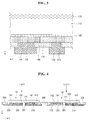
- FIG. 4 illustrates a cross-sectional structure, in which the plurality of solar cells each having above-described configuration are connected in series using the conductive lines 200 and the interconnector 300 as shown in FIG. 1 .
- FIG. 4 is a cross-sectional view taken along line csx1-csx1 of FIG. 1 .
- a plurality of solar cells including a first solar cell C1 and a second solar cell C2 may be arranged in the second direction y.
- a longitudinal direction of a plurality of first and second electrodes 141 and 142 included in the first and second solar cells C1 and C2 may correspond to the first direction x.
- the first and second solar cells C1 and C2, that are arranged in the second direction y as described above, may be connected in series to each other in the second direction y using first and second conductive lines 210 and 220 and an interconnector 300 to form a string.
- the first and second conductive lines 210 and 220 and the interconnector 300 may be formed of a conductive metal material.
- the first and second conductive lines 210 and 220 may be connected to a back surface of a semiconductor substrate 110 of each solar cell and then may be connected to the interconnector 300 for a serial connection of the solar cells.
- Each of the first and second conductive lines 210 and 220 may have a conductive wire shape having a circular cross section or a ribbon shape, in which a linewidth is greater than a thickness.
- the plurality of first conductive lines 210 may overlap the plurality of first electrodes 141 included in each of the first and second solar cells C1 and C2 and may be connected to the plurality of first electrodes 141 through a conductive adhesive 251. Further, the plurality of first conductive lines 210 may be insulated from the plurality of second electrodes 142 included in each of the first and second solar cells C1 and C2 through an insulating layer 252 formed of an insulating material.
- each of the plurality of first conductive lines 210 may protrude to the outside of the semiconductor substrate 110 toward the interconnector 300 disposed between the first and second solar cells C1 and C2.
- the plurality of second conductive lines 220 may overlap the plurality of second electrodes 142 included in each of the first and second solar cells C1 and C2 and may be connected to the plurality of second electrodes 142 through a conductive adhesive 251. Further, the plurality of second conductive lines 220 may be insulated from the plurality of first electrodes 141 included in each of the first and second solar cells C1 and C2 through an insulating layer 252 formed of an insulating material.
- each of the plurality of second conductive lines 220 may protrude to the outside of the semiconductor substrate 110 toward the interconnector 300 disposed between the first and second solar cells C1 and C2.
- the conductive adhesive 251 may be formed of a metal material including tin (Sn) or Sn-containing alloy.
- the conductive adhesive 251 may be formed as one of a solder paste including Sn or Sn-containing alloy, an epoxy solder paste, in which Sn or Sn-containing alloy is included in an epoxy, and a conductive paste.
- the solder paste may include at least one metal material of Sn, SnBi, SnIn, SnAgCu, SnPb, SnBiCuCo, SnBiAg, SnPbAg, or SnAg.
- the epoxy solder paste may be formed by including at least one metal material of Sn, SnBi, SnIn, SnAgCu, SnPb, SnBiCuCo, SnBiAg, SnPbAg, or SnAg in an epoxy resin.
- the conductive adhesive 251 when the conductive adhesive 251 is formed as the conductive paste, the conductive paste may be formed by including at least one metal material of Sn, SnBi, Ag, AgIn, or AgCu in a resin, for example, an epoxy.
- the insulating layer 252 may be made of any material as long as an insulating material is used.
- the insulating layer 252 may use one insulating material of an epoxy-based resin, polyimide, polyethylene, an acrylic-based resin, and a silicone-based resin.
- the conductive adhesive 251 may be positioned only on the back surface of the first electrode or the second electrode positioned in a portion crossing the conductive line 200.
- the insulating layer 252 may be positioned not only on the back surface of the first electrode or the second electrode positioned in a portion crossing the conductive line 200 but also on the back surface of the semiconductor substrate 110 around the back surface of the first electrode or the second electrode.
- a portion protruding to the outside of the semiconductor substrate 110 in each of the first and second conductive lines 210 and 220 connected to the back surface of each solar cell may be commonly connected to the back surface of the interconnector 300 between the first and second solar cells C1 and C2.
- the plurality of solar cells C1 and C2 may be connected in series to each other in the second direction y to form a string.
- the first and second conductive lines 210 and 220 of a solar cell having the bad connection may be disconnected from the interconnector 300. Hence, only the bad solar cell can be easily replaced.
- a first direction length L251 of the conductive adhesive 251 and a first direction length L252 of the insulating layer 252 are described in detail below.
- FIG. 5 illustrates in detail a length of a conductive adhesive in a first direction and a length of an insulating layer in the first direction. More specifically, FIG. 5 illustrates an example of an enlarged view of a portion, in which the conductive lines 200 is attached to the back surface of the semiconductor substrate 110.
- FIG. 5 configuration of FIG. 5 is illustrated using the solar cell module illustrated in FIGS. 1 to 4 as an example. However, the configuration of FIG. 5 may be equally applied to another example of a solar cell module shown in FIG. 6 .
- a first direction length L251 of the conductive adhesive 251 and a first direction length L252 of the insulating layer 252 may be equal to or greater than a linewidth W200 of each conductive line 200 and may be less than a distance D200 between the conductive lines 200.
- the first direction length L251 of the conductive adhesive 251 indicates a maximum length between both ends of the conductive adhesive 251 protruding in the first direction x while overlapping the conductive line 200.
- the first direction length L252 of the insulating layer 252 indicates a maximum length between both ends of the insulating layer 252 protruding in the first direction x while overlapping the conductive line 200.
- the first direction length L251 of the conductive adhesive 251 and the first direction length L252 of the insulating layer 252 may be equal to or greater than the linewidth W200 of the conductive line 200 and may be less than the distance D200 between the conductive lines 200.
- the first direction length L252 of the insulating layer 252 may be greater than the first direction length L251 of the conductive adhesive 251.
- a contact resistance between the conductive line 200 and the plurality of first and second electrodes 141 and 142 can be sufficiently reduced by sufficiently connecting the conductive line 200 to the conductive adhesive 251 during a tabbing process for connecting the conductive line 200 to the back surface of the semiconductor substrate 110.
- the short circuit between the unintended electrode 141 or 142 and the conductive line 200 can be minimized during the tabbing process for connecting the conductive line 200 to the back surface of the semiconductor substrate 110.
- the conductive adhesive 251 may spread to an electrode having a different polarity and adjacent to an electrode to which the conductive adhesive 251 is contacted, and may be connected to the electrode of the different polarity. Hence, a short circuit between the unintended electrode 141 or 142 and the conductive line 200 may be generated.
- the conductive adhesive 251 can be previously prevented from being connected to the adjacent electrode having a different polarity, even if the conductive adhesive 251 spreads in the second direction y during the tabbing process. Hence, a defective possibility of the solar cell module can be minimized.
- the first direction length L252 of the insulating layer 252 may be greater than the linewidth W200 of the conductive line 200 and may be less than the distance D200 between the conductive lines 200.
- a ratio of the linewidth W200 of the conductive line 200 to the first direction length L252 of the insulating layer 252 may be 1: 1.1 to 1: 2.
- the manufacturing cost can be reduced by preventing an excessive use of the insulating layer 252.
- the linewidth W200 of the conductive line 200 may be 1 mm to 2.5 mm, and the distance D200 between the conductive lines 200 may be equal to or greater than 2 mm and may be equal to or less than 0.5 times a length of the semiconductor substrate 110 in the first direction x. More preferably, the distance D200 between the conductive lines 200 may be 4 mm to 8 mm.
- the first direction length L252 of the insulating layer 252 may be equal to or greater than the linewidth W200 of the conductive line 200 and may be less than the distance D200 between the conductive lines 200.
- the first direction length L252 of the insulating layer 252 may be 1.1 mm to 4 mm in consideration of the process margin, the prevention of the short circuit, and the manufacturing cost.
- the first direction length L251 of the conductive adhesive 251 may be equal to or greater than the linewidth W200 of the conductive line 200 and may be less than the first direction length L252 of the insulating layer 252.
- a ratio of the linewidth W200 of the conductive line 200 to the first direction length L251 of the conductive adhesive 251 may be 1: 1 to 1: 1.25.
- the conductive line 200 can be more stably attached to an intended electrode through the conductive adhesive 251, and a contact resistance between the conductive line 200 and the intended electrode can be sufficiently reduced.
- the ratio of the linewidth W200 of the conductive line 200 to the first direction length L251 of the conductive adhesive 251 is equal to or less than 1: 1.25, the manufacturing cost can be reduced by minimizing the use of the conductive adhesive 251.
- the first direction length L251 of the conductive adhesive 251 may be equal to or greater than the linewidth W200 of the conductive line 200 and may be less than the first direction length L252 of the insulating layer 252.
- the first direction length L251 of the conductive adhesive 251 may be 1 mm to 3 mm in consideration of the above-described contact resistance and the manufacturing cost.
- a ratio of the first direction length L251 of the conductive adhesive 251 to the first direction length L252 of the insulating layer 252 may be 1: 1.1 to 1: 1.7.
- the ratio of the first direction length L251 of the conductive adhesive 251 to the first direction length L252 of the insulating layer 252 is equal to or greater than 1: 1.1, a short circuit between an unintended electrode and the conductive line 200 can be prevented.
- the embodiment of the invention can secure a proper process margin during the tabbing process while preventing an excessive use of the insulating layer 252.
- linewidths W141 and W142 of the first and second electrodes 141 and 142 may be less than the first direction length L251 of the conductive adhesive 251 and the first direction length L252 of the insulating layer 252.
- the linewidths W141and W142 of the first and second electrodes 141 and 142 may be 180 ⁇ m to 400 ⁇ m.
- a distance DE between the first and second electrodes 141 and 142 may be less than the first direction length L251 of the conductive adhesive 251 and the first direction length L252 of the insulating layer 252.
- the distance DE between the first and second electrodes 141 and 142 may be 0.5 mm to 1.5 mm.
- a linewidth W251 of the conductive adhesive 251 may be less than the first direction length L251 of the conductive adhesive 251, and a linewidth W252 of the insulating layer 252 may be less than the first direction length L252 of the insulating layer 252.
- the linewidth W252 of the insulating layer 252 may be greater than the linewidth W251 of the conductive adhesive 251 in consideration of the prevention of the short circuit.
- the linewidth W252 of the insulating layer 252 may be 200 ⁇ m to 450 ⁇ m, and the linewidth W251 of the conductive adhesive 251 may be 180 ⁇ m to 400 ⁇ m.
- the linewidth W251 of the conductive adhesive 251 may be substantially equal to the linewidths W141 and W142 of the first and second electrodes 141 and 142.
Landscapes
- Photovoltaic Devices (AREA)
- Life Sciences & Earth Sciences (AREA)
- Engineering & Computer Science (AREA)
- Sustainable Development (AREA)
- Sustainable Energy (AREA)
Applications Claiming Priority (1)
| Application Number | Priority Date | Filing Date | Title |
|---|---|---|---|
| KR1020150125286A KR20170028548A (ko) | 2015-09-04 | 2015-09-04 | 태양 전지 모듈 |
Publications (2)
| Publication Number | Publication Date |
|---|---|
| EP3139414A1 true EP3139414A1 (fr) | 2017-03-08 |
| EP3139414B1 EP3139414B1 (fr) | 2019-12-04 |
Family
ID=56853519
Family Applications (1)
| Application Number | Title | Priority Date | Filing Date |
|---|---|---|---|
| EP16186990.4A Active EP3139414B1 (fr) | 2015-09-04 | 2016-09-02 | Module de cellule solaire |
Country Status (5)
| Country | Link |
|---|---|
| US (1) | US20170069771A1 (fr) |
| EP (1) | EP3139414B1 (fr) |
| JP (1) | JP6321099B2 (fr) |
| KR (1) | KR20170028548A (fr) |
| CN (1) | CN106505122B (fr) |
Families Citing this family (6)
| Publication number | Priority date | Publication date | Assignee | Title |
|---|---|---|---|---|
| JP6741626B2 (ja) * | 2017-06-26 | 2020-08-19 | 信越化学工業株式会社 | 高効率裏面電極型太陽電池及びその製造方法 |
| JPWO2021177356A1 (fr) * | 2020-03-05 | 2021-09-10 | ||
| CN216719958U (zh) * | 2021-08-25 | 2022-06-10 | 泰州隆基乐叶光伏科技有限公司 | 一种太阳能电池片、太阳能电池分片及光伏组件 |
| CN114126262A (zh) * | 2021-11-12 | 2022-03-01 | 深圳市华鼎星科技有限公司 | 双层导电线路及其制作方法及显示模组 |
| CN117542914B (zh) * | 2023-11-23 | 2024-12-03 | 江西沐邦高科股份有限公司 | 太阳能电池组件及其制造方法 |
| CN118472057B (zh) * | 2024-07-11 | 2025-06-03 | 隆基绿能科技股份有限公司 | 一种电池串及光伏组件 |
Citations (3)
| Publication number | Priority date | Publication date | Assignee | Title |
|---|---|---|---|---|
| EP2184787A1 (fr) * | 2007-08-23 | 2010-05-12 | Sharp Kabushiki Kaisha | Cellule solaire du type à connexion par la surface arrière, cellule solaire du type à connexion par la surface arrière ayant une carte de câblage, chaîne de cellules solaires et module de cellule solaire |
| EP2911207A1 (fr) * | 2014-02-24 | 2015-08-26 | LG Electronics Inc. | Module de cellule solaire |
| EP2911206A2 (fr) * | 2014-02-24 | 2015-08-26 | LG Electronics Inc. | Module de cellule solaire et son procédé de fabrication |
Family Cites Families (7)
| Publication number | Priority date | Publication date | Assignee | Title |
|---|---|---|---|---|
| JP3743743B2 (ja) * | 1999-03-09 | 2006-02-08 | 三菱電機株式会社 | 太陽電池 |
| JP5025135B2 (ja) * | 2006-01-24 | 2012-09-12 | 三洋電機株式会社 | 光起電力モジュール |
| JP2011003724A (ja) * | 2009-06-18 | 2011-01-06 | Sanyo Electric Co Ltd | 太陽電池モジュール |
| JP2013033819A (ja) * | 2011-08-01 | 2013-02-14 | Jx Nippon Oil & Energy Corp | 太陽電池モジュール及びその製造方法 |
| JP5889701B2 (ja) * | 2012-04-06 | 2016-03-22 | デクセリアルズ株式会社 | 結晶系太陽電池モジュール及びその製造方法 |
| US9048374B1 (en) * | 2013-11-20 | 2015-06-02 | E I Du Pont De Nemours And Company | Method for manufacturing an interdigitated back contact solar cell |
| KR102257808B1 (ko) * | 2014-01-20 | 2021-05-28 | 엘지전자 주식회사 | 태양 전지 모듈 |
-
2015
- 2015-09-04 KR KR1020150125286A patent/KR20170028548A/ko not_active Ceased
-
2016
- 2016-09-02 JP JP2016171856A patent/JP6321099B2/ja active Active
- 2016-09-02 EP EP16186990.4A patent/EP3139414B1/fr active Active
- 2016-09-02 US US15/256,118 patent/US20170069771A1/en not_active Abandoned
- 2016-09-05 CN CN201610801702.9A patent/CN106505122B/zh active Active
Patent Citations (3)
| Publication number | Priority date | Publication date | Assignee | Title |
|---|---|---|---|---|
| EP2184787A1 (fr) * | 2007-08-23 | 2010-05-12 | Sharp Kabushiki Kaisha | Cellule solaire du type à connexion par la surface arrière, cellule solaire du type à connexion par la surface arrière ayant une carte de câblage, chaîne de cellules solaires et module de cellule solaire |
| EP2911207A1 (fr) * | 2014-02-24 | 2015-08-26 | LG Electronics Inc. | Module de cellule solaire |
| EP2911206A2 (fr) * | 2014-02-24 | 2015-08-26 | LG Electronics Inc. | Module de cellule solaire et son procédé de fabrication |
Also Published As
| Publication number | Publication date |
|---|---|
| US20170069771A1 (en) | 2017-03-09 |
| CN106505122A (zh) | 2017-03-15 |
| KR20170028548A (ko) | 2017-03-14 |
| CN106505122B (zh) | 2020-01-17 |
| JP6321099B2 (ja) | 2018-05-09 |
| EP3139414B1 (fr) | 2019-12-04 |
| JP2017050540A (ja) | 2017-03-09 |
Similar Documents
| Publication | Publication Date | Title |
|---|---|---|
| US11152525B2 (en) | Solar cell module | |
| EP3116034B1 (fr) | Module de cellule solaire | |
| EP3139414B1 (fr) | Module de cellule solaire | |
| US10276737B2 (en) | Solar cell and solar cell module | |
| EP3144981B1 (fr) | Module de cellule solaire | |
| EP2757595B1 (fr) | Cellule solaire et son procédé de fabrication | |
| KR101642231B1 (ko) | 태양 전지 모듈 | |
| US10714642B2 (en) | Solar cell and solar cell module | |
| KR101975586B1 (ko) | 태양 전지 모듈 | |
| KR101911844B1 (ko) | 태양 전지 모듈 | |
| KR20170028907A (ko) | 태양 전지 모듈 | |
| KR101656622B1 (ko) | 태양 전지 모듈 및 그 제조 방법 | |
| KR102183580B1 (ko) | 태양 전지 및 태양 전지 모듈 | |
| KR101788170B1 (ko) | 태양 전지 및 태양 전지 모듈 | |
| KR20170009805A (ko) | 태양 전지 및 태양 전지 모듈 | |
| KR20160063130A (ko) | 태양 전지 및 태양 전지 모듈 | |
| KR20160136562A (ko) | 태양 전지 |
Legal Events
| Date | Code | Title | Description |
|---|---|---|---|
| PUAI | Public reference made under article 153(3) epc to a published international application that has entered the european phase |
Free format text: ORIGINAL CODE: 0009012 |
|
| STAA | Information on the status of an ep patent application or granted ep patent |
Free format text: STATUS: THE APPLICATION HAS BEEN PUBLISHED |
|
| AK | Designated contracting states |
Kind code of ref document: A1 Designated state(s): AL AT BE BG CH CY CZ DE DK EE ES FI FR GB GR HR HU IE IS IT LI LT LU LV MC MK MT NL NO PL PT RO RS SE SI SK SM TR |
|
| AX | Request for extension of the european patent |
Extension state: BA ME |
|
| STAA | Information on the status of an ep patent application or granted ep patent |
Free format text: STATUS: REQUEST FOR EXAMINATION WAS MADE |
|
| 17P | Request for examination filed |
Effective date: 20170817 |
|
| RBV | Designated contracting states (corrected) |
Designated state(s): AL AT BE BG CH CY CZ DE DK EE ES FI FR GB GR HR HU IE IS IT LI LT LU LV MC MK MT NL NO PL PT RO RS SE SI SK SM TR |
|
| STAA | Information on the status of an ep patent application or granted ep patent |
Free format text: STATUS: EXAMINATION IS IN PROGRESS |
|
| 17Q | First examination report despatched |
Effective date: 20180424 |
|
| GRAP | Despatch of communication of intention to grant a patent |
Free format text: ORIGINAL CODE: EPIDOSNIGR1 |
|
| STAA | Information on the status of an ep patent application or granted ep patent |
Free format text: STATUS: GRANT OF PATENT IS INTENDED |
|
| INTG | Intention to grant announced |
Effective date: 20190704 |
|
| RIN1 | Information on inventor provided before grant (corrected) |
Inventor name: JANG, DAEHEE Inventor name: HYUN, DAESEON Inventor name: KIM, BOJOONG |
|
| GRAS | Grant fee paid |
Free format text: ORIGINAL CODE: EPIDOSNIGR3 |
|
| GRAA | (expected) grant |
Free format text: ORIGINAL CODE: 0009210 |
|
| STAA | Information on the status of an ep patent application or granted ep patent |
Free format text: STATUS: THE PATENT HAS BEEN GRANTED |
|
| AK | Designated contracting states |
Kind code of ref document: B1 Designated state(s): AL AT BE BG CH CY CZ DE DK EE ES FI FR GB GR HR HU IE IS IT LI LT LU LV MC MK MT NL NO PL PT RO RS SE SI SK SM TR |
|
| REG | Reference to a national code |
Ref country code: GB Ref legal event code: FG4D |
|
| REG | Reference to a national code |
Ref country code: CH Ref legal event code: EP |
|
| REG | Reference to a national code |
Ref country code: AT Ref legal event code: REF Ref document number: 1210493 Country of ref document: AT Kind code of ref document: T Effective date: 20191215 |
|
| REG | Reference to a national code |
Ref country code: DE Ref legal event code: R096 Ref document number: 602016025401 Country of ref document: DE |
|
| REG | Reference to a national code |
Ref country code: IE Ref legal event code: FG4D |
|
| REG | Reference to a national code |
Ref country code: NL Ref legal event code: MP Effective date: 20191204 |
|
| REG | Reference to a national code |
Ref country code: LT Ref legal event code: MG4D |
|
| PG25 | Lapsed in a contracting state [announced via postgrant information from national office to epo] |
Ref country code: NO Free format text: LAPSE BECAUSE OF FAILURE TO SUBMIT A TRANSLATION OF THE DESCRIPTION OR TO PAY THE FEE WITHIN THE PRESCRIBED TIME-LIMIT Effective date: 20200304 Ref country code: BG Free format text: LAPSE BECAUSE OF FAILURE TO SUBMIT A TRANSLATION OF THE DESCRIPTION OR TO PAY THE FEE WITHIN THE PRESCRIBED TIME-LIMIT Effective date: 20200304 Ref country code: FI Free format text: LAPSE BECAUSE OF FAILURE TO SUBMIT A TRANSLATION OF THE DESCRIPTION OR TO PAY THE FEE WITHIN THE PRESCRIBED TIME-LIMIT Effective date: 20191204 Ref country code: LT Free format text: LAPSE BECAUSE OF FAILURE TO SUBMIT A TRANSLATION OF THE DESCRIPTION OR TO PAY THE FEE WITHIN THE PRESCRIBED TIME-LIMIT Effective date: 20191204 Ref country code: GR Free format text: LAPSE BECAUSE OF FAILURE TO SUBMIT A TRANSLATION OF THE DESCRIPTION OR TO PAY THE FEE WITHIN THE PRESCRIBED TIME-LIMIT Effective date: 20200305 Ref country code: SE Free format text: LAPSE BECAUSE OF FAILURE TO SUBMIT A TRANSLATION OF THE DESCRIPTION OR TO PAY THE FEE WITHIN THE PRESCRIBED TIME-LIMIT Effective date: 20191204 Ref country code: LV Free format text: LAPSE BECAUSE OF FAILURE TO SUBMIT A TRANSLATION OF THE DESCRIPTION OR TO PAY THE FEE WITHIN THE PRESCRIBED TIME-LIMIT Effective date: 20191204 |
|
| PG25 | Lapsed in a contracting state [announced via postgrant information from national office to epo] |
Ref country code: RS Free format text: LAPSE BECAUSE OF FAILURE TO SUBMIT A TRANSLATION OF THE DESCRIPTION OR TO PAY THE FEE WITHIN THE PRESCRIBED TIME-LIMIT Effective date: 20191204 Ref country code: HR Free format text: LAPSE BECAUSE OF FAILURE TO SUBMIT A TRANSLATION OF THE DESCRIPTION OR TO PAY THE FEE WITHIN THE PRESCRIBED TIME-LIMIT Effective date: 20191204 |
|
| PG25 | Lapsed in a contracting state [announced via postgrant information from national office to epo] |
Ref country code: AL Free format text: LAPSE BECAUSE OF FAILURE TO SUBMIT A TRANSLATION OF THE DESCRIPTION OR TO PAY THE FEE WITHIN THE PRESCRIBED TIME-LIMIT Effective date: 20191204 |
|
| PG25 | Lapsed in a contracting state [announced via postgrant information from national office to epo] |
Ref country code: PT Free format text: LAPSE BECAUSE OF FAILURE TO SUBMIT A TRANSLATION OF THE DESCRIPTION OR TO PAY THE FEE WITHIN THE PRESCRIBED TIME-LIMIT Effective date: 20200429 Ref country code: EE Free format text: LAPSE BECAUSE OF FAILURE TO SUBMIT A TRANSLATION OF THE DESCRIPTION OR TO PAY THE FEE WITHIN THE PRESCRIBED TIME-LIMIT Effective date: 20191204 Ref country code: CZ Free format text: LAPSE BECAUSE OF FAILURE TO SUBMIT A TRANSLATION OF THE DESCRIPTION OR TO PAY THE FEE WITHIN THE PRESCRIBED TIME-LIMIT Effective date: 20191204 Ref country code: RO Free format text: LAPSE BECAUSE OF FAILURE TO SUBMIT A TRANSLATION OF THE DESCRIPTION OR TO PAY THE FEE WITHIN THE PRESCRIBED TIME-LIMIT Effective date: 20191204 Ref country code: NL Free format text: LAPSE BECAUSE OF FAILURE TO SUBMIT A TRANSLATION OF THE DESCRIPTION OR TO PAY THE FEE WITHIN THE PRESCRIBED TIME-LIMIT Effective date: 20191204 Ref country code: ES Free format text: LAPSE BECAUSE OF FAILURE TO SUBMIT A TRANSLATION OF THE DESCRIPTION OR TO PAY THE FEE WITHIN THE PRESCRIBED TIME-LIMIT Effective date: 20191204 |
|
| PG25 | Lapsed in a contracting state [announced via postgrant information from national office to epo] |
Ref country code: SM Free format text: LAPSE BECAUSE OF FAILURE TO SUBMIT A TRANSLATION OF THE DESCRIPTION OR TO PAY THE FEE WITHIN THE PRESCRIBED TIME-LIMIT Effective date: 20191204 Ref country code: SK Free format text: LAPSE BECAUSE OF FAILURE TO SUBMIT A TRANSLATION OF THE DESCRIPTION OR TO PAY THE FEE WITHIN THE PRESCRIBED TIME-LIMIT Effective date: 20191204 Ref country code: IS Free format text: LAPSE BECAUSE OF FAILURE TO SUBMIT A TRANSLATION OF THE DESCRIPTION OR TO PAY THE FEE WITHIN THE PRESCRIBED TIME-LIMIT Effective date: 20200404 |
|
| REG | Reference to a national code |
Ref country code: DE Ref legal event code: R097 Ref document number: 602016025401 Country of ref document: DE |
|
| REG | Reference to a national code |
Ref country code: AT Ref legal event code: MK05 Ref document number: 1210493 Country of ref document: AT Kind code of ref document: T Effective date: 20191204 |
|
| PLBE | No opposition filed within time limit |
Free format text: ORIGINAL CODE: 0009261 |
|
| STAA | Information on the status of an ep patent application or granted ep patent |
Free format text: STATUS: NO OPPOSITION FILED WITHIN TIME LIMIT |
|
| PG25 | Lapsed in a contracting state [announced via postgrant information from national office to epo] |
Ref country code: DK Free format text: LAPSE BECAUSE OF FAILURE TO SUBMIT A TRANSLATION OF THE DESCRIPTION OR TO PAY THE FEE WITHIN THE PRESCRIBED TIME-LIMIT Effective date: 20191204 |
|
| 26N | No opposition filed |
Effective date: 20200907 |
|
| PG25 | Lapsed in a contracting state [announced via postgrant information from national office to epo] |
Ref country code: PL Free format text: LAPSE BECAUSE OF FAILURE TO SUBMIT A TRANSLATION OF THE DESCRIPTION OR TO PAY THE FEE WITHIN THE PRESCRIBED TIME-LIMIT Effective date: 20191204 Ref country code: SI Free format text: LAPSE BECAUSE OF FAILURE TO SUBMIT A TRANSLATION OF THE DESCRIPTION OR TO PAY THE FEE WITHIN THE PRESCRIBED TIME-LIMIT Effective date: 20191204 Ref country code: AT Free format text: LAPSE BECAUSE OF FAILURE TO SUBMIT A TRANSLATION OF THE DESCRIPTION OR TO PAY THE FEE WITHIN THE PRESCRIBED TIME-LIMIT Effective date: 20191204 |
|
| PG25 | Lapsed in a contracting state [announced via postgrant information from national office to epo] |
Ref country code: IT Free format text: LAPSE BECAUSE OF FAILURE TO SUBMIT A TRANSLATION OF THE DESCRIPTION OR TO PAY THE FEE WITHIN THE PRESCRIBED TIME-LIMIT Effective date: 20191204 |
|
| PG25 | Lapsed in a contracting state [announced via postgrant information from national office to epo] |
Ref country code: MC Free format text: LAPSE BECAUSE OF FAILURE TO SUBMIT A TRANSLATION OF THE DESCRIPTION OR TO PAY THE FEE WITHIN THE PRESCRIBED TIME-LIMIT Effective date: 20191204 |
|
| REG | Reference to a national code |
Ref country code: CH Ref legal event code: PL |
|
| GBPC | Gb: european patent ceased through non-payment of renewal fee |
Effective date: 20200902 |
|
| REG | Reference to a national code |
Ref country code: BE Ref legal event code: MM Effective date: 20200930 |
|
| PG25 | Lapsed in a contracting state [announced via postgrant information from national office to epo] |
Ref country code: LU Free format text: LAPSE BECAUSE OF NON-PAYMENT OF DUE FEES Effective date: 20200902 |
|
| PG25 | Lapsed in a contracting state [announced via postgrant information from national office to epo] |
Ref country code: FR Free format text: LAPSE BECAUSE OF NON-PAYMENT OF DUE FEES Effective date: 20200930 |
|
| PG25 | Lapsed in a contracting state [announced via postgrant information from national office to epo] |
Ref country code: CH Free format text: LAPSE BECAUSE OF NON-PAYMENT OF DUE FEES Effective date: 20200930 Ref country code: BE Free format text: LAPSE BECAUSE OF NON-PAYMENT OF DUE FEES Effective date: 20200930 Ref country code: GB Free format text: LAPSE BECAUSE OF NON-PAYMENT OF DUE FEES Effective date: 20200902 Ref country code: IE Free format text: LAPSE BECAUSE OF NON-PAYMENT OF DUE FEES Effective date: 20200902 Ref country code: LI Free format text: LAPSE BECAUSE OF NON-PAYMENT OF DUE FEES Effective date: 20200930 |
|
| PG25 | Lapsed in a contracting state [announced via postgrant information from national office to epo] |
Ref country code: TR Free format text: LAPSE BECAUSE OF FAILURE TO SUBMIT A TRANSLATION OF THE DESCRIPTION OR TO PAY THE FEE WITHIN THE PRESCRIBED TIME-LIMIT Effective date: 20191204 Ref country code: MT Free format text: LAPSE BECAUSE OF FAILURE TO SUBMIT A TRANSLATION OF THE DESCRIPTION OR TO PAY THE FEE WITHIN THE PRESCRIBED TIME-LIMIT Effective date: 20191204 Ref country code: CY Free format text: LAPSE BECAUSE OF FAILURE TO SUBMIT A TRANSLATION OF THE DESCRIPTION OR TO PAY THE FEE WITHIN THE PRESCRIBED TIME-LIMIT Effective date: 20191204 |
|
| PG25 | Lapsed in a contracting state [announced via postgrant information from national office to epo] |
Ref country code: MK Free format text: LAPSE BECAUSE OF FAILURE TO SUBMIT A TRANSLATION OF THE DESCRIPTION OR TO PAY THE FEE WITHIN THE PRESCRIBED TIME-LIMIT Effective date: 20191204 |
|
| REG | Reference to a national code |
Ref country code: DE Ref legal event code: R081 Ref document number: 602016025401 Country of ref document: DE Owner name: SHANGRAO JINKO SOLAR TECHNOLOGY DEVELOPMENT CO, CN Free format text: FORMER OWNER: LG ELECTRONICS INC., SEOUL, KR Ref country code: DE Ref legal event code: R082 Ref document number: 602016025401 Country of ref document: DE Representative=s name: DREISS PATENTANWAELTE PARTG MBB, DE Ref country code: DE Ref legal event code: R082 Ref document number: 602016025401 Country of ref document: DE Representative=s name: MANITZ FINSTERWALD PATENT- UND RECHTSANWALTSPA, DE Ref country code: DE Ref legal event code: R081 Ref document number: 602016025401 Country of ref document: DE Owner name: TRINA SOLAR CO., LTD., CHANGZHOU, CN Free format text: FORMER OWNER: LG ELECTRONICS INC., SEOUL, KR Ref country code: DE Ref legal event code: R081 Ref document number: 602016025401 Country of ref document: DE Owner name: SHANGRAO XINYUAN YUEDONG TECHNOLOGY DEVELOPMEN, CN Free format text: FORMER OWNER: LG ELECTRONICS INC., SEOUL, KR |
|
| REG | Reference to a national code |
Ref country code: DE Ref legal event code: R081 Ref document number: 602016025401 Country of ref document: DE Owner name: TRINA SOLAR CO., LTD., CHANGZHOU, CN Free format text: FORMER OWNER: SHANGRAO JINKO SOLAR TECHNOLOGY DEVELOPMENT CO., LTD, SHANGRAO, JIANGXI PROVINCE, CN Ref country code: DE Ref legal event code: R081 Ref document number: 602016025401 Country of ref document: DE Owner name: SHANGRAO XINYUAN YUEDONG TECHNOLOGY DEVELOPMEN, CN Free format text: FORMER OWNER: SHANGRAO JINKO SOLAR TECHNOLOGY DEVELOPMENT CO., LTD, SHANGRAO, JIANGXI PROVINCE, CN |
|
| REG | Reference to a national code |
Ref country code: DE Ref legal event code: R082 Ref document number: 602016025401 Country of ref document: DE Representative=s name: MANITZ FINSTERWALD PATENT- UND RECHTSANWALTSPA, DE Ref country code: DE Ref legal event code: R081 Ref document number: 602016025401 Country of ref document: DE Owner name: TRINA SOLAR CO., LTD., CHANGZHOU, CN Free format text: FORMER OWNER: SHANGRAO XINYUAN YUEDONG TECHNOLOGY DEVELOPMENT CO. LTD, SHANGRAO, JIANGXI PROVINCE, CN |
|
| REG | Reference to a national code |
Ref country code: DE Ref legal event code: R079 Ref document number: 602016025401 Country of ref document: DE Free format text: PREVIOUS MAIN CLASS: H01L0031022400 Ipc: H10F0077200000 |
|
| PGFP | Annual fee paid to national office [announced via postgrant information from national office to epo] |
Ref country code: DE Payment date: 20250919 Year of fee payment: 10 |