EP3140910B1 - Analog-digital-slope-wandler zur direkten bereitstellung von durchschnittlich zwei signalen - Google Patents
Analog-digital-slope-wandler zur direkten bereitstellung von durchschnittlich zwei signalen Download PDFInfo
- Publication number
- EP3140910B1 EP3140910B1 EP15723174.7A EP15723174A EP3140910B1 EP 3140910 B1 EP3140910 B1 EP 3140910B1 EP 15723174 A EP15723174 A EP 15723174A EP 3140910 B1 EP3140910 B1 EP 3140910B1
- Authority
- EP
- European Patent Office
- Prior art keywords
- ramp
- voltage
- comparator
- counter
- samples
- Prior art date
- Legal status (The legal status is an assumption and is not a legal conclusion. Google has not performed a legal analysis and makes no representation as to the accuracy of the status listed.)
- Active
Links
Images


Classifications
-
- H—ELECTRICITY
- H03—ELECTRONIC CIRCUITRY
- H03M—CODING; DECODING; CODE CONVERSION IN GENERAL
- H03M1/00—Analogue/digital conversion; Digital/analogue conversion
- H03M1/12—Analogue/digital converters
- H03M1/50—Analogue/digital converters with intermediate conversion to time interval
- H03M1/56—Input signal compared with linear ramp
-
- H—ELECTRICITY
- H03—ELECTRONIC CIRCUITRY
- H03M—CODING; DECODING; CODE CONVERSION IN GENERAL
- H03M1/00—Analogue/digital conversion; Digital/analogue conversion
- H03M1/06—Continuously compensating for, or preventing, undesired influence of physical parameters
- H03M1/0617—Continuously compensating for, or preventing, undesired influence of physical parameters characterised by the use of methods or means not specific to a particular type of detrimental influence
- H03M1/0634—Continuously compensating for, or preventing, undesired influence of physical parameters characterised by the use of methods or means not specific to a particular type of detrimental influence by averaging out the errors, e.g. using sliding scale
-
- H—ELECTRICITY
- H03—ELECTRONIC CIRCUITRY
- H03M—CODING; DECODING; CODE CONVERSION IN GENERAL
- H03M1/00—Analogue/digital conversion; Digital/analogue conversion
- H03M1/12—Analogue/digital converters
- H03M1/124—Sampling or signal conditioning arrangements specially adapted for A/D converters
- H03M1/1245—Details of sampling arrangements or methods
-
- H—ELECTRICITY
- H04—ELECTRIC COMMUNICATION TECHNIQUE
- H04N—PICTORIAL COMMUNICATION, e.g. TELEVISION
- H04N25/00—Circuitry of solid-state image sensors [SSIS]; Control thereof
- H04N25/60—Noise processing, e.g. detecting, correcting, reducing or removing noise
- H04N25/616—Noise processing, e.g. detecting, correcting, reducing or removing noise involving a correlated sampling function, e.g. correlated double sampling [CDS] or triple sampling
-
- H—ELECTRICITY
- H03—ELECTRONIC CIRCUITRY
- H03M—CODING; DECODING; CODE CONVERSION IN GENERAL
- H03M1/00—Analogue/digital conversion; Digital/analogue conversion
-
- H—ELECTRICITY
- H03—ELECTRONIC CIRCUITRY
- H03M—CODING; DECODING; CODE CONVERSION IN GENERAL
- H03M1/00—Analogue/digital conversion; Digital/analogue conversion
- H03M1/12—Analogue/digital converters
-
- H—ELECTRICITY
- H03—ELECTRONIC CIRCUITRY
- H03M—CODING; DECODING; CODE CONVERSION IN GENERAL
- H03M1/00—Analogue/digital conversion; Digital/analogue conversion
- H03M1/12—Analogue/digital converters
- H03M1/1205—Multiplexed conversion systems
- H03M1/122—Shared using a single converter or a part thereof for multiple channels, e.g. a residue amplifier for multiple stages
- H03M1/1225—Shared using a single converter or a part thereof for multiple channels, e.g. a residue amplifier for multiple stages using time-division multiplexing
-
- H—ELECTRICITY
- H03—ELECTRONIC CIRCUITRY
- H03M—CODING; DECODING; CODE CONVERSION IN GENERAL
- H03M1/00—Analogue/digital conversion; Digital/analogue conversion
- H03M1/12—Analogue/digital converters
- H03M1/1205—Multiplexed conversion systems
- H03M1/123—Simultaneous, i.e. using one converter per channel but with common control or reference circuits for multiple converters
Definitions
- the invention relates to analog-to-digital ramp converters, especially but not exclusively used in matrix image sensors for providing a digital value representative of a one-pixel illumination level.
- the content of the meter is a digital representation of the difference between the useful voltage and the reference voltage.
- the reference voltage may be a voltage sampled on a column conductor after a reset operation of a pixel, and the useful voltage is the voltage sampled on that same column driver in a read operation. charges generated in the pixel by illumination.
- the solution is to do two analog-to-digital conversions (simultaneous or not) and to digitally add the results of the two conversions.
- this solution requires a processing of numerical values which is cumbersome and cumbersome in an integrated circuit, for example when it is necessary to perform this processing on hundreds of columns of a matrix.
- the documents US2009 / 0309991 A1 , US2009 / 0066554 A1 and US2009 / 0021411 A1 are examples of solutions known in the state of the art.
- the content of the counter then represents a digital average of two analog voltage differences which are the difference between the first two voltage samples applied to the first comparator and the two other voltage samples applied to the second comparator.
- an analog-digital ramp converter which comprises a circuit establishing a voltage ramp, a counter incremented by a clock signal at a frequency F from a start time of the ramp, a comparator for comparing two voltage samples, one of which is added to the ramp, characterized in that the converter comprises a second comparator for comparing two other voltage samples, one of which is added to one ramp identical to the first ramp, a counter counting frequency selection logic circuit, controlled by the comparators, to select the frequency F at the beginning of the ramp and select a frequency half F / 2 when the switchover of one of the comparators , and means for storing the contents of the counter at the time of switching of the other comparator.
- the two comparators receive samples of the same difference of voltages to be converted, that is to say a first pair of samples of the voltages whose difference must be converted and a second pair of samples of these tensions. Conversion noise is reduced by obtaining an average of two conversions without this average requiring two conversions followed by a numerical addition.
- Samples of the same voltage difference to be converted may be samples taken at the same time or samples taken at two different times, preferably at two very close times.
- the two comparators receive simultaneous samples of two different (but neighboring) voltage differences and the converter provides a value which is the average of these two differences.
- the voltage differences to be converted are provided by column conductors (connecting the pixels of the same column) successively providing a potential representing a reset level of the pixel (resetting a photodiode or charge storage node) and a potential representing the illumination of a pixel.
- the voltage differences applied to the two comparators then come either from the same column conductor (to reduce the influence of measurement noise) with a double sampling done at four different times on the column conductor or two column conductors (preferably immediately adjacent), with simultaneous samplings for both columns, to provide a measure of the average illumination received by two pixels.
- the converter converts voltage samples, it being understood that one of the voltage samples may be either a fixed voltage given by a reference source without the need for a sampler, ie a variable voltage sample provided by a sample-and-hold device.
- the content of the counter then represents a digital average of N analog voltage differences which are the voltage differences between the pairs of voltage samples applied to the N comparators.
- the analog-digital converter comprises in this case a circuit establishing a voltage ramp, a counter incremented by a clock signal at a frequency F from a start time of the ramp, a comparator for comparing two voltage samples, one of which is added to the ramp, characterized in that the converter comprises N-1 other comparators for comparing N-1 other voltage samples, one of which is added to a ramp identical to the first ramp, a counting frequency selection logic circuit of the counter, controlled by the comparators, to select the frequency F at the beginning of the ramp and successively select lower frequencies as the comparators switch over, the selected frequency being F (Nj) / N when comparators have toggled. , and means for storing the contents of the counter when the last comparator is switched over.
- FIG. 1 the general structure of a ramp analog-to-digital converter is shown which converts the difference between a variable voltage and a reference voltage into a digital value.
- a two-input COMP comparator E1, E2 receives on these inputs the variable voltage Vin and the reference voltage Vref; an increasing or decreasing linear voltage ramp is added to one of these two voltages from an instant t0 which defines the beginning of the analog-digital conversion.
- the choice of the direction of the ramp or the choice of the input to which the ramp is applied is chosen according to the sign of the difference between the variable voltage and the reference voltage, so that the voltages applied to the two inputs of the comparator become equal after a variable time that defines the end of the conversion.
- the reference voltage is lower than the variable voltage and if the voltage ramp is increasing, it is ensured that the voltages become equal if an increasing ramp is added to the reference voltage or a decreasing ramp to the variable voltage.
- the reference voltage is higher than the variable voltage, it is necessary to apply a decreasing voltage ramp to the reference voltage, or to add an increasing ramp to the variable voltage.
- a counter CNT counts pulses applied to an incrementing input which receives these pulses at a clock frequency F.
- the counting is authorized by an authorization signal EN applied to an authorization input of the counter. This signal starts at time t0 which defines the start of the voltage ramp.
- the output of the comparator switches when the voltage on the input E1 reaches the value Vref due to the growth of the linear ramp.
- the switchover of the comparator then triggers the storage of the contents of the counter, either by stopping the counting or by letting the counter continue but by triggering the storage in a digital memory MEM of the contents of the counter at the instant of switching.
- the counter or the memory then contains a value representative of the time (number of frequency clock periods F) set to equalize the voltages on the two inputs of the comparator, therefore representative of the difference Vref-Vin since the ramp is linear.
- the pixels of a sensor line are read line by line.
- the reading of a line is done in parallel for the P pixels, using as many analog-digital converters as there are pixels in the line.
- Each pixel of rank i of a line being read produces a voltage which is a function of the illumination it has received during an integration period. This voltage is applied to a respective column conductor COL i of rank i.
- the column conductors of the matrix are each connected to the input of a respective analog-to-digital converter.
- the column conductor is connected to the first input of the comparator of the respective converter, and that a decreasing ramp starting at a reference voltage Vref is applied to the other input.
- Vref it will most often be preferred to apply to the input of the comparator a voltage sample taken from the column conductor and blocked during the time of the conversion.
- the reference voltage Vref is a sample of voltage taken and blocked rather than a fixed voltage.
- the figure 3 shows in more detail an example of a converter in the context of an image sensor providing a numerical value after each charge integration phase in a pixel.
- the COL column driver is connected to a dual sampling circuit that takes two voltage samples from that conductor.
- the first sample Vr is a reset voltage of the pixel. This sample is applied to a sampling capacity Cr by closing a switch Kr at a time when the column conductor receives from the pixel a reset level representing a lack of illumination of the pixel. This level is provided by a photodiode or temporary charge storage node of the pixel after this photodiode or node has been brought to a fixed reset potential.
- the second voltage sample Vs is a useful voltage level representing the illumination of the pixel. It is applied to another capacitor Cs by closing a switch Ks at a moment when the column conductor receives from the pixel a voltage representing its illumination. This level is provided by the photodiode after an integration time, or by the temporary storage node of charges after the charges of a photodiode have been transferred to this node.
- the voltage samples Vr and Vs are blocked and maintained in the capacitors Cr and Cs by the opening of the respective switches Kr and Ks.
- the capacitance Cr is connected between the input E2 of the comparator COMP and a ground with zero potential.
- the capacitor Cs is connected between the input E1 of the comparator and the output of a linear voltage ramp generator.
- the generator produces a ramp V RMP from the load of a capacity C RMP by a constant current source I RMP .
- the capacity C RMP is for example connected to the ground.
- the generator output is taken at the junction point of the C RMP capacitance and the current source.
- the capacity C RMP can be short-circuited by a switch K RMP . The opening of this switch under the action of an authorization signal EN at a time t 0 allows the charging of the capacitor C RMP and linearly raises the potential of the input E1 of the comparator from the voltage which was sampled in the Cs capacity.
- the counter receives a clk clock signal at frequency F.
- the count is triggered by the same authorization signal EN which serves to control the opening of the switch K RMP , that is to say by the signal which triggers the start of analog-to-digital conversion by starting the ramp.
- the output of the comparator COMP switches when the voltage VS + V RMP on the input E1 reaches the value of the reference voltage Vr on the input E2.
- the switch triggers the storage of the contents of the counter in the memory MEM.
- the memory can be split to speed up the operation of the sensor: each converter has two memories, one of which can be used for reading while the other is used in writing and vice versa; the switchover of the comparator triggers the memorization at each new conversion alternately in one of the memories then in the other. This constitution with two memories is not related to the present invention and will not be described in more detail.
- the figure 4 represents the timing diagram of a read and analog-to-digital conversion sequence for a pixel of a matrix image sensor.
- the voltage is a voltage Vr representing a reset level of the pixel or a useful voltage Vs representing the illumination according to the moment when one is placed. It will be assumed here that the reset level and the useful level are read on a temporary charge storage node of the pixel, connected via a read transistor of the pixel to the column conductor when selecting the line.
- the reset level Vr is read before the useful level Vs: the pixel is reinitialized then a short closing control signal SHR is applied to the switch Kr to sample the resetting voltage level in the capacitor Cr. Vr. This level Vr is kept throughout the conversion phase after reopening of the switch Kr and it is applied to the input E2 of the comparator COMP.
- the state of the comparator output is represented on the line COMP; by convention, it is considered that it is a low state at the instant t 0 of the beginning of the ramp.
- the counter is also triggered by the counter CNT; the count is incremented at the rate given by a clock at frequency F.
- Arbitrary numbers are indicated on the figure 4 to represent the content of the counter: CNT line.
- the comparator is restored to its initial state at the beginning of a next reading and conversion sequence or it naturally returns to it at the time of sampling of the reset level by the signal SHR.
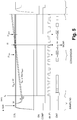
- the figure 5 represents the same chronogram as the figure 4 but the level of voltage to be converted is noisy, both with respect to the reset level Vr and the useful level Vs.
- This noise has been represented as curves parallel to the levels of the figure 4 but on both sides of these.
- the level Vr can vary within a certain range of values because of the noise, and the level Vs also, in a manner independent of the level Vr. This means that we are not sure of the exact moment of crossing of the voltages on the inputs E1 and E2 of the comparator when the input receives the voltage VS + V RMP increasing linearly.
- the moment of the crossing can vary between two limit times t1 MIN and t1 MAX .
- a crossing at time t1 MIN occurs in the extreme configuration where Vr is at a real low level considering the noise while Vs is at a higher level given the noise.
- a crossing at time t1 MAX occurs in the extreme configuration where Vr is at a real level at the highest given the noise while Vs is at a low level given the noise.
- the switchover of the comparator can therefore intervene as we see on the figure 5 at times for which the content of the counter is not the theoretical content it should contain.
- the theoretical content of the counter at the moment of switching is 559, but it is 556 at time t1 MIN and 562 at time t1 MAX .
- the noise can come from phenomena upstream of the converter, but also the offset of the comparator and other sources of noise inside the converter.
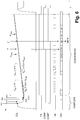
- the invention proposes a method which will be understood by reference to the figure 6 for the timeline and at the figure 7 for the constitution of the conversion circuit.
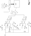
- This method consists in using two samplers which each take a pair of samples of the same measurement, and two comparators COMP and COMP ', but a single counter CNT to count a value which represents the average of the two sample differences, without having need to convert each pair of samples to add them numerically.
- pair of samples is meant here the sample Vr and the sample Vs.
- the four samples can be taken at four different times. We consider here that they are taken at four different moments.
- the two samplers are identical to that of the figure 3 and their operation will not be described again. They comprise capacitors Cr, Cs and C'r, C's respectively, switches Kr, Ks and K'r, K's respectively. Samples for Vr are taken at two moments close defined by sampling commands SHR and SHR 'and are called Vr1 and V'r1, and the same for the samples of Vs, taken at times SHS and SHS' and called Vs1 and V's1. The same linear ramp V RMP is applied to the capacities Cs and C's (or in any case two identical ramps starting at the same instant). The circuit elements are identical in constitution and numerical values in the two samplers. The authorization signal EN is common. The voltages applied to the inputs of the first comparator are V E1 and V E2 . Those applied to the second comparator are V ' E1 and V' E2 .
- the crossing of the curves V E1 and V E2 on the figure 5 would give a moment of tilting of the first comparator at an intermediate instant t1 between t1 MIN and t1 MAX .
- the crossing of the curves V E1 and V E'2 for the second comparator gives a switchover of the second comparator at a time t'1, also intermediate between t1 MIN and t1 MAX .
- the time t1 may be before or after the instant t'1 depending on whether it is the first comparator or the second comparator that switches first.
- the counting frequency of the counter is halved. So we count more slowly.
- the contents of the counter are read, that is to say that the content of the counter is stored in the memory MEM.
- This content is an average of the two samplings and this average is directly recorded in the memory, without there being need to obtain a numerical value for the first sample and a numerical value for the second. This average reduces the measurement uncertainty in the presence of noise.
- the result of the conversion could go from 556 to 562 for a theoretical value of 559 if the signal was not noisy.
- the result of the conversion given by the switching of the comparator which switches to second, is 559 because of the counting frequency F / 2.
- the tilting of the first comparator in the presence of samples Vr1 and Vs1 gives a result 558. If the counting was continued at frequency F as at figure 5 the tilting of the second comparator in the presence of the samples V'r1 and V's1 would have given a result 560.
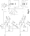
- the figure 7 represents the corresponding diagram of the conversion circuit.
- the signal to be converted is again supposed to be a signal coming from a column driver COL of a matrix image sensor, on which a reset level then successively appears and a level that is useful for a differential measurement.
- the outputs of comparators COMP and COMP ' are connected to a small logic circuit (an AND gate 10 and an OR gate 12) which determines which comparator switches first and which controls the storage of the contents of the counter in the memory from the switchover of the other comparator.
- the outputs of the comparators are considered to be active at the high logical level after switching. They are connected to the two inputs of the OR gate 10.
- the output of the OR gate activates a switch SW which points to the counter incrementation control input either a frequency clock F (gate output OR low) either an F / 2 clock (gate output OR high). Initially, the counting frequency is F. It becomes F / 2 as soon as one of the comparators switches over.
- the outputs of the comparators are connected to the inputs of the AND gate.
- the output of the AND gate remains low until both comparators have toggled. When it goes high, it controls the storage of the contents of the counter in the memory.
- N can range from 3 to 10.
- N comparators are used and not not two.
- Each comparator of rank i receives a respective pair of samples of rank i, V i r, V i s, among N couples for which we want to obtain directly a numerical value of the mean of the differences V i rV i s.
- the outputs of the comparators are connected to the inputs of a logic circuit more complex than that of the figure 7 that is to say, more complex than a simple pair of AND and OR gates.
- This circuit has the logical function of determining the number j of comparators which have switched at a given instant and consequently of controlling a selection circuit of a frequency among N possible frequencies which are the frequencies F, (N-1) F / NOT, (N-2) F / N, etc ... F / N.
- the logic circuit selects the frequency F at the start of the conversion, that is to say at the start of the linear ramp, then the frequency F (Nj) / N if j comparators have toggled, j ranging from 1 to N-1. as and when failovers, and this regardless of the comparators that have switched. If two comparators switch at the same time, one goes directly from the frequency F (N-j + 1) / N to the frequency F (Nj-1) / N.
- the switching of the last comparator triggers the storage of the content of the counter, and this content represents the average of the N signals, that is to say the average of N voltage differences V i rV i s.
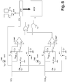
- the figure 8 represents a schema very similar to that of the figure 7 and the common elements will not be re-described; the difference with the figure 7 is the fact that the conversion circuit is intended to provide a numerical value of the average of different but neighboring signal measurements, while the figure 7 was interested in the same signal at different sampling times.
- the input signals are therefore different but the circuits associated with the comparators COMP and COMP 'are identical and operate in the same way.
- the two adjacent pixels provide on two adjacent column conductors COL i and COL i + 1 resetting voltages (Vr i , Vs i ) and then useful voltages (Vr i + 1 , VS i +1 ); the reset voltages are sampled by a common signal SHR; the useful voltages are sampled by an SHS signal.
- the signals corresponding to the column of rank i are applied to the sample-and-hold associated with the comparator COMP, and the signals corresponding to the column of rank i + 1 are applied to the sample-and-hold associated with the comparator COMP '.
- the counter counting at the frequency F counts at the frequency F / 2 from the switchover.
- the contents of the counter are stored. It represents the mean of the measurements of the two pixels (average between the difference VS i - Vr i of the samples coming from the column of rank i and the difference VS i + 1 - Vr i + 1 of the samples coming from the column of rank i + 1).
Landscapes
- Engineering & Computer Science (AREA)
- Theoretical Computer Science (AREA)
- Multimedia (AREA)
- Signal Processing (AREA)
- Analogue/Digital Conversion (AREA)
- Transforming Light Signals Into Electric Signals (AREA)
Claims (9)
- Analog-Digital-Wandlungsverfahren, verwendend einen Rampenwandler, bei welchem:- man an einen Komparator (COMP) ein Paar von zwei Spannungs-Abtastsignalen (Vr1, Vs1) anlegt, wovon eines (Vs1) zu einer linearen Spannungsrampe hinzuaddiert wird,- man in einem Zähler (CNT) Impulse einer Frequenz F von einem Anfangszeitpunkt der Rampe bis zum Kippen des Komparators zählt,dadurch gekennzeichnet, dass:- man an N-1 andere Komparatoren (COMP') N-1 andere Paare von zwei Spannungs-Abtastsignalen (V'r1, Vs1) anlegt, wovon eines (V's1) zu einer linearen Spannungsrampe mit identischem Anfangszeitpunkt und identischer Steigung wie die erste Rampe hinzuaddiert wird, wobei N eine positive Ganzzahl ist,- man an den Zähler eine Zählfrequenz FN-1 anlegt, die so beschaffen ist, dass FN-1 = F(N-1)/N, sobald ein Komparator kippt,- wenn N größer als 2 ist, man nacheinander niedrigere Zählfrequenzen F(N-2)/N, gefolgt von F(N-3)/N an den Zähler anlegt und so weiter bis F/N, jedes Mal, wenn ein Komparator kippt,- und man den Inhalt des Zählers zum Zeitpunkt des Kippens des Komparators, der als letzter kippt, speichert.
- Wandlungsverfahren nach Anspruch 1, dadurch gekennzeichnet, dass N=2 ist.
- Wandlungsverfahren nach einem der vorhergehenden Ansprüche, dadurch gekennzeichnet, dass die Komparatoren Abtastsignale mit einer gleichen Spannungsdifferenz zum Wandeln erhalten, um das Lesegeräusch zu reduzieren.
- Wandlungsverfahren nach Anspruch 3, dadurch gekennzeichnet, dass alle solche Abtastsignale zu unterschiedlichen Zeitpunkten abgenommen werden.
- Wandlungsverfahren nach einem der Ansprüche 1 oder 2, dadurch gekennzeichnet, dass die N Komparatoren gleichzeitige Abtastsignale von N unterschiedlichen Spannungsdifferenzen erhalten und der Wandler einen Wert bereitstellt, der den Durchschnitt dieser N Differenzen bildet.
- Analog-Digital-Rampenwandler, beinhaltend eine Schaltung, welche eine Spannungsrampe etabliert, einen Zähler (CNT), der durch ein Uhrsignal mit einer Frequenz F ab dem Anfangszeitpunkt der Rampe inkrementiert wird, einen Komparator (COMP) zum Vergleichen zweier Spannungs-Abtastsignale der zur Rampe hinzuaddiert wird, dadurch gekennzeichnet, dass der Wandler N-1 andere Komparatoren (COMP') zum Vergleichen von N-1 anderen Spannungs-Abtastsignalen beinhaltet, wovon eines zur einer Rampe hinzuaddiert wird, die mit ersten Rampe identisch ist, eine logische Schaltung zur Zählfrequenzauswahl des Zählers, welche durch die Komparatoren gesteuert wird, zur Auswahl der Frequenz F zu Beginn der Rampe und zur sukzessiven Auswahl der niedrigeren Frequenzen im Zuge des Kippens der Komparatoren, wobei die ausgewählte Frequenz F(N-j)/N ist, wenn j Komparatoren gekippt sind, und ein Mittel (MEM) zum Speichern des Inhaltes des Zählers zum Zeitpunkt des Kippens des Komparators, der als letzter kippt, wobei N eine positive Ganzzahl ist.
- Analog-Digital-Rampenwandler nach Anspruch 6, dadurch gekennzeichnet, dass N=2 ist.
- Matrix-Bildsensor, verwendend einen Wandler nach einem der Ansprüche 6 oder 7, dadurch gekennzeichnet, dass die 2N Spannungs-Abtastsignale durch einen Spaltenleiter (COL) bereitgestellt werden, der die Pixel einer selben Pixel-Spalte verbindet, wobei die Abtastsignale zu unterschiedlichen 2N Zeitpunkten abgenommen werden.
- Matrix-Bildsensor, verwendend einen Wandler nach Anspruch 8, dadurch gekennzeichnet, dass die Spannungs-Abtastsignal-Paare von den jeweiligen Spaltenleitern (COLi, COLi+1) bereitgestellt werden, welche jeden der Pixel einer selben Pixel-Spalte verbinden.
Applications Claiming Priority (2)
| Application Number | Priority Date | Filing Date | Title |
|---|---|---|---|
| FR1454062A FR3020731B1 (fr) | 2014-05-05 | 2014-05-05 | Convertisseur analogique-numerique a rampe apte a fournir directement une moyenne de deux signaux |
| PCT/EP2015/059727 WO2015169755A1 (fr) | 2014-05-05 | 2015-05-04 | Convertisseur analogique-numerique a rampe apte a fournir directement une moyenne de deux signaux |
Publications (2)
| Publication Number | Publication Date |
|---|---|
| EP3140910A1 EP3140910A1 (de) | 2017-03-15 |
| EP3140910B1 true EP3140910B1 (de) | 2018-07-04 |
Family
ID=51570526
Family Applications (1)
| Application Number | Title | Priority Date | Filing Date |
|---|---|---|---|
| EP15723174.7A Active EP3140910B1 (de) | 2014-05-05 | 2015-05-04 | Analog-digital-slope-wandler zur direkten bereitstellung von durchschnittlich zwei signalen |
Country Status (4)
| Country | Link |
|---|---|
| US (1) | US9923571B2 (de) |
| EP (1) | EP3140910B1 (de) |
| FR (1) | FR3020731B1 (de) |
| WO (1) | WO2015169755A1 (de) |
Families Citing this family (3)
| Publication number | Priority date | Publication date | Assignee | Title |
|---|---|---|---|---|
| JP6702821B2 (ja) * | 2016-07-28 | 2020-06-03 | キヤノン株式会社 | 撮像装置及びその制御方法、プログラム、記憶媒体 |
| US10203807B2 (en) | 2017-03-20 | 2019-02-12 | Microsoft Technology Licensing, Llc | Method for sampling output from a grid based digitizer sensor |
| US10546647B2 (en) * | 2017-06-26 | 2020-01-28 | Sandisk Technologies Llc | Wide range zero temperature coefficient oscillators and related devices and methods |
Family Cites Families (4)
| Publication number | Priority date | Publication date | Assignee | Title |
|---|---|---|---|---|
| JP4340296B2 (ja) * | 2007-01-30 | 2009-10-07 | シャープ株式会社 | A/d変換器 |
| KR101448917B1 (ko) * | 2007-09-11 | 2014-10-13 | 삼성전자주식회사 | 의사 멀티플 샘플링 방법을 사용하는 아날로그-디지털 변환장치 및 방법 |
| KR101496712B1 (ko) * | 2008-06-11 | 2015-02-27 | 삼성전자주식회사 | 아날로그-디지털 변환 장치와 이를 포함하는 이미지 촬상 장치 |
| GB2515014B (en) * | 2013-06-10 | 2020-06-17 | Cmosis Bvba | Analog-to-digital conversion |
-
2014
- 2014-05-05 FR FR1454062A patent/FR3020731B1/fr active Active
-
2015
- 2015-05-04 EP EP15723174.7A patent/EP3140910B1/de active Active
- 2015-05-04 US US15/309,259 patent/US9923571B2/en active Active
- 2015-05-04 WO PCT/EP2015/059727 patent/WO2015169755A1/fr not_active Ceased
Non-Patent Citations (1)
| Title |
|---|
| None * |
Also Published As
| Publication number | Publication date |
|---|---|
| FR3020731B1 (fr) | 2016-05-20 |
| FR3020731A1 (fr) | 2015-11-06 |
| EP3140910A1 (de) | 2017-03-15 |
| US20170077943A1 (en) | 2017-03-16 |
| WO2015169755A1 (fr) | 2015-11-12 |
| US9923571B2 (en) | 2018-03-20 |
Similar Documents
| Publication | Publication Date | Title |
|---|---|---|
| EP3058720B1 (de) | Analog-digital-wandler mit einer rampe mt mehreren umwandlungen oder einer einzelnen umwandlung je nach dem durch ein pixel empfangenen lichtpegel | |
| EP2503775B1 (de) | Zweitakt-Bilderfassungsgerät mit Integration und konditioneller Auswahl | |
| US8816893B1 (en) | Adaptive multiple conversion ramp analog-to-digital converter | |
| TWI511562B (zh) | 用於減少像素陣列讀出時間之轉換電路 | |
| EP2064867B1 (de) | Bewegung eines bildsensors mittels sukzessiver integration und summierung mit aktiven cmos-pixeln | |
| CN207369179U (zh) | 模数转换器、模数转换器电路和处理器系统 | |
| EP0006779A1 (de) | Schaltung zur Digitalisierung von einmalig auftretenden Signalen | |
| FR2973162A1 (fr) | Capteur d'image a tres haute dynamique | |
| EP3140910B1 (de) | Analog-digital-slope-wandler zur direkten bereitstellung von durchschnittlich zwei signalen | |
| WO2016180872A1 (fr) | Circuit de lecture d'un capteur a matrice de pixels avec conversion analogique - numerique a haute cadence d'acquisition, et capteur d'images comprenant un tel circuit | |
| EP3021571A1 (de) | Cmos-bildsensor mit analog-digital-umwandlung vom typ sigma-delta | |
| EP2408194B1 (de) | Bilderfassungsgerät mit CMOS-Technologie mit einer starken Videofrequenz | |
| EP3319311A1 (de) | Synchronbildsensor mit zeitkodierung | |
| CA1160726A (fr) | Dispositif pour amplifier et echantillonner des signaux multiplexes | |
| EP2327160B1 (de) | Analogzähler und ein einen solchen zähler enthaltenden bildgeber | |
| EP2214397B1 (de) | Erfassungsschaltung mit Pufferkondensator | |
| EP0749234B1 (de) | Halbleiter-Bildsensor mit integrierte Pixelhistogrammumwandlung | |
| FR2872331A1 (fr) | Echantillonneur analogique rapide pour enregistrement et lecture continus et systeme de conversion numerique | |
| FR2943179A1 (fr) | Capteur d'image mos et procede de lecture avec transistor en regime de faible inversion. | |
| JP5939923B2 (ja) | 固体撮像装置 | |
| EP2446534B1 (de) | Ultrahochpräzise vorrichtung zur messung der zeit eines signaleingangs | |
| FR2574606A1 (fr) | Convertisseur numerique analogique a redistribution de charges capacitives avec autocalibration | |
| FR2896929A1 (fr) | Procede pour realiser la conversion analogique/numerique de signaux, convertisseur mettant en oeuvre ce procede et dispositif de detection de rayonnements electromagnetiques integrant un tel convertisseur | |
| HK1197115B (zh) | 自適應多轉換斜坡模/數轉換器 |
Legal Events
| Date | Code | Title | Description |
|---|---|---|---|
| STAA | Information on the status of an ep patent application or granted ep patent |
Free format text: STATUS: THE INTERNATIONAL PUBLICATION HAS BEEN MADE |
|
| PUAI | Public reference made under article 153(3) epc to a published international application that has entered the european phase |
Free format text: ORIGINAL CODE: 0009012 |
|
| STAA | Information on the status of an ep patent application or granted ep patent |
Free format text: STATUS: REQUEST FOR EXAMINATION WAS MADE |
|
| 17P | Request for examination filed |
Effective date: 20161104 |
|
| AK | Designated contracting states |
Kind code of ref document: A1 Designated state(s): AL AT BE BG CH CY CZ DE DK EE ES FI FR GB GR HR HU IE IS IT LI LT LU LV MC MK MT NL NO PL PT RO RS SE SI SK SM TR |
|
| AX | Request for extension of the european patent |
Extension state: BA ME |
|
| DAV | Request for validation of the european patent (deleted) | ||
| DAX | Request for extension of the european patent (deleted) | ||
| GRAP | Despatch of communication of intention to grant a patent |
Free format text: ORIGINAL CODE: EPIDOSNIGR1 |
|
| STAA | Information on the status of an ep patent application or granted ep patent |
Free format text: STATUS: GRANT OF PATENT IS INTENDED |
|
| INTG | Intention to grant announced |
Effective date: 20180124 |
|
| GRAS | Grant fee paid |
Free format text: ORIGINAL CODE: EPIDOSNIGR3 |
|
| GRAA | (expected) grant |
Free format text: ORIGINAL CODE: 0009210 |
|
| STAA | Information on the status of an ep patent application or granted ep patent |
Free format text: STATUS: THE PATENT HAS BEEN GRANTED |
|
| AK | Designated contracting states |
Kind code of ref document: B1 Designated state(s): AL AT BE BG CH CY CZ DE DK EE ES FI FR GB GR HR HU IE IS IT LI LT LU LV MC MK MT NL NO PL PT RO RS SE SI SK SM TR |
|
| REG | Reference to a national code |
Ref country code: GB Ref legal event code: FG4D Free format text: NOT ENGLISH |
|
| REG | Reference to a national code |
Ref country code: CH Ref legal event code: EP |
|
| REG | Reference to a national code |
Ref country code: AT Ref legal event code: REF Ref document number: 1015595 Country of ref document: AT Kind code of ref document: T Effective date: 20180715 |
|
| REG | Reference to a national code |
Ref country code: IE Ref legal event code: FG4D Free format text: LANGUAGE OF EP DOCUMENT: FRENCH |
|
| REG | Reference to a national code |
Ref country code: DE Ref legal event code: R096 Ref document number: 602015013039 Country of ref document: DE |
|
| REG | Reference to a national code |
Ref country code: NL Ref legal event code: FP |
|
| REG | Reference to a national code |
Ref country code: LT Ref legal event code: MG4D |
|
| REG | Reference to a national code |
Ref country code: AT Ref legal event code: MK05 Ref document number: 1015595 Country of ref document: AT Kind code of ref document: T Effective date: 20180704 |
|
| PG25 | Lapsed in a contracting state [announced via postgrant information from national office to epo] |
Ref country code: CZ Free format text: LAPSE BECAUSE OF FAILURE TO SUBMIT A TRANSLATION OF THE DESCRIPTION OR TO PAY THE FEE WITHIN THE PRESCRIBED TIME-LIMIT Effective date: 20180704 Ref country code: SE Free format text: LAPSE BECAUSE OF FAILURE TO SUBMIT A TRANSLATION OF THE DESCRIPTION OR TO PAY THE FEE WITHIN THE PRESCRIBED TIME-LIMIT Effective date: 20180704 Ref country code: PL Free format text: LAPSE BECAUSE OF FAILURE TO SUBMIT A TRANSLATION OF THE DESCRIPTION OR TO PAY THE FEE WITHIN THE PRESCRIBED TIME-LIMIT Effective date: 20180704 Ref country code: FI Free format text: LAPSE BECAUSE OF FAILURE TO SUBMIT A TRANSLATION OF THE DESCRIPTION OR TO PAY THE FEE WITHIN THE PRESCRIBED TIME-LIMIT Effective date: 20180704 Ref country code: RS Free format text: LAPSE BECAUSE OF FAILURE TO SUBMIT A TRANSLATION OF THE DESCRIPTION OR TO PAY THE FEE WITHIN THE PRESCRIBED TIME-LIMIT Effective date: 20180704 Ref country code: LT Free format text: LAPSE BECAUSE OF FAILURE TO SUBMIT A TRANSLATION OF THE DESCRIPTION OR TO PAY THE FEE WITHIN THE PRESCRIBED TIME-LIMIT Effective date: 20180704 Ref country code: BG Free format text: LAPSE BECAUSE OF FAILURE TO SUBMIT A TRANSLATION OF THE DESCRIPTION OR TO PAY THE FEE WITHIN THE PRESCRIBED TIME-LIMIT Effective date: 20181004 Ref country code: GR Free format text: LAPSE BECAUSE OF FAILURE TO SUBMIT A TRANSLATION OF THE DESCRIPTION OR TO PAY THE FEE WITHIN THE PRESCRIBED TIME-LIMIT Effective date: 20181005 Ref country code: IS Free format text: LAPSE BECAUSE OF FAILURE TO SUBMIT A TRANSLATION OF THE DESCRIPTION OR TO PAY THE FEE WITHIN THE PRESCRIBED TIME-LIMIT Effective date: 20181104 Ref country code: NO Free format text: LAPSE BECAUSE OF FAILURE TO SUBMIT A TRANSLATION OF THE DESCRIPTION OR TO PAY THE FEE WITHIN THE PRESCRIBED TIME-LIMIT Effective date: 20181004 Ref country code: AT Free format text: LAPSE BECAUSE OF FAILURE TO SUBMIT A TRANSLATION OF THE DESCRIPTION OR TO PAY THE FEE WITHIN THE PRESCRIBED TIME-LIMIT Effective date: 20180704 |
|
| PG25 | Lapsed in a contracting state [announced via postgrant information from national office to epo] |
Ref country code: AL Free format text: LAPSE BECAUSE OF FAILURE TO SUBMIT A TRANSLATION OF THE DESCRIPTION OR TO PAY THE FEE WITHIN THE PRESCRIBED TIME-LIMIT Effective date: 20180704 Ref country code: ES Free format text: LAPSE BECAUSE OF FAILURE TO SUBMIT A TRANSLATION OF THE DESCRIPTION OR TO PAY THE FEE WITHIN THE PRESCRIBED TIME-LIMIT Effective date: 20180704 Ref country code: HR Free format text: LAPSE BECAUSE OF FAILURE TO SUBMIT A TRANSLATION OF THE DESCRIPTION OR TO PAY THE FEE WITHIN THE PRESCRIBED TIME-LIMIT Effective date: 20180704 Ref country code: LV Free format text: LAPSE BECAUSE OF FAILURE TO SUBMIT A TRANSLATION OF THE DESCRIPTION OR TO PAY THE FEE WITHIN THE PRESCRIBED TIME-LIMIT Effective date: 20180704 |
|
| REG | Reference to a national code |
Ref country code: DE Ref legal event code: R097 Ref document number: 602015013039 Country of ref document: DE |
|
| PG25 | Lapsed in a contracting state [announced via postgrant information from national office to epo] |
Ref country code: RO Free format text: LAPSE BECAUSE OF FAILURE TO SUBMIT A TRANSLATION OF THE DESCRIPTION OR TO PAY THE FEE WITHIN THE PRESCRIBED TIME-LIMIT Effective date: 20180704 Ref country code: IT Free format text: LAPSE BECAUSE OF FAILURE TO SUBMIT A TRANSLATION OF THE DESCRIPTION OR TO PAY THE FEE WITHIN THE PRESCRIBED TIME-LIMIT Effective date: 20180704 Ref country code: EE Free format text: LAPSE BECAUSE OF FAILURE TO SUBMIT A TRANSLATION OF THE DESCRIPTION OR TO PAY THE FEE WITHIN THE PRESCRIBED TIME-LIMIT Effective date: 20180704 |
|
| PLBE | No opposition filed within time limit |
Free format text: ORIGINAL CODE: 0009261 |
|
| STAA | Information on the status of an ep patent application or granted ep patent |
Free format text: STATUS: NO OPPOSITION FILED WITHIN TIME LIMIT |
|
| PG25 | Lapsed in a contracting state [announced via postgrant information from national office to epo] |
Ref country code: SK Free format text: LAPSE BECAUSE OF FAILURE TO SUBMIT A TRANSLATION OF THE DESCRIPTION OR TO PAY THE FEE WITHIN THE PRESCRIBED TIME-LIMIT Effective date: 20180704 Ref country code: DK Free format text: LAPSE BECAUSE OF FAILURE TO SUBMIT A TRANSLATION OF THE DESCRIPTION OR TO PAY THE FEE WITHIN THE PRESCRIBED TIME-LIMIT Effective date: 20180704 Ref country code: SM Free format text: LAPSE BECAUSE OF FAILURE TO SUBMIT A TRANSLATION OF THE DESCRIPTION OR TO PAY THE FEE WITHIN THE PRESCRIBED TIME-LIMIT Effective date: 20180704 |
|
| 26N | No opposition filed |
Effective date: 20190405 |
|
| PG25 | Lapsed in a contracting state [announced via postgrant information from national office to epo] |
Ref country code: SI Free format text: LAPSE BECAUSE OF FAILURE TO SUBMIT A TRANSLATION OF THE DESCRIPTION OR TO PAY THE FEE WITHIN THE PRESCRIBED TIME-LIMIT Effective date: 20180704 |
|
| REG | Reference to a national code |
Ref country code: CH Ref legal event code: PL |
|
| PG25 | Lapsed in a contracting state [announced via postgrant information from national office to epo] |
Ref country code: MC Free format text: LAPSE BECAUSE OF FAILURE TO SUBMIT A TRANSLATION OF THE DESCRIPTION OR TO PAY THE FEE WITHIN THE PRESCRIBED TIME-LIMIT Effective date: 20180704 Ref country code: LI Free format text: LAPSE BECAUSE OF NON-PAYMENT OF DUE FEES Effective date: 20190531 Ref country code: CH Free format text: LAPSE BECAUSE OF NON-PAYMENT OF DUE FEES Effective date: 20190531 |
|
| PG25 | Lapsed in a contracting state [announced via postgrant information from national office to epo] |
Ref country code: LU Free format text: LAPSE BECAUSE OF NON-PAYMENT OF DUE FEES Effective date: 20190504 |
|
| PG25 | Lapsed in a contracting state [announced via postgrant information from national office to epo] |
Ref country code: TR Free format text: LAPSE BECAUSE OF FAILURE TO SUBMIT A TRANSLATION OF THE DESCRIPTION OR TO PAY THE FEE WITHIN THE PRESCRIBED TIME-LIMIT Effective date: 20180704 |
|
| PG25 | Lapsed in a contracting state [announced via postgrant information from national office to epo] |
Ref country code: IE Free format text: LAPSE BECAUSE OF NON-PAYMENT OF DUE FEES Effective date: 20190504 |
|
| PG25 | Lapsed in a contracting state [announced via postgrant information from national office to epo] |
Ref country code: PT Free format text: LAPSE BECAUSE OF FAILURE TO SUBMIT A TRANSLATION OF THE DESCRIPTION OR TO PAY THE FEE WITHIN THE PRESCRIBED TIME-LIMIT Effective date: 20181104 |
|
| PG25 | Lapsed in a contracting state [announced via postgrant information from national office to epo] |
Ref country code: CY Free format text: LAPSE BECAUSE OF FAILURE TO SUBMIT A TRANSLATION OF THE DESCRIPTION OR TO PAY THE FEE WITHIN THE PRESCRIBED TIME-LIMIT Effective date: 20180704 |
|
| PG25 | Lapsed in a contracting state [announced via postgrant information from national office to epo] |
Ref country code: HU Free format text: LAPSE BECAUSE OF FAILURE TO SUBMIT A TRANSLATION OF THE DESCRIPTION OR TO PAY THE FEE WITHIN THE PRESCRIBED TIME-LIMIT; INVALID AB INITIO Effective date: 20150504 Ref country code: MT Free format text: LAPSE BECAUSE OF FAILURE TO SUBMIT A TRANSLATION OF THE DESCRIPTION OR TO PAY THE FEE WITHIN THE PRESCRIBED TIME-LIMIT Effective date: 20180704 |
|
| PG25 | Lapsed in a contracting state [announced via postgrant information from national office to epo] |
Ref country code: MK Free format text: LAPSE BECAUSE OF FAILURE TO SUBMIT A TRANSLATION OF THE DESCRIPTION OR TO PAY THE FEE WITHIN THE PRESCRIBED TIME-LIMIT Effective date: 20180704 |
|
| PGFP | Annual fee paid to national office [announced via postgrant information from national office to epo] |
Ref country code: NL Payment date: 20250425 Year of fee payment: 11 |
|
| PGFP | Annual fee paid to national office [announced via postgrant information from national office to epo] |
Ref country code: DE Payment date: 20250416 Year of fee payment: 11 |
|
| PGFP | Annual fee paid to national office [announced via postgrant information from national office to epo] |
Ref country code: GB Payment date: 20250417 Year of fee payment: 11 |
|
| PGFP | Annual fee paid to national office [announced via postgrant information from national office to epo] |
Ref country code: BE Payment date: 20250422 Year of fee payment: 11 |
|
| PGFP | Annual fee paid to national office [announced via postgrant information from national office to epo] |
Ref country code: FR Payment date: 20250422 Year of fee payment: 11 |