EP3141519A1 - Procédé de fabrication d'une pièce micromécanique horlogère et ladite pièce micromécanique horlogère - Google Patents
Procédé de fabrication d'une pièce micromécanique horlogère et ladite pièce micromécanique horlogère Download PDFInfo
- Publication number
- EP3141519A1 EP3141519A1 EP15184184.8A EP15184184A EP3141519A1 EP 3141519 A1 EP3141519 A1 EP 3141519A1 EP 15184184 A EP15184184 A EP 15184184A EP 3141519 A1 EP3141519 A1 EP 3141519A1
- Authority
- EP
- European Patent Office
- Prior art keywords
- silicon
- pores
- based substrate
- depth
- diamond
- Prior art date
- Legal status (The legal status is an assumption and is not a legal conclusion. Google has not performed a legal analysis and makes no representation as to the accuracy of the status listed.)
- Granted
Links
Images
Classifications
-
- G—PHYSICS
- G04—HOROLOGY
- G04B—MECHANICALLY-DRIVEN CLOCKS OR WATCHES; MECHANICAL PARTS OF CLOCKS OR WATCHES IN GENERAL; TIME PIECES USING THE POSITION OF THE SUN, MOON OR STARS
- G04B15/00—Escapements
- G04B15/14—Component parts or constructional details, e.g. construction of the lever or the escape wheel
-
- G—PHYSICS
- G04—HOROLOGY
- G04B—MECHANICALLY-DRIVEN CLOCKS OR WATCHES; MECHANICAL PARTS OF CLOCKS OR WATCHES IN GENERAL; TIME PIECES USING THE POSITION OF THE SUN, MOON OR STARS
- G04B13/00—Gearwork
- G04B13/02—Wheels; Pinions; Spindles; Pivots
- G04B13/021—Wheels; Pinions; Spindles; Pivots elastic fitting with a spindle, axis or shaft
- G04B13/022—Wheels; Pinions; Spindles; Pivots elastic fitting with a spindle, axis or shaft with parts made of hard material, e.g. silicon, diamond, sapphire, quartz and the like
-
- G—PHYSICS
- G04—HOROLOGY
- G04D—APPARATUS OR TOOLS SPECIALLY DESIGNED FOR MAKING OR MAINTAINING CLOCKS OR WATCHES
- G04D3/00—Watchmakers' or watch-repairers' machines or tools for working materials
- G04D3/0002—Watchmakers' or watch-repairers' machines or tools for working materials for mechanical working other than with a lathe
- G04D3/0028—Watchmakers' or watch-repairers' machines or tools for working materials for mechanical working other than with a lathe for components of the escape mechanism
- G04D3/003—Watchmakers' or watch-repairers' machines or tools for working materials for mechanical working other than with a lathe for components of the escape mechanism for levers
-
- B—PERFORMING OPERATIONS; TRANSPORTING
- B32—LAYERED PRODUCTS
- B32B—LAYERED PRODUCTS, i.e. PRODUCTS BUILT-UP OF STRATA OF FLAT OR NON-FLAT, e.g. CELLULAR OR HONEYCOMB, FORM
- B32B17/00—Layered products essentially comprising sheet glass, or glass, slag, or like fibres
- B32B17/06—Layered products essentially comprising sheet glass, or glass, slag, or like fibres comprising glass as the main or only constituent of a layer, next to another layer of a specific material
- B32B17/10—Layered products essentially comprising sheet glass, or glass, slag, or like fibres comprising glass as the main or only constituent of a layer, next to another layer of a specific material of synthetic resin
- B32B17/10005—Layered products essentially comprising sheet glass, or glass, slag, or like fibres comprising glass as the main or only constituent of a layer, next to another layer of a specific material of synthetic resin laminated safety glass or glazing
- B32B17/1055—Layered products essentially comprising sheet glass, or glass, slag, or like fibres comprising glass as the main or only constituent of a layer, next to another layer of a specific material of synthetic resin laminated safety glass or glazing characterized by the resin layer, i.e. interlayer
- B32B17/10798—Layered products essentially comprising sheet glass, or glass, slag, or like fibres comprising glass as the main or only constituent of a layer, next to another layer of a specific material of synthetic resin laminated safety glass or glazing characterized by the resin layer, i.e. interlayer containing silicone
-
- B—PERFORMING OPERATIONS; TRANSPORTING
- B81—MICROSTRUCTURAL TECHNOLOGY
- B81B—MICROSTRUCTURAL DEVICES OR SYSTEMS, e.g. MICROMECHANICAL DEVICES
- B81B3/00—Devices comprising flexible or deformable elements, e.g. comprising elastic tongues or membranes
- B81B3/0064—Constitution or structural means for improving or controlling the physical properties of a device
- B81B3/0067—Mechanical properties
- B81B3/007—For controlling stiffness, e.g. ribs
-
- B—PERFORMING OPERATIONS; TRANSPORTING
- B81—MICROSTRUCTURAL TECHNOLOGY
- B81C—PROCESSES OR APPARATUS SPECIALLY ADAPTED FOR THE MANUFACTURE OR TREATMENT OF MICROSTRUCTURAL DEVICES OR SYSTEMS
- B81C1/00—Manufacture or treatment of devices or systems in or on a substrate
- B81C1/00349—Creating layers of material on a substrate
- B81C1/0038—Processes for creating layers of materials not provided for in groups B81C1/00357 - B81C1/00373
-
- B—PERFORMING OPERATIONS; TRANSPORTING
- B81—MICROSTRUCTURAL TECHNOLOGY
- B81C—PROCESSES OR APPARATUS SPECIALLY ADAPTED FOR THE MANUFACTURE OR TREATMENT OF MICROSTRUCTURAL DEVICES OR SYSTEMS
- B81C1/00—Manufacture or treatment of devices or systems in or on a substrate
- B81C1/00436—Shaping materials, i.e. techniques for structuring the substrate or the layers on the substrate
- B81C1/00523—Etching material
- B81C1/00539—Wet etching
-
- B—PERFORMING OPERATIONS; TRANSPORTING
- B81—MICROSTRUCTURAL TECHNOLOGY
- B81C—PROCESSES OR APPARATUS SPECIALLY ADAPTED FOR THE MANUFACTURE OR TREATMENT OF MICROSTRUCTURAL DEVICES OR SYSTEMS
- B81C1/00—Manufacture or treatment of devices or systems in or on a substrate
- B81C1/00436—Shaping materials, i.e. techniques for structuring the substrate or the layers on the substrate
- B81C1/00523—Etching material
- B81C1/00547—Etching processes not provided for in groups B81C1/00531 - B81C1/00539
-
- B—PERFORMING OPERATIONS; TRANSPORTING
- B81—MICROSTRUCTURAL TECHNOLOGY
- B81C—PROCESSES OR APPARATUS SPECIALLY ADAPTED FOR THE MANUFACTURE OR TREATMENT OF MICROSTRUCTURAL DEVICES OR SYSTEMS
- B81C99/00—Subject matter not provided for in other groups of this subclass
- B81C99/0075—Manufacture of substrate-free structures
- B81C99/0085—Manufacture of substrate-free structures using moulds and master templates, e.g. for hot-embossing
-
- G—PHYSICS
- G04—HOROLOGY
- G04B—MECHANICALLY-DRIVEN CLOCKS OR WATCHES; MECHANICAL PARTS OF CLOCKS OR WATCHES IN GENERAL; TIME PIECES USING THE POSITION OF THE SUN, MOON OR STARS
- G04B13/00—Gearwork
- G04B13/02—Wheels; Pinions; Spindles; Pivots
-
- G—PHYSICS
- G04—HOROLOGY
- G04B—MECHANICALLY-DRIVEN CLOCKS OR WATCHES; MECHANICAL PARTS OF CLOCKS OR WATCHES IN GENERAL; TIME PIECES USING THE POSITION OF THE SUN, MOON OR STARS
- G04B17/00—Mechanisms for stabilising frequency
- G04B17/04—Oscillators acting by spring tension
- G04B17/06—Oscillators with hairsprings, e.g. balance
- G04B17/066—Manufacture of the spiral spring
-
- G—PHYSICS
- G04—HOROLOGY
- G04B—MECHANICALLY-DRIVEN CLOCKS OR WATCHES; MECHANICAL PARTS OF CLOCKS OR WATCHES IN GENERAL; TIME PIECES USING THE POSITION OF THE SUN, MOON OR STARS
- G04B18/00—Mechanisms for setting frequency
- G04B18/08—Component parts or constructional details
-
- G—PHYSICS
- G04—HOROLOGY
- G04B—MECHANICALLY-DRIVEN CLOCKS OR WATCHES; MECHANICAL PARTS OF CLOCKS OR WATCHES IN GENERAL; TIME PIECES USING THE POSITION OF THE SUN, MOON OR STARS
- G04B31/00—Bearings; Point suspensions or counter-point suspensions; Pivot bearings; Single parts therefor
- G04B31/004—Bearings; Point suspensions or counter-point suspensions; Pivot bearings; Single parts therefor characterised by the material used
-
- G—PHYSICS
- G04—HOROLOGY
- G04D—APPARATUS OR TOOLS SPECIALLY DESIGNED FOR MAKING OR MAINTAINING CLOCKS OR WATCHES
- G04D3/00—Watchmakers' or watch-repairers' machines or tools for working materials
-
- G—PHYSICS
- G04—HOROLOGY
- G04D—APPARATUS OR TOOLS SPECIALLY DESIGNED FOR MAKING OR MAINTAINING CLOCKS OR WATCHES
- G04D3/00—Watchmakers' or watch-repairers' machines or tools for working materials
- G04D3/0002—Watchmakers' or watch-repairers' machines or tools for working materials for mechanical working other than with a lathe
- G04D3/0028—Watchmakers' or watch-repairers' machines or tools for working materials for mechanical working other than with a lathe for components of the escape mechanism
- G04D3/0033—Watchmakers' or watch-repairers' machines or tools for working materials for mechanical working other than with a lathe for components of the escape mechanism for lever wheels
-
- G—PHYSICS
- G04—HOROLOGY
- G04D—APPARATUS OR TOOLS SPECIALLY DESIGNED FOR MAKING OR MAINTAINING CLOCKS OR WATCHES
- G04D3/00—Watchmakers' or watch-repairers' machines or tools for working materials
- G04D3/0069—Watchmakers' or watch-repairers' machines or tools for working materials for working with non-mechanical means, e.g. chemical, electrochemical, metallising, vapourising; with electron beams, laser beams
-
- B—PERFORMING OPERATIONS; TRANSPORTING
- B81—MICROSTRUCTURAL TECHNOLOGY
- B81B—MICROSTRUCTURAL DEVICES OR SYSTEMS, e.g. MICROMECHANICAL DEVICES
- B81B2201/00—Specific applications of microelectromechanical systems
- B81B2201/03—Microengines and actuators
- B81B2201/035—Microgears
-
- B—PERFORMING OPERATIONS; TRANSPORTING
- B81—MICROSTRUCTURAL TECHNOLOGY
- B81C—PROCESSES OR APPARATUS SPECIALLY ADAPTED FOR THE MANUFACTURE OR TREATMENT OF MICROSTRUCTURAL DEVICES OR SYSTEMS
- B81C1/00—Manufacture or treatment of devices or systems in or on a substrate
- B81C1/00642—Manufacture or treatment of devices or systems in or on a substrate for improving the physical properties of a device
- B81C1/00714—Treatment for improving the physical properties not provided for in groups B81C1/0065 - B81C1/00706
-
- B—PERFORMING OPERATIONS; TRANSPORTING
- B81—MICROSTRUCTURAL TECHNOLOGY
- B81C—PROCESSES OR APPARATUS SPECIALLY ADAPTED FOR THE MANUFACTURE OR TREATMENT OF MICROSTRUCTURAL DEVICES OR SYSTEMS
- B81C1/00—Manufacture or treatment of devices or systems in or on a substrate
- B81C1/00912—Treatments or methods for avoiding stiction of flexible or moving parts of MEMS
- B81C1/00992—Treatments or methods for avoiding stiction of flexible or moving parts of MEMS not provided for in groups B81C1/0092 - B81C1/00984
-
- B—PERFORMING OPERATIONS; TRANSPORTING
- B81—MICROSTRUCTURAL TECHNOLOGY
- B81C—PROCESSES OR APPARATUS SPECIALLY ADAPTED FOR THE MANUFACTURE OR TREATMENT OF MICROSTRUCTURAL DEVICES OR SYSTEMS
- B81C2201/00—Manufacture or treatment of microstructural devices or systems
- B81C2201/01—Manufacture or treatment of microstructural devices or systems in or on a substrate
- B81C2201/0101—Shaping material; Structuring the bulk substrate or layers on the substrate; Film patterning
- B81C2201/0111—Bulk micromachining
- B81C2201/0115—Porous silicon
-
- B—PERFORMING OPERATIONS; TRANSPORTING
- B81—MICROSTRUCTURAL TECHNOLOGY
- B81C—PROCESSES OR APPARATUS SPECIALLY ADAPTED FOR THE MANUFACTURE OR TREATMENT OF MICROSTRUCTURAL DEVICES OR SYSTEMS
- B81C2201/00—Manufacture or treatment of microstructural devices or systems
- B81C2201/03—Processes for manufacturing substrate-free structures
- B81C2201/034—Moulding
-
- C—CHEMISTRY; METALLURGY
- C09—DYES; PAINTS; POLISHES; NATURAL RESINS; ADHESIVES; COMPOSITIONS NOT OTHERWISE PROVIDED FOR; APPLICATIONS OF MATERIALS NOT OTHERWISE PROVIDED FOR
- C09K—MATERIALS FOR MISCELLANEOUS APPLICATIONS, NOT PROVIDED FOR ELSEWHERE
- C09K13/00—Etching, surface-brightening or pickling compositions
-
- C—CHEMISTRY; METALLURGY
- C09—DYES; PAINTS; POLISHES; NATURAL RESINS; ADHESIVES; COMPOSITIONS NOT OTHERWISE PROVIDED FOR; APPLICATIONS OF MATERIALS NOT OTHERWISE PROVIDED FOR
- C09K—MATERIALS FOR MISCELLANEOUS APPLICATIONS, NOT PROVIDED FOR ELSEWHERE
- C09K13/00—Etching, surface-brightening or pickling compositions
- C09K13/04—Etching, surface-brightening or pickling compositions containing an inorganic acid
- C09K13/08—Etching, surface-brightening or pickling compositions containing an inorganic acid containing a fluorine compound
-
- C—CHEMISTRY; METALLURGY
- C23—COATING METALLIC MATERIAL; COATING MATERIAL WITH METALLIC MATERIAL; CHEMICAL SURFACE TREATMENT; DIFFUSION TREATMENT OF METALLIC MATERIAL; COATING BY VACUUM EVAPORATION, BY SPUTTERING, BY ION IMPLANTATION OR BY CHEMICAL VAPOUR DEPOSITION, IN GENERAL; INHIBITING CORROSION OF METALLIC MATERIAL OR INCRUSTATION IN GENERAL
- C23C—COATING METALLIC MATERIAL; COATING MATERIAL WITH METALLIC MATERIAL; SURFACE TREATMENT OF METALLIC MATERIAL BY DIFFUSION INTO THE SURFACE, BY CHEMICAL CONVERSION OR SUBSTITUTION; COATING BY VACUUM EVAPORATION, BY SPUTTERING, BY ION IMPLANTATION OR BY CHEMICAL VAPOUR DEPOSITION, IN GENERAL
- C23C14/00—Coating by vacuum evaporation, by sputtering or by ion implantation of the coating forming material
- C23C14/06—Coating by vacuum evaporation, by sputtering or by ion implantation of the coating forming material characterised by the coating material
- C23C14/0605—Carbon
- C23C14/0611—Diamond
-
- C—CHEMISTRY; METALLURGY
- C23—COATING METALLIC MATERIAL; COATING MATERIAL WITH METALLIC MATERIAL; CHEMICAL SURFACE TREATMENT; DIFFUSION TREATMENT OF METALLIC MATERIAL; COATING BY VACUUM EVAPORATION, BY SPUTTERING, BY ION IMPLANTATION OR BY CHEMICAL VAPOUR DEPOSITION, IN GENERAL; INHIBITING CORROSION OF METALLIC MATERIAL OR INCRUSTATION IN GENERAL
- C23C—COATING METALLIC MATERIAL; COATING MATERIAL WITH METALLIC MATERIAL; SURFACE TREATMENT OF METALLIC MATERIAL BY DIFFUSION INTO THE SURFACE, BY CHEMICAL CONVERSION OR SUBSTITUTION; COATING BY VACUUM EVAPORATION, BY SPUTTERING, BY ION IMPLANTATION OR BY CHEMICAL VAPOUR DEPOSITION, IN GENERAL
- C23C14/00—Coating by vacuum evaporation, by sputtering or by ion implantation of the coating forming material
- C23C14/06—Coating by vacuum evaporation, by sputtering or by ion implantation of the coating forming material characterised by the coating material
- C23C14/0641—Nitrides
- C23C14/0652—Silicon nitride
-
- C—CHEMISTRY; METALLURGY
- C23—COATING METALLIC MATERIAL; COATING MATERIAL WITH METALLIC MATERIAL; CHEMICAL SURFACE TREATMENT; DIFFUSION TREATMENT OF METALLIC MATERIAL; COATING BY VACUUM EVAPORATION, BY SPUTTERING, BY ION IMPLANTATION OR BY CHEMICAL VAPOUR DEPOSITION, IN GENERAL; INHIBITING CORROSION OF METALLIC MATERIAL OR INCRUSTATION IN GENERAL
- C23C—COATING METALLIC MATERIAL; COATING MATERIAL WITH METALLIC MATERIAL; SURFACE TREATMENT OF METALLIC MATERIAL BY DIFFUSION INTO THE SURFACE, BY CHEMICAL CONVERSION OR SUBSTITUTION; COATING BY VACUUM EVAPORATION, BY SPUTTERING, BY ION IMPLANTATION OR BY CHEMICAL VAPOUR DEPOSITION, IN GENERAL
- C23C14/00—Coating by vacuum evaporation, by sputtering or by ion implantation of the coating forming material
- C23C14/06—Coating by vacuum evaporation, by sputtering or by ion implantation of the coating forming material characterised by the coating material
- C23C14/10—Glass or silica
-
- C—CHEMISTRY; METALLURGY
- C23—COATING METALLIC MATERIAL; COATING MATERIAL WITH METALLIC MATERIAL; CHEMICAL SURFACE TREATMENT; DIFFUSION TREATMENT OF METALLIC MATERIAL; COATING BY VACUUM EVAPORATION, BY SPUTTERING, BY ION IMPLANTATION OR BY CHEMICAL VAPOUR DEPOSITION, IN GENERAL; INHIBITING CORROSION OF METALLIC MATERIAL OR INCRUSTATION IN GENERAL
- C23C—COATING METALLIC MATERIAL; COATING MATERIAL WITH METALLIC MATERIAL; SURFACE TREATMENT OF METALLIC MATERIAL BY DIFFUSION INTO THE SURFACE, BY CHEMICAL CONVERSION OR SUBSTITUTION; COATING BY VACUUM EVAPORATION, BY SPUTTERING, BY ION IMPLANTATION OR BY CHEMICAL VAPOUR DEPOSITION, IN GENERAL
- C23C14/00—Coating by vacuum evaporation, by sputtering or by ion implantation of the coating forming material
- C23C14/06—Coating by vacuum evaporation, by sputtering or by ion implantation of the coating forming material characterised by the coating material
- C23C14/12—Organic material
-
- C—CHEMISTRY; METALLURGY
- C23—COATING METALLIC MATERIAL; COATING MATERIAL WITH METALLIC MATERIAL; CHEMICAL SURFACE TREATMENT; DIFFUSION TREATMENT OF METALLIC MATERIAL; COATING BY VACUUM EVAPORATION, BY SPUTTERING, BY ION IMPLANTATION OR BY CHEMICAL VAPOUR DEPOSITION, IN GENERAL; INHIBITING CORROSION OF METALLIC MATERIAL OR INCRUSTATION IN GENERAL
- C23C—COATING METALLIC MATERIAL; COATING MATERIAL WITH METALLIC MATERIAL; SURFACE TREATMENT OF METALLIC MATERIAL BY DIFFUSION INTO THE SURFACE, BY CHEMICAL CONVERSION OR SUBSTITUTION; COATING BY VACUUM EVAPORATION, BY SPUTTERING, BY ION IMPLANTATION OR BY CHEMICAL VAPOUR DEPOSITION, IN GENERAL
- C23C16/00—Chemical coating by decomposition of gaseous compounds, without leaving reaction products of surface material in the coating, i.e. chemical vapour deposition [CVD] processes
- C23C16/02—Pretreatment of the material to be coated
- C23C16/0254—Physical treatment to alter the texture of the surface, e.g. scratching or polishing
-
- C—CHEMISTRY; METALLURGY
- C23—COATING METALLIC MATERIAL; COATING MATERIAL WITH METALLIC MATERIAL; CHEMICAL SURFACE TREATMENT; DIFFUSION TREATMENT OF METALLIC MATERIAL; COATING BY VACUUM EVAPORATION, BY SPUTTERING, BY ION IMPLANTATION OR BY CHEMICAL VAPOUR DEPOSITION, IN GENERAL; INHIBITING CORROSION OF METALLIC MATERIAL OR INCRUSTATION IN GENERAL
- C23C—COATING METALLIC MATERIAL; COATING MATERIAL WITH METALLIC MATERIAL; SURFACE TREATMENT OF METALLIC MATERIAL BY DIFFUSION INTO THE SURFACE, BY CHEMICAL CONVERSION OR SUBSTITUTION; COATING BY VACUUM EVAPORATION, BY SPUTTERING, BY ION IMPLANTATION OR BY CHEMICAL VAPOUR DEPOSITION, IN GENERAL
- C23C16/00—Chemical coating by decomposition of gaseous compounds, without leaving reaction products of surface material in the coating, i.e. chemical vapour deposition [CVD] processes
- C23C16/44—Chemical coating by decomposition of gaseous compounds, without leaving reaction products of surface material in the coating, i.e. chemical vapour deposition [CVD] processes characterised by the method of coating
- C23C16/455—Chemical coating by decomposition of gaseous compounds, without leaving reaction products of surface material in the coating, i.e. chemical vapour deposition [CVD] processes characterised by the method of coating characterised by the method used for introducing gases into reaction chamber or for modifying gas flows in reaction chamber
- C23C16/45523—Pulsed gas flow or change of composition over time
- C23C16/45525—Atomic layer deposition [ALD]
-
- C—CHEMISTRY; METALLURGY
- C25—ELECTROLYTIC OR ELECTROPHORETIC PROCESSES; APPARATUS THEREFOR
- C25F—PROCESSES FOR THE ELECTROLYTIC REMOVAL OF MATERIALS FROM OBJECTS; APPARATUS THEREFOR
- C25F3/00—Electrolytic etching or polishing
- C25F3/02—Etching
-
- C—CHEMISTRY; METALLURGY
- C25—ELECTROLYTIC OR ELECTROPHORETIC PROCESSES; APPARATUS THEREFOR
- C25F—PROCESSES FOR THE ELECTROLYTIC REMOVAL OF MATERIALS FROM OBJECTS; APPARATUS THEREFOR
- C25F3/00—Electrolytic etching or polishing
- C25F3/02—Etching
- C25F3/12—Etching of semiconducting materials
Definitions
- the present invention relates to a method for producing reinforced micromechanical watch parts, based on silicon.
- the invention also relates to a reinforced micromechanical watchmaking component, based on silicon, which can in particular be obtained by such a method.
- Silicon is a material that is increasingly used in the manufacture of micromechanical watchmaking parts, in particular parts that remain connected to a silicon-based substrate on which they have been machined.
- silicon Compared to the metals or alloys conventionally used to manufacture micromechanical watch parts, such as gears, or the components of the exhaust, silicon has many advantages. It is a very hard material, of a very light weight which allows it to present a very reduced inertia and consequently to improve the yield. Silicon also makes it possible to produce complex parts, or monobloc.
- silicon is deposited on the diamond, for example by a thin-layer vapor phase deposition (CVD / PVD) method.
- CVD / PVD thin-layer vapor phase deposition
- the present invention also relates to a watchmaking micromechanical component that can be obtained by the method as defined above.
- the present invention also relates to a watchmaking micromechanical component comprising a silicon-based substrate which has, on the surface of at least a portion of one of its surfaces, pores of a given depth, said pores being entirely filled with a layer of a material chosen from diamond, diamond-carbon (DLC), silicon oxide, silicon nitride, ceramics, polymers and their mixtures, of a thickness at least equal to the depth of the pores.
- a material chosen from diamond, diamond-carbon (DLC), silicon oxide, silicon nitride, ceramics, polymers and their mixtures of a thickness at least equal to the depth of the pores.
- the part may comprise a surface layer of said material on the surface of the silicon-based substrate and pores filled with the material.
- the method according to the invention makes it possible, by virtue of the prior formation of pores on the surface of the substrate, to create a real substrate surface much greater than the initial surface, and consequently to greatly increase the apparent deposition rate of a substrate. appropriate material.
- the method according to the invention makes it possible, on the surface of the silicon-based substrate, to manufacture a thick layer of a suitable material in a fast time, greatly reduced compared to a deposit on the flat surface of a similar substrate. but not porous.
- the method for producing a micromechanical watchmaking component from a silicon-based substrate firstly comprises a step a) for the formation of pores of a determined depth, starting from the surface of at least a portion of a surface of said silicon-based substrate, said pores opening at the outer surface of the silicon-based substrate.
- the silicon-based substrate is chosen as a function of the watchmaking micromechanical component to be formed.
- the final shape of the silicon-based substrate as a function of the watchmaking micromechanical component to be manufactured is given before or after the implementation of the method of the invention.
- the term "silicon-based substrate” refers both to a silicon layer in a substrate and to a substrate. silicon substrate.
- the silicon-based substrate 1 is a silicon wafer or an SOI wafer (Silicon-on-Insulator).
- the pores may be formed both on the surface parallel to the plane of the substrate and on the surface perpendicular to the plane of the substrate.
- this step a) can be carried out by a process chosen from the group comprising an electrochemical etching process, a "Stain-etch” type method, and a "MAC-Etch” type process.
- the electrochemical etching process may be an electrochemical anodizing process. Its implementation requires the use of an electrochemical bath containing hydrofluoric acid in aqueous solution or mixed with ethanol in concentrations of 1 to 10%. Electrical current and electrodes are needed to create electrochemical conditions inducing silicon attack. Depending on the electrochemical conditions, different types of pores can be obtained. Such a method is known to those skilled in the art and does not require detailed information here.
- the "Stain-etch" type process is based on a wet etching of silicon resulting directly in the formation of porous silicon.
- the attack is carried out with a HF / HNO 3 / H 2 O solution with a HF: HNO 3 ratio of 50-500: 1.
- This method has the advantage of not requiring electrical input into the bath. Such a method is known to those skilled in the art and does not require detailed information here.
- step a) is carried out by a method of the "MAC-Etch” type.
- This process is based on the use of noble metal particles to catalyze local chemical attack reactions.
- a very thin layer (10-50 nm) of a noble metal gold, silver, platinum
- the noble metal is gold.
- the particle size may be between 5 and 1000 nm.
- the structuring can be obtained by lithography of gold, attack or lift-off.
- Another option is evaporation or sputtering of a very thin, non-closed layer (5-30 nm). Heat treatment may contribute to the formation of islands of gold.
- the noble metal When the silicon with the noble metal layer is immersed in an aqueous solution of a HF / H 2 O 2 mixture, the noble metal locally catalyzes the dissolution of the silicon.
- This etching solution can typically comprise between 4 ml: 1 ml: 8 ml (48% HF: 30% H 2 O 2 : H 2 O) and 4 ml: 1 ml: 40 ml (48% HF: 30% H 2 O 2 : H 2 O). Silicon dissolution occurs preferentially under the metal, which then gradually sinks into the silicon. This reaction can be continued over great depths (> 100 m ⁇ ) according to propagation modes essentially influenced by the orientation of the silicon crystal, the surface arrangement, the doping and the bath chemistry.
- the method of "MAC-Etch” type has the advantage of not requiring electrical input into the bath while allowing the formation of very deep pores (> 100 m ⁇ ) in the silicon. It is therefore particularly suitable for the use, as a substrate, of SOI wafers generally used for the manufacture of watch components.
- the pores may advantageously have an aspect ratio (depth to diameter ratio) of less than or equal to 100: 1.
- the aspect ratio of the pores in the silicon-based substrate is preferably less than or equal to 4: 1.
- the aspect factor of The pores in the silicon-based substrate is preferably less than or equal to 50: 1.
- the pores may have a depth greater than 100 ⁇ m, preferably greater than 200 ⁇ m and more preferably greater than 300 ⁇ m.
- the formation of pores 2 in the silicon-based substrate 1 to a certain depth results in the formation, between the pores 2, of pillars 3 based on silicon on the same depth.
- the pores 2 are formed so that the projected area of the pillars 3 based on silicon is less than 79% of the apparent total area so as not to have of touching silicon-based pillars, which would stiffen the structure (this corresponds to the percolation threshold).
- the second step b) of the process according to the invention consists in completely filling the pores formed in the silicon-based substrate during step a), of a material chosen from diamond, diamond-carbon (DLC), silicon oxide, silicon nitride, ceramics, polymers and mixtures thereof, in order to form in the pores a layer of said material having a thickness at least equal to the depth of the pores.
- a material chosen from diamond, diamond-carbon (DLC), silicon oxide, silicon nitride, ceramics, polymers and mixtures thereof in order to form in the pores a layer of said material having a thickness at least equal to the depth of the pores.
- This second step b) is carried out directly after step a), without any intermediate step, so that the material deposited in the pores is in direct contact with the walls of said pores.
- step b) is carried out by a process selected from the group consisting of thin-layer deposition processes, such as chemical vapor deposition (CVD), physical vapor deposition (PVD), deposition atomic thin films (ALD), and thermal oxidation.
- CVD chemical vapor deposition
- PVD physical vapor deposition
- ALD deposition atomic thin films
- thermal oxidation thermal oxidation
- the deposit rate will preferably be included between 0.1 and 5 nm / s.
- the deposition rate will preferably be between 0.01 and 10 nm / s.
- ALD deposition atomic thin films
- thermal oxidation is particularly advantageous for reducing the proportion of silicon in a silicon substrate, the silicon being consumed by growth at about 50% of the thickness of the layer.
- thermal oxidation is particularly advantageous for reducing the proportion of silicon in a silicon substrate, the silicon being consumed by growth at about 50% of the thickness of the layer.
- the method according to the invention comprises, after step b), a step c) of forming a surface layer of said material on the surface of the substrate and pores filled with the material. More particularly, this surface layer can be obtained by extending the deposition of the material according to step b) so as not only to completely fill the pores 2 of the material but also to then deposit said material on the pores 2 filled with the material as well as on the pillars 3 to form a solid layer 4 of said material of thickness h0, as shown in FIG. figure 3 .
- a ratio h0 / h1 of the order of 10% may be obtained.
- the method according to the invention makes it possible to obtain a micromechanical watchmaking component comprising a thick composite layer based on silicon / deposited material, or even a thick layer of deposited material when all the silicon has been replaced.
- the method according to the invention makes it possible to obtain a silicon / deposited material composite layer of thickness h1 in a deposition time close to that required to obtain a layer solid material thickness h0 corresponding to the surface layer 4.
- the method according to the invention can advantageously be implemented for the manufacture of silicon-based exhaust components, such as the escape wheel and the anchor, by forming thick layers of diamond by CVD.
- the method according to the invention can also be used for the manufacture of silicon-based exhaust components, by forming thick layers of SiO 2, which are almost solid if the thermal oxidation process is used for SiO 2 deposition.
- the method according to the invention can also be used to quickly create very deep local layers deep in the silicon, combining it with the structuring of porous silicon zones.
Landscapes
- Physics & Mathematics (AREA)
- Engineering & Computer Science (AREA)
- General Physics & Mathematics (AREA)
- Microelectronics & Electronic Packaging (AREA)
- Manufacturing & Machinery (AREA)
- Mechanical Engineering (AREA)
- Computer Hardware Design (AREA)
- Optics & Photonics (AREA)
- Plasma & Fusion (AREA)
- Micromachines (AREA)
- Metallurgy (AREA)
- Physical Vapour Deposition (AREA)
Abstract
Description
- La présente invention se rapporte à un procédé pour produire des pièces micromécaniques horlogères renforcées, à base de silicium. L'invention se rapporte également à une pièce micromécanique horlogère renforcée, à base de silicium, pouvant notamment être obtenue par un tel procédé.
- Le silicium est un matériau de plus en plus utilisé dans la fabrication de pièces micromécaniques horlogères, notamment des pièces qui restent liées à un substrat à base de silicium sur lequel elles ont été usinées.
- Par rapport aux métaux ou alliages classiquement utilisés pour fabriquer des pièces micromécaniques horlogères, telles que des roues dentées, ou les composants de l'échappement, le silicium présente de nombreux avantages. C'est un matériau très dur, d'un poids très léger qui lui permet donc de présenter une inertie très réduite et en conséquence d'améliorer le rendement. Le silicium permet également de réaliser des pièces complexes, ou monobloc.
- Afin d'améliorer ou modifier les propriétés du silicium, il est connu de déposer sur le silicium une couche d'un matériau approprié. Ainsi, pour améliorer ses propriétés tribologiques, on dépose sur le silicium du diamant, par exemple par un procédé de dépôts de couche mince en phase vapeur (CVD/PVD).
- Toutefois, ces procédés présentent un taux de dépôt qui peut s'avérer trop lent lorsque l'épaisseur de la couche déposée dépasse quelques microns. En effet, les taux de dépôts dans les machines CVD par exemple étant typiquement de l'ordre de la dizaine de nanomètre/minute, cette technique n'est généralement pas utilisée pour la fabrication de couche supérieure à quelques microns.
- Il est donc nécessaire de proposer un procédé de fabrication d'une pièce micromécanique horlogère à base de silicium permettant de réaliser des dépôts rapides de couches épaisses d'un matériau approprié sur le silicium.
- A cet effet, la présente invention concerne un procédé de fabrication d'une pièce micromécanique horlogère à partir d'un substrat à base de silicium, comprenant, dans l'ordre, les étapes de :
- a) former des pores à la surface d'au moins une partie d'une surface dudit substrat à base de silicium d'une profondeur déterminée,
- b) remplir entièrement lesdits pores d'un matériau choisi parmi le diamant, le carbone-diamant (DLC), l'oxyde de silicium, le nitrure de silicium, des céramiques, des polymères et leurs mélanges, afin de former dans les pores une couche dudit matériau d'une épaisseur au moins égale à la profondeur des pores.
- La présente invention concerne également une pièce micromécanique horlogère susceptible d'être obtenue par le procédé tel que défini ci-dessus.
- La présente invention concerne également une pièce micromécanique horlogère comprenant un substrat à base de silicium qui présente, à la surface d'au moins une partie d'une de ses surfaces, des pores d'une profondeur déterminée, lesdits pores étant entièrement remplis d'une couche d'un matériau choisi parmi le diamant, le carbone-diamant (DLC), l'oxyde de silicium, le nitrure de silicium, des céramiques, des polymères et leurs mélanges, d'une épaisseur au moins égale à la profondeur des pores.
- D'une manière avantageuse, la pièce peut comprendre une couche de surface dudit matériau à la surface du substrat à base de silicium et des pores remplis du matériau.
- Le procédé selon l'invention permet, grâce à la formation préalable de pores à la surface du substrat, de créer une surface réelle de substrat très supérieure à la surface initiale, et en conséquence d'accroitre fortement le taux de dépôt apparent d'un matériau approprié. Ainsi, le procédé selon l'invention permet de fabriquer, en surface du substrat à base de silicium, une couche épaisse d'un matériau approprié en un temps rapide, fortement réduit par rapport à un dépôt sur la surface plane d'un substrat similaire, mais non poreux.
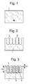
- Les buts, avantages et caractéristiques de la présente invention apparaîtront plus clairement dans la description détaillée suivante d'au moins une forme de réalisation de l'invention donnée uniquement à titre d'exemple non limitatif et illustrée par les dessins annexés sur lesquels :
- les
figures 1 à 3 illustrent schématiquement les étapes d'un procédé de fabrication selon l'invention. - Le procédé de fabrication d'une pièce micromécanique horlogère à partir d'un substrat à base de silicium selon l'invention comprend tout d'abord une étape a) de formation de pores d'une profondeur déterminée, à partir de la surface d'au moins une partie d'une surface dudit substrat à base de silicium, lesdits pores débouchant à la surface externe du substrat à base de silicium. Le substrat à base de silicium est choisi en fonction de la pièce micromécanique horlogère à former. La forme finale du substrat à base de silicium en fonction de la pièce micromécanique horlogère à fabriquer est donnée avant ou après la mise en oeuvre du procédé de l'invention. Dans la présente invention, l'expression « substrat à base de silicium » désigne aussi bien une couche de silicium dans un substrat qu'un substrat en silicium. De préférence, comme représenté sur la
figure 1 , le substrat à base de silicium 1 est un wafer de silicium ou un wafer SOI (Silicon-on-Insulator). Les pores peuvent être formés aussi bien à la surface parallèle au plan du substrat qu'à la surface perpendiculaire au plan du substrat. - D'une manière avantageuse, cette étape a) peut être réalisée par un procédé choisi parmi le groupe comprenant un procédé par attaque électrochimique, un procédé de type « Stain-etch », et un procédé de type « MAC-Etch ».
- Le procédé par attaque électrochimique peut être un procédé par anodisation électrochimique. Sa mise en oeuvre nécessite l'utilisation d'un bain électrochimique contenant de l'acide fluorhydrique en solution aqueuse ou mélangé à de l'éthanol dans des concentrations de 1 à 10%. Un courant électrique et des électrodes sont nécessaires pour créer des conditions électrochimiques induisant l'attaque du silicium. Selon les conditions électrochimiques, différents types de pores peuvent être obtenus. Un tel procédé est connu de l'homme du métier et ne nécessite pas d'informations détaillées ici.
- Le procédé de type « Stain-etch » est basé sur une attaque humide du silicium aboutissant directement à la formation de silicium poreux. Typiquement, l'attaque se fait avec une solution HF/HNO3/H2O avec un rapport HF:HNO3 de 50-500:1. Ce procédé présente l'avantage de ne pas nécessiter d'apport électrique dans le bain. Un tel procédé est connu de l'homme du métier et ne nécessite pas d'informations détaillées ici.
- De préférence, l'étape a) est réalisée par un procédé de type « MAC-Etch ». Ce procédé est basé sur l'utilisation de particules de métaux nobles pour catalyser des réactions d'attaques chimiques locales. Typiquement, une couche très mince (10-50 nm) d'un métal noble (or, argent, platine) est déposée et structurée de manière aléatoire ou par lift-off, attaque, laser, etc. De préférence, le métal noble est de l'or. Plus particulièrement, on peut utiliser avantageusement des particules d'or en solution dans un mélange HF/H2O2. La taille des particules peut être comprise entre 5 et 1000 nm. La structuration peut être obtenue par lithographie de l'or, attaque ou lift-off. Une autre option est l'évaporation ou la pulvérisation cathodique (sputtering) d'une couche très fine non fermée (5-30 nm). Un traitement thermique pourra contribuer à la formation d'ilots d'or.
- Lorsque le silicium avec la couche de métal noble est plongé dans une solution aqueuse d'un mélange HF/H2O2, le métal noble catalyse localement la dissolution du silicium. Cette solution d'attaque peut comprendre typiquement entre 4 ml : 1 ml : 8 ml (48% HF : 30% H2O2 : H2O) et 4 ml : 1 ml : 40 ml (48% HF : 30% H2O2 : H2O). La dissolution du silicium se produit préférentiellement sous le métal, celui-ci s'enfonçant alors progressivement dans le silicium. Cette réaction peut se poursuivre sur de grandes profondeurs (> 100 mµ) selon des modes de propagation essentiellement influencés par l'orientation du cristal de silicium, la disposition des surfaces, le dopage et la chimie du bain. Le procédé de type « MAC-Etch » présente l'avantage de ne pas nécessiter d'apport électrique dans le bain tout en autorisant la formation de pores de très grande profondeur (> 100 mµ) dans le silicium. Il est donc particulièrement adapté à l'utilisation, en tant que substrat, de wafers SOI généralement utilisés pour la fabrication des composants horlogers.
- L'homme du métier connait les paramètres des procédés décrits ci-dessus à mettre en oeuvre pour que les pores formés dans le substrat à base de silicium présentent une géométrie et une taille appropriées.
- Notamment, les pores peuvent présenter avantageusement un facteur d'aspect (rapport profondeur:diamètre) inférieur ou égal à 100:1. En particulier, lorsque l'étape b) est réalisée par un dépôt PVD, le facteur d'aspect des pores dans le substrat à base de silicium est de préférence inférieur ou égal à 4: 1. Lorsque l'étape b) est réalisée par un dépôt CVD ou MOCVD (metal organic chemical vapor deposition), le facteur d'aspect des pores dans le substrat à base de silicium est de préférence inférieur ou égal à 50:1.
- De préférence, les pores peuvent présenter une profondeur supérieure à 100 µm, de préférence supérieure à 200 µm et plus préférentiellement supérieure à 300 µm.
- Comme représenté sur la
figure 2 , la formation de pores 2 dans le substrat à base de silicium 1 sur une certaine profondeur entraine la formation, entre les pores 2, de piliers 3 à base de silicium sur la même profondeur. De préférence, en considérant les piliers à base de silicium comme ayant une section circulaire, les pores 2 sont formés de sorte que la surface projetée des piliers 3 à base de silicium est inférieure à 79% de la surface totale apparente afin de ne pas avoir de piliers à base de silicium qui se touchent, ce qui rigidifierait la structure (cela correspond au seuil de percolation). - La deuxième étape b) du procédé selon l'invention consiste à remplir entièrement les pores formés dans le substrat à base de silicium lors de l'étape a), d'un matériau choisi parmi le diamant, le carbone-diamant (DLC), l'oxyde de silicium, le nitrure de silicium, des céramiques, des polymères et leurs mélanges, afin de former dans les pores une couche dudit matériau d'une épaisseur au moins égale à la profondeur des pores.
- Cette deuxième étape b) est effectuée directement après l'étape a), sans aucune étape intermédiaire, de sorte que le matériau déposé dans les pores est en contact direct avec les parois desdits pores.
- De préférence, l'étape b) est réalisée par un procédé choisi parmi le groupe comprenant les procédés de dépôt de couche mince, tels que les procédés de dépôt chimique en phase vapeur (CVD), dépôt physique en phase vapeur (PVD), dépôt de couches minces atomiques (ALD), et l'oxydation thermique. Ces procédés sont connus de l'homme du métier et ne nécessitent pas d'informations détaillées ici. Il peut être précisé toutefois que pour un dépôt par PVD, le taux de dépôt sera de préférence compris entre 0.1 et 5 nm/s. Pour un dépôt par CVD ou MOCVD, le taux de dépôt sera de préférence compris entre 0.01 et 10 nm/s. Pour un dépôt par ALD, le taux de dépôt sera par exemple de 0.01 nm/s. Par ailleurs, l'oxydation thermique est particulièrement avantageuse pour réduire la proportion de silicium dans un substrat en silicium, le silicium se faisant consommer par la croissance à raison d'environ 50% de l'épaisseur de la couche. Ainsi, l'homme du métier sait dimensionner les pores devant être formés dans un substrat de silicium afin de permettre un remplacement à 100% du silicium par du SiO2, aboutissant ainsi à la formation d'une couche de SiO2 très épaisse en un temps très court.
- Avantageusement, le procédé selon l'invention comprend après l'étape b), une étape c) de formation d'une couche de surface dudit matériau à la surface du substrat et des pores remplis du matériau. Plus particulièrement, cette couche de surface peut être obtenue en prolongeant le dépôt du matériau selon l'étape b) de manière à non seulement remplir entièrement les pores 2 du matériau mais également à ensuite déposer ledit matériau sur les pores 2 remplis du matériau ainsi que sur les piliers 3 pour former une couche pleine 4 dudit matériau d'épaisseur h0, comme le montre la
figure 3 . On obtient ainsi une couche composite d'épaisseur h1 comprenant les piliers 3, les pores 2 remplis de matériau et la couche pleine 4. Ainsi, on peut avoir par exemple un rapport h0/h1 de l'ordre de 10%. - Ainsi, le procédé selon l'invention permet d'obtenir une pièce micromécanique horlogère comprenant une couche composite épaisse à base de silicium/matériau déposé, voire une couche épaisse de matériau déposé lorsque tout le silicium a été remplacé.
- La formation de pores à partir de la surface du substrat lors de l'étape a) permet de créer une très forte corrugation afin de créer une surface réelle bien supérieure à la surface initiale, sans pores. L'homme du métier sait choisir la géométrie des pores ainsi que le temps de dépôt du matériau dans les pores, afin de fabriquer, en surface du silicium, une couche épaisse en un temps fortement réduit par rapport à un dépôt sur une surface plane. Plus particulièrement, l'homme du métier sait choisir la géométrie et la taille des pores de manière à :
- obtenir un remplissage complet des pores lors du dépôt du matériau,
- faciliter l'écoulement des gaz
- obtenir le rapport de volume souhaité entre la couche de matériau déposé et les pores de silicium. Il est possible par exemple de fabriquer du silicium poreux avec une porosité de plus de 90% si nécessaire.
- Ainsi, avec un apport de gaz suffisant dans les pores, le procédé selon l'invention permet d'obtenir une couche composite silicium/matériau déposé d'épaisseur h1 dans un temps de dépôt proche de celui nécessaire à l'obtention d'une couche pleine du matériau d'épaisseur h0 correspondant à la couche de surface 4.
- Le procédé selon l'invention peut avantageusement être mis en oeuvre pour la fabrication de composants de l'échappement à base de silicium, tels que la roue d'échappement et l'ancre, en formant des couches épaisses de diamant par CVD.
- Le procédé selon l'invention peut également être mis en oeuvre pour la fabrication de composants de l'échappement à base de silicium, en formant des couches épaisses de SiO2, quasiment massif si le procédé par oxydation thermique est utilisé pour le dépôt de SiO2.
- Le procédé selon l'invention peut également être mis en oeuvre pour créer rapidement des couches locales très épaisses en profondeur dans le silicium, en le combinant à la structuration de zones en silicium poreux.
Claims (11)
- Procédé de fabrication d'une pièce micromécanique horlogère à partir d'un substrat à base de silicium (1), comprenant, dans l'ordre, les étapes de :a) former des pores (2) à la surface d'au moins une partie d'une surface dudit substrat à base de silicium (1) d'une profondeur déterminée,b) remplir entièrement lesdits pores (2) d'un matériau choisi parmi le diamant, le carbone-diamant (DLC), l'oxyde de silicium, le nitrure de silicium, des céramiques, des polymères et leurs mélanges, afin de former dans les pores (2) une couche dudit matériau d'une épaisseur au moins égale à la profondeur des pores (2).
- Procédé selon la revendication 1, comprenant après l'étape b), une étape c) de formation d'une couche de surface (4) dudit matériau à la surface du substrat à base de silicium (1) et des pores (2) remplis du matériau.
- Procédé selon l'une des revendications 1 à 2, dans lequel l'étape a) est réalisée par un procédé choisi parmi le groupe comprenant un procédé par attaque électrochimique, un procédé de type « Stain-etch », et un procédé de type « MAC-Etch ».
- Procédé selon la revendication 3, dans lequel l'étape a) est réalisée par un procédé de type « MAC-Etch ».
- Procédé selon l'une des revendications précédentes, dans lequel l'étape b) est réalisée par un procédé choisi parmi le groupe comprenant les procédés de dépôt de couche mince et l'oxydation thermique.
- Procédé selon l'une des revendications précédentes, dans lequel les pores présentent un facteur d'aspect (rapport profondeur:diamètre) inférieur ou égal à 100:1.
- Procédé selon l'une des revendications précédentes, dans lequel les pores (2) présentent une profondeur supérieure à 100 µm, de préférence supérieure à 200 µm et plus préférentiellement supérieure à 300 µm.
- Procédé selon l'une des revendications précédentes, dans lequel le substrat à base de silicium (1) est un wafer de silicium ou un wafer SOI (Silicon-on-Insulator).
- Pièce micromécanique horlogère susceptible d'être obtenue par le procédé selon l'une quelconque des revendications 1 à 8.
- Pièce micromécanique horlogère comprenant un substrat à base de silicium (1) qui présente, à la surface d'au moins une partie d'une surface dudit substrat à base de silicium (1), des pores (2) d'une profondeur déterminée, lesdits pores (2) étant entièrement remplis d'une couche d'un matériau choisi parmi le diamant, le carbone-diamant (DLC), l'oxyde de silicium, le nitrure de silicium, des céramiques, des polymères et leurs mélanges, d'une épaisseur au moins égale à la profondeur des pores (2).
- Pièce selon la revendication 10, caractérisée en ce qu'elle comprend une couche de surface dudit matériau à la surface du substrat à base de silicium (1) et des pores (2) remplis du matériau.
Priority Applications (7)
| Application Number | Priority Date | Filing Date | Title |
|---|---|---|---|
| EP15184184.8A EP3141519B1 (fr) | 2015-09-08 | 2015-09-08 | Procédé de fabrication d'une pièce micromécanique horlogère |
| CH01285/15A CH711498B1 (fr) | 2015-09-08 | 2015-09-08 | Procédé de fabrication d'une pièce micromécanique horlogère et ladite pièce micromécanique horlogère. |
| TW105124633A TWI694049B (zh) | 2015-09-08 | 2016-08-03 | 用於製造微機械時計零件的方法及該微機械時計零件 |
| US15/231,951 US10558169B2 (en) | 2015-09-08 | 2016-08-09 | Method for manufacturing a micromechanical timepiece part and said micromechanical timepiece part |
| CN201610803279.6A CN106502080B (zh) | 2015-09-08 | 2016-09-05 | 制造微机械钟表部件的方法和所述微机械钟表部件 |
| JP2016173423A JP6259502B2 (ja) | 2015-09-08 | 2016-09-06 | マイクロメカニカル時計部品を製造するための方法及び上記マイクロメカニカル時計部品 |
| KR1020160115281A KR102004591B1 (ko) | 2015-09-08 | 2016-09-07 | 마이크로기계 시계 부품을 제조하기 위한 방법 및 상기 마이크로기계 시계 부품 |
Applications Claiming Priority (1)
| Application Number | Priority Date | Filing Date | Title |
|---|---|---|---|
| EP15184184.8A EP3141519B1 (fr) | 2015-09-08 | 2015-09-08 | Procédé de fabrication d'une pièce micromécanique horlogère |
Publications (2)
| Publication Number | Publication Date |
|---|---|
| EP3141519A1 true EP3141519A1 (fr) | 2017-03-15 |
| EP3141519B1 EP3141519B1 (fr) | 2018-03-14 |
Family
ID=54105640
Family Applications (1)
| Application Number | Title | Priority Date | Filing Date |
|---|---|---|---|
| EP15184184.8A Active EP3141519B1 (fr) | 2015-09-08 | 2015-09-08 | Procédé de fabrication d'une pièce micromécanique horlogère |
Country Status (7)
| Country | Link |
|---|---|
| US (1) | US10558169B2 (fr) |
| EP (1) | EP3141519B1 (fr) |
| JP (1) | JP6259502B2 (fr) |
| KR (1) | KR102004591B1 (fr) |
| CN (1) | CN106502080B (fr) |
| CH (1) | CH711498B1 (fr) |
| TW (1) | TWI694049B (fr) |
Cited By (1)
| Publication number | Priority date | Publication date | Assignee | Title |
|---|---|---|---|---|
| EP4303666A1 (fr) * | 2022-07-06 | 2024-01-10 | Association Suisse pour la Recherche Horlogère | Composant horloger comprenant un substrat en silicium cristallin et ayant une résistance à la rupture améliorée |
Families Citing this family (2)
| Publication number | Priority date | Publication date | Assignee | Title |
|---|---|---|---|---|
| JP2025087064A (ja) * | 2023-11-29 | 2025-06-10 | セイコーエプソン株式会社 | 機械式時計 |
| EP4671876A1 (fr) * | 2024-06-27 | 2025-12-31 | Nivarox-FAR S.A. | Procédé de modification des dimensions d'un corps comprenant du silicium, notamment pour l'horlogerie |
Citations (3)
| Publication number | Priority date | Publication date | Assignee | Title |
|---|---|---|---|---|
| WO2007000271A1 (fr) * | 2005-06-28 | 2007-01-04 | Eta Sa Manufacture Horlogere Suisse | Piece de micro-mecanique renforcee |
| WO2012152843A1 (fr) * | 2011-05-09 | 2012-11-15 | Lvmh Swiss Manufactures Sa | Ressort spiral en silicium pour montre mecanique |
| DE102013113380B3 (de) * | 2013-11-27 | 2015-04-09 | Damasko Gmbh | Verfahren zur herstellung von funktionselementen für mechanische uhrwerke und funktionselement |
Family Cites Families (13)
| Publication number | Priority date | Publication date | Assignee | Title |
|---|---|---|---|---|
| US4725511A (en) * | 1983-08-16 | 1988-02-16 | Reber William L | High technology decorative materials for watchfaces and fabrication of same |
| US20090065429A9 (en) * | 2001-10-22 | 2009-03-12 | Dickensheets David L | Stiffened surface micromachined structures and process for fabricating the same |
| US7045868B2 (en) * | 2003-07-31 | 2006-05-16 | Motorola, Inc. | Wafer-level sealed microdevice having trench isolation and methods for making the same |
| DE102006012857A1 (de) * | 2006-03-21 | 2007-09-27 | Robert Bosch Gmbh | Verfahren zur Herstellung einer Halbleiterstruktur und entsprechende Halbleiterstruktur |
| WO2010114887A1 (fr) * | 2009-03-31 | 2010-10-07 | Georgia Tech Research Corporation | Gravure chimique de substrats assistée par métal |
| EP2277822A1 (fr) * | 2009-07-23 | 2011-01-26 | Montres Breguet S.A. | Procede de fabrication d'une piece micromecanique en silicium renforce |
| EP2484628A1 (fr) * | 2011-02-03 | 2012-08-08 | Nivarox-FAR S.A. | Pièce de micromécanique à faible ruguosité de surface |
| CH705944B1 (fr) * | 2011-12-22 | 2025-05-30 | Swatch Group Res & Dev Ltd | Procédé de réalisation d'un composant et composant horloger fabriqué par un tel procédé |
| GB201205178D0 (en) * | 2012-03-23 | 2012-05-09 | Nexeon Ltd | Etched silicon structures, method of forming etched silicon structures and uses thereof |
| JP6133767B2 (ja) * | 2013-12-26 | 2017-05-24 | シチズン時計株式会社 | ひげぜんまい及びその製造方法 |
| EP3141966B1 (fr) * | 2015-09-08 | 2018-05-09 | Nivarox-FAR S.A. | Procede de formation d'une surface decorative sur une piece micromecanique horlogere et ladite piece micromecanique horlogere |
| EP3141520B1 (fr) * | 2015-09-08 | 2018-03-14 | Nivarox-FAR S.A. | Procédé de fabrication d'une pièce micromécanique horlogère et ladite pièce micromécanique horlogère |
| EP3141522B1 (fr) * | 2015-09-08 | 2018-05-02 | Nivarox-FAR S.A. | Pièce micromécanique horlogère comprenant une surface lubrifiée et procédé de réalisation d'une telle pièce micromécanique horlogère |
-
2015
- 2015-09-08 CH CH01285/15A patent/CH711498B1/fr unknown
- 2015-09-08 EP EP15184184.8A patent/EP3141519B1/fr active Active
-
2016
- 2016-08-03 TW TW105124633A patent/TWI694049B/zh active
- 2016-08-09 US US15/231,951 patent/US10558169B2/en active Active
- 2016-09-05 CN CN201610803279.6A patent/CN106502080B/zh active Active
- 2016-09-06 JP JP2016173423A patent/JP6259502B2/ja active Active
- 2016-09-07 KR KR1020160115281A patent/KR102004591B1/ko active Active
Patent Citations (3)
| Publication number | Priority date | Publication date | Assignee | Title |
|---|---|---|---|---|
| WO2007000271A1 (fr) * | 2005-06-28 | 2007-01-04 | Eta Sa Manufacture Horlogere Suisse | Piece de micro-mecanique renforcee |
| WO2012152843A1 (fr) * | 2011-05-09 | 2012-11-15 | Lvmh Swiss Manufactures Sa | Ressort spiral en silicium pour montre mecanique |
| DE102013113380B3 (de) * | 2013-11-27 | 2015-04-09 | Damasko Gmbh | Verfahren zur herstellung von funktionselementen für mechanische uhrwerke und funktionselement |
Cited By (1)
| Publication number | Priority date | Publication date | Assignee | Title |
|---|---|---|---|---|
| EP4303666A1 (fr) * | 2022-07-06 | 2024-01-10 | Association Suisse pour la Recherche Horlogère | Composant horloger comprenant un substrat en silicium cristallin et ayant une résistance à la rupture améliorée |
Also Published As
| Publication number | Publication date |
|---|---|
| TWI694049B (zh) | 2020-05-21 |
| CN106502080B (zh) | 2020-05-15 |
| JP2017053852A (ja) | 2017-03-16 |
| CH711498A2 (fr) | 2017-03-15 |
| CN106502080A (zh) | 2017-03-15 |
| KR102004591B1 (ko) | 2019-07-26 |
| JP6259502B2 (ja) | 2018-01-10 |
| TW201722838A (zh) | 2017-07-01 |
| CH711498B1 (fr) | 2020-03-13 |
| EP3141519B1 (fr) | 2018-03-14 |
| KR20170030059A (ko) | 2017-03-16 |
| US10558169B2 (en) | 2020-02-11 |
| US20170068215A1 (en) | 2017-03-09 |
Similar Documents
| Publication | Publication Date | Title |
|---|---|---|
| EP3141520B1 (fr) | Procédé de fabrication d'une pièce micromécanique horlogère et ladite pièce micromécanique horlogère | |
| EP2767870B1 (fr) | Procédé de fabrication d'une pièce de micromécanique monobloc comportant au moins deux niveaux fonctionnels distincts | |
| EP2599746B1 (fr) | Procédé de réalisation d'une structure comportant au moins une partie active multi-épaisseur | |
| FR2926672A1 (fr) | Procede de fabrication de couches de materiau epitaxie | |
| CH701499B1 (fr) | Procède de fabrication d'une pièce micromécanique en silicium renforcé. | |
| EP3141519B1 (fr) | Procédé de fabrication d'une pièce micromécanique horlogère | |
| EP3495894A1 (fr) | Procédé de fabrication d'un composant horloger | |
| EP3141966B1 (fr) | Procede de formation d'une surface decorative sur une piece micromecanique horlogere et ladite piece micromecanique horlogere | |
| EP3141522B1 (fr) | Pièce micromécanique horlogère comprenant une surface lubrifiée et procédé de réalisation d'une telle pièce micromécanique horlogère | |
| FR2930072A1 (fr) | Procede de transfert d'une couche mince par echange protonique. | |
| FR2960562A1 (fr) | Monocristal texture | |
| CH702431B1 (fr) | Procédé de fabrication d'une pièce micromécanique. | |
| CH711501A2 (fr) | Procédé de fabrication d'une pièce micromécanique horlogère et ladite pièce micromécanique horlogère. | |
| EP2543625B1 (fr) | Procédé de réalisation d'un insert métallique dans une pièce horlogère | |
| CH711499A2 (fr) | Procédé de formation d'une surface décorative sur une pièce micromécanique horlogère et ladite pièce micromécanique horlogère. | |
| EP3800658B1 (fr) | Procédé de fabrication d'un dispositif électronique | |
| HK1234834A1 (en) | Method for manufacturing a micromechanical timepiece part and said micromechanical timepiece part | |
| EP3840019B1 (fr) | Procédé de formation d'une portion poreuse dans un substrat | |
| EP1861873A1 (fr) | Procede de fabrication d'une hetero-structure comportant au moins une couche epaisse de materiau semi-conducteur | |
| CH711500A2 (fr) | Pièce micromécanique horlogère comprenant une surface lubrifiée et procédé de réalisation d'une telle pièce micromécanique horlogère. | |
| HK1234834B (zh) | 制造微机械钟表部件的方法和所述微机械钟表部件 | |
| FR3049946A1 (fr) | Procede de fabrication d’une structure micromecanique en carbure de silicium comportant au moins une cavite | |
| WO2025141060A1 (fr) | Procédé de collage direct entre deux substrats | |
| CH707562A2 (fr) | Procédé de fabrication d'une pièce de micromécanique monobloc comportant au moins deux niveaux distincts. | |
| FR3059149A1 (fr) | Procede de fabrication d'un film mince a base d'inp ou de gaas |
Legal Events
| Date | Code | Title | Description |
|---|---|---|---|
| PUAI | Public reference made under article 153(3) epc to a published international application that has entered the european phase |
Free format text: ORIGINAL CODE: 0009012 |
|
| AK | Designated contracting states |
Kind code of ref document: A1 Designated state(s): AL AT BE BG CH CY CZ DE DK EE ES FI FR GB GR HR HU IE IS IT LI LT LU LV MC MK MT NL NO PL PT RO RS SE SI SK SM TR |
|
| AX | Request for extension of the european patent |
Extension state: BA ME |
|
| 17P | Request for examination filed |
Effective date: 20170915 |
|
| RBV | Designated contracting states (corrected) |
Designated state(s): AL AT BE BG CH CY CZ DE DK EE ES FI FR GB GR HR HU IE IS IT LI LT LU LV MC MK MT NL NO PL PT RO RS SE SI SK SM TR |
|
| GRAP | Despatch of communication of intention to grant a patent |
Free format text: ORIGINAL CODE: EPIDOSNIGR1 |
|
| RIC1 | Information provided on ipc code assigned before grant |
Ipc: G04B 15/14 20060101ALI20170929BHEP Ipc: G04D 3/00 20060101ALI20170929BHEP Ipc: B81B 3/00 20060101AFI20170929BHEP |
|
| INTG | Intention to grant announced |
Effective date: 20171106 |
|
| GRAS | Grant fee paid |
Free format text: ORIGINAL CODE: EPIDOSNIGR3 |
|
| GRAA | (expected) grant |
Free format text: ORIGINAL CODE: 0009210 |
|
| AK | Designated contracting states |
Kind code of ref document: B1 Designated state(s): AL AT BE BG CH CY CZ DE DK EE ES FI FR GB GR HR HU IE IS IT LI LT LU LV MC MK MT NL NO PL PT RO RS SE SI SK SM TR |
|
| REG | Reference to a national code |
Ref country code: GB Ref legal event code: FG4D Free format text: NOT ENGLISH |
|
| REG | Reference to a national code |
Ref country code: CH Ref legal event code: EP Ref country code: CH Ref legal event code: NV Representative=s name: ICB INGENIEURS CONSEILS EN BREVETS SA, CH Ref country code: AT Ref legal event code: REF Ref document number: 978685 Country of ref document: AT Kind code of ref document: T Effective date: 20180315 |
|
| REG | Reference to a national code |
Ref country code: IE Ref legal event code: FG4D Free format text: LANGUAGE OF EP DOCUMENT: FRENCH |
|
| REG | Reference to a national code |
Ref country code: DE Ref legal event code: R096 Ref document number: 602015008678 Country of ref document: DE |
|
| REG | Reference to a national code |
Ref country code: NL Ref legal event code: MP Effective date: 20180314 |
|
| REG | Reference to a national code |
Ref country code: LT Ref legal event code: MG4D |
|
| PG25 | Lapsed in a contracting state [announced via postgrant information from national office to epo] |
Ref country code: NO Free format text: LAPSE BECAUSE OF FAILURE TO SUBMIT A TRANSLATION OF THE DESCRIPTION OR TO PAY THE FEE WITHIN THE PRESCRIBED TIME-LIMIT Effective date: 20180614 Ref country code: FI Free format text: LAPSE BECAUSE OF FAILURE TO SUBMIT A TRANSLATION OF THE DESCRIPTION OR TO PAY THE FEE WITHIN THE PRESCRIBED TIME-LIMIT Effective date: 20180314 Ref country code: HR Free format text: LAPSE BECAUSE OF FAILURE TO SUBMIT A TRANSLATION OF THE DESCRIPTION OR TO PAY THE FEE WITHIN THE PRESCRIBED TIME-LIMIT Effective date: 20180314 Ref country code: CY Free format text: LAPSE BECAUSE OF FAILURE TO SUBMIT A TRANSLATION OF THE DESCRIPTION OR TO PAY THE FEE WITHIN THE PRESCRIBED TIME-LIMIT Effective date: 20180314 Ref country code: LT Free format text: LAPSE BECAUSE OF FAILURE TO SUBMIT A TRANSLATION OF THE DESCRIPTION OR TO PAY THE FEE WITHIN THE PRESCRIBED TIME-LIMIT Effective date: 20180314 |
|
| REG | Reference to a national code |
Ref country code: AT Ref legal event code: MK05 Ref document number: 978685 Country of ref document: AT Kind code of ref document: T Effective date: 20180314 |
|
| REG | Reference to a national code |
Ref country code: FR Ref legal event code: PLFP Year of fee payment: 4 |
|
| PG25 | Lapsed in a contracting state [announced via postgrant information from national office to epo] |
Ref country code: GR Free format text: LAPSE BECAUSE OF FAILURE TO SUBMIT A TRANSLATION OF THE DESCRIPTION OR TO PAY THE FEE WITHIN THE PRESCRIBED TIME-LIMIT Effective date: 20180615 Ref country code: BG Free format text: LAPSE BECAUSE OF FAILURE TO SUBMIT A TRANSLATION OF THE DESCRIPTION OR TO PAY THE FEE WITHIN THE PRESCRIBED TIME-LIMIT Effective date: 20180614 Ref country code: RS Free format text: LAPSE BECAUSE OF FAILURE TO SUBMIT A TRANSLATION OF THE DESCRIPTION OR TO PAY THE FEE WITHIN THE PRESCRIBED TIME-LIMIT Effective date: 20180314 Ref country code: LV Free format text: LAPSE BECAUSE OF FAILURE TO SUBMIT A TRANSLATION OF THE DESCRIPTION OR TO PAY THE FEE WITHIN THE PRESCRIBED TIME-LIMIT Effective date: 20180314 Ref country code: SE Free format text: LAPSE BECAUSE OF FAILURE TO SUBMIT A TRANSLATION OF THE DESCRIPTION OR TO PAY THE FEE WITHIN THE PRESCRIBED TIME-LIMIT Effective date: 20180314 |
|
| PG25 | Lapsed in a contracting state [announced via postgrant information from national office to epo] |
Ref country code: MT Free format text: LAPSE BECAUSE OF FAILURE TO SUBMIT A TRANSLATION OF THE DESCRIPTION OR TO PAY THE FEE WITHIN THE PRESCRIBED TIME-LIMIT Effective date: 20180314 |
|
| PG25 | Lapsed in a contracting state [announced via postgrant information from national office to epo] |
Ref country code: PL Free format text: LAPSE BECAUSE OF FAILURE TO SUBMIT A TRANSLATION OF THE DESCRIPTION OR TO PAY THE FEE WITHIN THE PRESCRIBED TIME-LIMIT Effective date: 20180314 Ref country code: EE Free format text: LAPSE BECAUSE OF FAILURE TO SUBMIT A TRANSLATION OF THE DESCRIPTION OR TO PAY THE FEE WITHIN THE PRESCRIBED TIME-LIMIT Effective date: 20180314 Ref country code: IT Free format text: LAPSE BECAUSE OF FAILURE TO SUBMIT A TRANSLATION OF THE DESCRIPTION OR TO PAY THE FEE WITHIN THE PRESCRIBED TIME-LIMIT Effective date: 20180314 Ref country code: RO Free format text: LAPSE BECAUSE OF FAILURE TO SUBMIT A TRANSLATION OF THE DESCRIPTION OR TO PAY THE FEE WITHIN THE PRESCRIBED TIME-LIMIT Effective date: 20180314 Ref country code: NL Free format text: LAPSE BECAUSE OF FAILURE TO SUBMIT A TRANSLATION OF THE DESCRIPTION OR TO PAY THE FEE WITHIN THE PRESCRIBED TIME-LIMIT Effective date: 20180314 Ref country code: AL Free format text: LAPSE BECAUSE OF FAILURE TO SUBMIT A TRANSLATION OF THE DESCRIPTION OR TO PAY THE FEE WITHIN THE PRESCRIBED TIME-LIMIT Effective date: 20180314 Ref country code: ES Free format text: LAPSE BECAUSE OF FAILURE TO SUBMIT A TRANSLATION OF THE DESCRIPTION OR TO PAY THE FEE WITHIN THE PRESCRIBED TIME-LIMIT Effective date: 20180314 |
|
| PG25 | Lapsed in a contracting state [announced via postgrant information from national office to epo] |
Ref country code: SK Free format text: LAPSE BECAUSE OF FAILURE TO SUBMIT A TRANSLATION OF THE DESCRIPTION OR TO PAY THE FEE WITHIN THE PRESCRIBED TIME-LIMIT Effective date: 20180314 Ref country code: SM Free format text: LAPSE BECAUSE OF FAILURE TO SUBMIT A TRANSLATION OF THE DESCRIPTION OR TO PAY THE FEE WITHIN THE PRESCRIBED TIME-LIMIT Effective date: 20180314 Ref country code: CZ Free format text: LAPSE BECAUSE OF FAILURE TO SUBMIT A TRANSLATION OF THE DESCRIPTION OR TO PAY THE FEE WITHIN THE PRESCRIBED TIME-LIMIT Effective date: 20180314 Ref country code: AT Free format text: LAPSE BECAUSE OF FAILURE TO SUBMIT A TRANSLATION OF THE DESCRIPTION OR TO PAY THE FEE WITHIN THE PRESCRIBED TIME-LIMIT Effective date: 20180314 |
|
| REG | Reference to a national code |
Ref country code: DE Ref legal event code: R097 Ref document number: 602015008678 Country of ref document: DE |
|
| PG25 | Lapsed in a contracting state [announced via postgrant information from national office to epo] |
Ref country code: PT Free format text: LAPSE BECAUSE OF FAILURE TO SUBMIT A TRANSLATION OF THE DESCRIPTION OR TO PAY THE FEE WITHIN THE PRESCRIBED TIME-LIMIT Effective date: 20180716 |
|
| PLBE | No opposition filed within time limit |
Free format text: ORIGINAL CODE: 0009261 |
|
| STAA | Information on the status of an ep patent application or granted ep patent |
Free format text: STATUS: NO OPPOSITION FILED WITHIN TIME LIMIT |
|
| PG25 | Lapsed in a contracting state [announced via postgrant information from national office to epo] |
Ref country code: DK Free format text: LAPSE BECAUSE OF FAILURE TO SUBMIT A TRANSLATION OF THE DESCRIPTION OR TO PAY THE FEE WITHIN THE PRESCRIBED TIME-LIMIT Effective date: 20180314 |
|
| 26N | No opposition filed |
Effective date: 20181217 |
|
| PG25 | Lapsed in a contracting state [announced via postgrant information from national office to epo] |
Ref country code: SI Free format text: LAPSE BECAUSE OF FAILURE TO SUBMIT A TRANSLATION OF THE DESCRIPTION OR TO PAY THE FEE WITHIN THE PRESCRIBED TIME-LIMIT Effective date: 20180314 |
|
| PG25 | Lapsed in a contracting state [announced via postgrant information from national office to epo] |
Ref country code: MC Free format text: LAPSE BECAUSE OF FAILURE TO SUBMIT A TRANSLATION OF THE DESCRIPTION OR TO PAY THE FEE WITHIN THE PRESCRIBED TIME-LIMIT Effective date: 20180314 |
|
| REG | Reference to a national code |
Ref country code: BE Ref legal event code: MM Effective date: 20180930 |
|
| REG | Reference to a national code |
Ref country code: IE Ref legal event code: MM4A |
|
| PG25 | Lapsed in a contracting state [announced via postgrant information from national office to epo] |
Ref country code: LU Free format text: LAPSE BECAUSE OF NON-PAYMENT OF DUE FEES Effective date: 20180908 |
|
| PG25 | Lapsed in a contracting state [announced via postgrant information from national office to epo] |
Ref country code: IE Free format text: LAPSE BECAUSE OF NON-PAYMENT OF DUE FEES Effective date: 20180908 |
|
| PG25 | Lapsed in a contracting state [announced via postgrant information from national office to epo] |
Ref country code: BE Free format text: LAPSE BECAUSE OF NON-PAYMENT OF DUE FEES Effective date: 20180930 |
|
| PG25 | Lapsed in a contracting state [announced via postgrant information from national office to epo] |
Ref country code: TR Free format text: LAPSE BECAUSE OF FAILURE TO SUBMIT A TRANSLATION OF THE DESCRIPTION OR TO PAY THE FEE WITHIN THE PRESCRIBED TIME-LIMIT Effective date: 20180314 |
|
| PG25 | Lapsed in a contracting state [announced via postgrant information from national office to epo] |
Ref country code: MK Free format text: LAPSE BECAUSE OF NON-PAYMENT OF DUE FEES Effective date: 20180314 Ref country code: HU Free format text: LAPSE BECAUSE OF FAILURE TO SUBMIT A TRANSLATION OF THE DESCRIPTION OR TO PAY THE FEE WITHIN THE PRESCRIBED TIME-LIMIT; INVALID AB INITIO Effective date: 20150908 |
|
| PG25 | Lapsed in a contracting state [announced via postgrant information from national office to epo] |
Ref country code: IS Free format text: LAPSE BECAUSE OF FAILURE TO SUBMIT A TRANSLATION OF THE DESCRIPTION OR TO PAY THE FEE WITHIN THE PRESCRIBED TIME-LIMIT Effective date: 20180714 |
|
| P01 | Opt-out of the competence of the unified patent court (upc) registered |
Effective date: 20230611 |
|
| REG | Reference to a national code |
Ref country code: CH Ref legal event code: U11 Free format text: ST27 STATUS EVENT CODE: U-0-0-U10-U11 (AS PROVIDED BY THE NATIONAL OFFICE) Effective date: 20251001 |
|
| PGFP | Annual fee paid to national office [announced via postgrant information from national office to epo] |
Ref country code: DE Payment date: 20250820 Year of fee payment: 11 |
|
| PGFP | Annual fee paid to national office [announced via postgrant information from national office to epo] |
Ref country code: GB Payment date: 20250820 Year of fee payment: 11 |
|
| PGFP | Annual fee paid to national office [announced via postgrant information from national office to epo] |
Ref country code: FR Payment date: 20250820 Year of fee payment: 11 |
|
| PGFP | Annual fee paid to national office [announced via postgrant information from national office to epo] |
Ref country code: CH Payment date: 20251001 Year of fee payment: 11 |