EP3141927B1 - Abstandsbildsensor - Google Patents
Abstandsbildsensor Download PDFInfo
- Publication number
- EP3141927B1 EP3141927B1 EP15789629.1A EP15789629A EP3141927B1 EP 3141927 B1 EP3141927 B1 EP 3141927B1 EP 15789629 A EP15789629 A EP 15789629A EP 3141927 B1 EP3141927 B1 EP 3141927B1
- Authority
- EP
- European Patent Office
- Prior art keywords
- charge
- region
- signal
- range
- accumulating
- Prior art date
- Legal status (The legal status is an assumption and is not a legal conclusion. Google has not performed a legal analysis and makes no representation as to the accuracy of the status listed.)
- Active
Links
Images


Classifications
-
- G—PHYSICS
- G01—MEASURING; TESTING
- G01C—MEASURING DISTANCES, LEVELS OR BEARINGS; SURVEYING; NAVIGATION; GYROSCOPIC INSTRUMENTS; PHOTOGRAMMETRY OR VIDEOGRAMMETRY
- G01C3/00—Measuring distances in line of sight; Optical rangefinders
- G01C3/02—Details
- G01C3/06—Use of electric means to obtain final indication
- G01C3/08—Use of electric radiation detectors
-
- G—PHYSICS
- G01—MEASURING; TESTING
- G01S—RADIO DIRECTION-FINDING; RADIO NAVIGATION; DETERMINING DISTANCE OR VELOCITY BY USE OF RADIO WAVES; LOCATING OR PRESENCE-DETECTING BY USE OF THE REFLECTION OR RERADIATION OF RADIO WAVES; ANALOGOUS ARRANGEMENTS USING OTHER WAVES
- G01S17/00—Systems using the reflection or reradiation of electromagnetic waves other than radio waves, e.g. lidar systems
- G01S17/02—Systems using the reflection of electromagnetic waves other than radio waves
- G01S17/06—Systems determining position data of a target
- G01S17/08—Systems determining position data of a target for measuring distance only
- G01S17/32—Systems determining position data of a target for measuring distance only using transmission of continuous waves, whether amplitude-, frequency-, or phase-modulated, or unmodulated
- G01S17/36—Systems determining position data of a target for measuring distance only using transmission of continuous waves, whether amplitude-, frequency-, or phase-modulated, or unmodulated with phase comparison between the received signal and the contemporaneously transmitted signal
-
- G—PHYSICS
- G01—MEASURING; TESTING
- G01S—RADIO DIRECTION-FINDING; RADIO NAVIGATION; DETERMINING DISTANCE OR VELOCITY BY USE OF RADIO WAVES; LOCATING OR PRESENCE-DETECTING BY USE OF THE REFLECTION OR RERADIATION OF RADIO WAVES; ANALOGOUS ARRANGEMENTS USING OTHER WAVES
- G01S17/00—Systems using the reflection or reradiation of electromagnetic waves other than radio waves, e.g. lidar systems
- G01S17/88—Lidar systems specially adapted for specific applications
- G01S17/89—Lidar systems specially adapted for specific applications for mapping or imaging
-
- G—PHYSICS
- G01—MEASURING; TESTING
- G01S—RADIO DIRECTION-FINDING; RADIO NAVIGATION; DETERMINING DISTANCE OR VELOCITY BY USE OF RADIO WAVES; LOCATING OR PRESENCE-DETECTING BY USE OF THE REFLECTION OR RERADIATION OF RADIO WAVES; ANALOGOUS ARRANGEMENTS USING OTHER WAVES
- G01S7/00—Details of systems according to groups G01S13/00, G01S15/00, G01S17/00
- G01S7/48—Details of systems according to groups G01S13/00, G01S15/00, G01S17/00 of systems according to group G01S17/00
- G01S7/483—Details of pulse systems
- G01S7/486—Receivers
-
- G—PHYSICS
- G01—MEASURING; TESTING
- G01S—RADIO DIRECTION-FINDING; RADIO NAVIGATION; DETERMINING DISTANCE OR VELOCITY BY USE OF RADIO WAVES; LOCATING OR PRESENCE-DETECTING BY USE OF THE REFLECTION OR RERADIATION OF RADIO WAVES; ANALOGOUS ARRANGEMENTS USING OTHER WAVES
- G01S7/00—Details of systems according to groups G01S13/00, G01S15/00, G01S17/00
- G01S7/48—Details of systems according to groups G01S13/00, G01S15/00, G01S17/00 of systems according to group G01S17/00
- G01S7/491—Details of non-pulse systems
- G01S7/4912—Receivers
- G01S7/4913—Circuits for detection, sampling, integration or read-out
- G01S7/4914—Circuits for detection, sampling, integration or read-out of detector arrays, e.g. charge-transfer gates
-
- G—PHYSICS
- G01—MEASURING; TESTING
- G01S—RADIO DIRECTION-FINDING; RADIO NAVIGATION; DETERMINING DISTANCE OR VELOCITY BY USE OF RADIO WAVES; LOCATING OR PRESENCE-DETECTING BY USE OF THE REFLECTION OR RERADIATION OF RADIO WAVES; ANALOGOUS ARRANGEMENTS USING OTHER WAVES
- G01S7/00—Details of systems according to groups G01S13/00, G01S15/00, G01S17/00
- G01S7/48—Details of systems according to groups G01S13/00, G01S15/00, G01S17/00 of systems according to group G01S17/00
- G01S7/491—Details of non-pulse systems
- G01S7/4912—Receivers
- G01S7/4915—Time delay measurement, e.g. operational details for pixel components; Phase measurement
-
- H—ELECTRICITY
- H10—SEMICONDUCTOR DEVICES; ELECTRIC SOLID-STATE DEVICES NOT OTHERWISE PROVIDED FOR
- H10F—INORGANIC SEMICONDUCTOR DEVICES SENSITIVE TO INFRARED RADIATION, LIGHT, ELECTROMAGNETIC RADIATION OF SHORTER WAVELENGTH OR CORPUSCULAR RADIATION
- H10F39/00—Integrated devices, or assemblies of multiple devices, comprising at least one element covered by group H10F30/00, e.g. radiation detectors comprising photodiode arrays
- H10F39/10—Integrated devices
- H10F39/12—Image sensors
- H10F39/18—Complementary metal-oxide-semiconductor [CMOS] image sensors; Photodiode array image sensors
-
- H—ELECTRICITY
- H10—SEMICONDUCTOR DEVICES; ELECTRIC SOLID-STATE DEVICES NOT OTHERWISE PROVIDED FOR
- H10F—INORGANIC SEMICONDUCTOR DEVICES SENSITIVE TO INFRARED RADIATION, LIGHT, ELECTROMAGNETIC RADIATION OF SHORTER WAVELENGTH OR CORPUSCULAR RADIATION
- H10F39/00—Integrated devices, or assemblies of multiple devices, comprising at least one element covered by group H10F30/00, e.g. radiation detectors comprising photodiode arrays
- H10F39/80—Constructional details of image sensors
- H10F39/802—Geometry or disposition of elements in pixels, e.g. address-lines or gate electrodes
-
- H—ELECTRICITY
- H10—SEMICONDUCTOR DEVICES; ELECTRIC SOLID-STATE DEVICES NOT OTHERWISE PROVIDED FOR
- H10F—INORGANIC SEMICONDUCTOR DEVICES SENSITIVE TO INFRARED RADIATION, LIGHT, ELECTROMAGNETIC RADIATION OF SHORTER WAVELENGTH OR CORPUSCULAR RADIATION
- H10F39/00—Integrated devices, or assemblies of multiple devices, comprising at least one element covered by group H10F30/00, e.g. radiation detectors comprising photodiode arrays
- H10F39/80—Constructional details of image sensors
- H10F39/803—Pixels having integrated switching, control, storage or amplification elements
- H10F39/8037—Pixels having integrated switching, control, storage or amplification elements the integrated elements comprising a transistor
Definitions
- the present invention relates to a range image sensor.
- the range image sensor disclosed in Patent Literature 1 is a charge-distributing type range image sensor, and includes a plurality of range sensors. Each of the range sensors includes a charge-generating region generating charges in accordance with incident light, two signal charge-accumulating regions disposed to sandwich the charge-generating region in a one-dimensional direction and away from the charge-generating region, and two transfer electrodes disposed between the signal charge-accumulating region and the charge-generating region.
- a charge-distributing type range image sensor can be applied to Time-Of-Flight (TOF) type ranging.
- TOF Time-Of-Flight
- Patent Literature 1 WO 2007/026779 A1
- JP 2012 083213 A describes an electric charge generation region being arranged in a first region R1 which has a rectangular shape and extends in a first direction D1.
- Signal electric charge regions are arranged in a plurality of second regions R2 which are provided in respective sides R1a, R1b of the first region R1 and whose positions in the first direction D1 are shifted from each other.
- the periphery of a part of the second region R2 where the second region R2 overlaps with the first region R1 includes sides R2a, R2b extending in a direction intersecting with the first direction D1.
- the periphery of the signal electric charge region includes sides FD1a, FD1b, FD2a, FD2b extending along the sides R2a, R2b.
- a transfer electrode includes a part extending along the sides FD1a, FD1b, FD2a, FD2b of the signal electric charge region.
- the periphery of the electric charge generation region includes two sides extending along the two sides R2a, R2b of the second region R2.
- US 2013/128259 A1 describes a photogate electrode having a planar shape of a rectangular shape having first and second long sides opposed to each other and first and second short sides opposed to each other.
- First and second semiconductor regions are arranged opposite to each other with the photogate electrode in between in a direction in which the first and second long sides are opposed.
- Third semiconductor regions are arranged opposite to each other with the photogate electrode in between in a direction in which the first and second short sides are opposed.
- the third semiconductor regions make a potential on the sides of the first and second short sides higher than a potential in a region located between the first and second semiconductor regions in a region immediately below the photogate electrode.
- a charge-distributing type range image sensor including a plurality of range sensors disposed in a one-dimensional direction
- charge crosstalk leakage
- the influence of the charge crosstalk on ranging may be different between the adjacent range sensors. If the influence of the charge crosstalk on the ranging is different between the adjacent range sensors, it is difficult to appropriately perform the ranging.
- An object of the present invention is to provide a charge-distributing type range image sensor as a range image sensor in which influence of charge crosstalk on ranging is similar between range sensors adjacent to each other in a one-dimensional direction when the charge crosstalk occurs between the adjacent range sensors.
- Attention is focused on an arbitrary range sensor among the plurality of range sensors.
- the first signal charge-accumulating region is positioned closer to the other side of the one-dimensional direction than the charge-generating region in a range sensor positioned next to the arbitrary range sensor in one direction of the one-dimensional direction
- the first signal charge-accumulating region is positioned closer to the one side of the one-dimensional direction than the charge-generating region in a range sensor positioned next to the arbitrary range sensor in an another direction of the one-dimensional direction.
- the second signal charge-accumulating region When the second signal charge-accumulating region is positioned closer to the other side of the one-dimensional direction than the charge-generating region in the range sensor positioned next to the arbitrary range sensor in the one direction, the second signal charge-accumulating region is positioned closer to the one side of the one-dimensional direction than the charge-generating region in the range sensor positioned next to the arbitrary range sensor in the other direction. That is, in the range sensor positioned next to the arbitrary range sensor in the one direction and the range sensor positioned next to the arbitrary range sensor in the other direction, the signal charge-accumulating regions positioned at the arbitrary range sensor side are the first signal charge-accumulating regions or the second signal charge-accumulating regions, and the same types of signal charge-accumulating regions.
- the leaking charge flows into the first signal charge-accumulating regions or the second signal charge-accumulating regions of the two range sensors.
- the charge leaking into the two range sensors is accumulated in the first signal charge-accumulating regions or the second signal charge-accumulating regions in the two range sensors.
- the types of the signal charge-accumulating regions, in which the leaking charge is accumulated, in the two range sensors positioned at both sides among any three of range sensors consecutively aligned in the one-dimensional direction are the same, and the influence of the charge crosstalk on ranging between the range sensors adjacent to each other in the one-dimensional direction is similar.
- a charge-distributing type range image sensor as a range image sensor in which influence of charge crosstalk on ranging is similar between range sensors adjacent to each other in a one-dimensional direction when the charge crosstalk occurs between the adjacent range sensors.
- FIG. 1 is an explanatory diagram illustrating a configuration of a ranging device being useful to undestand the present embodiment.
- a ranging device 10 is a device measuring a distance d to an object OJ.
- the ranging device 10 includes a range image sensor RS, a light source LS, a display DSP, and a control unit.
- the control unit includes a driving unit DRV, a controlling unit CONT, and an arithmetic unit ART.
- the light source LS emits pulse light Lp toward the object OJ.
- the light source LS includes by, for example, a laser light irradiation device or an LED.
- the range image sensor RS is a charge-distributing type range image sensor and is also a TOF type range image sensor.
- the range image sensor RS is disposed on a wiring substrate WB.
- the control unit (the driving unit DRV, the controlling unit CONT, and the arithmetic unit ART) includes a hardware including an arithmetic circuit, such as a central processing unit (CPU), a memory, such as a random access memory (RAM) and a read only memory (ROM), a power circuit, and a read circuit including an A/D converter.
- arithmetic circuit such as a central processing unit (CPU)
- a memory such as a random access memory (RAM) and a read only memory (ROM), a power circuit, and a read circuit including an A/D converter.
- the whole or a part of the control unit may be constituted by an integrated circuit, such as an application specific integrated circuit (ASIC) or a field programmable gate array (FPGA).
- ASIC application specific integrated circuit
- FPGA field programmable gate array
- the driving unit DRV applies a drive signal S D to the light source LS in accordance with a control of the controlling unit CONT, and drives the light source LS to emit the pulse light Lp toward the object OJ per frame period.
- the controlling unit CONT controls the driving unit DRV.
- the controlling unit CONT outputs a first and a second transfer signals S p1 and S p2 to the range image sensor RS.
- the controlling unit CONT displays an arithmetic result of the arithmetic unit ART on the display DSP.
- the arithmetic unit ART reads, from the range image sensor RS, charge quantities q 1 and q 2 of signal charges, and calculates the distance d based on the readout charge quantities q 1 and q 2 .
- the arithmetic unit ART outputs the arithmetic result to the controlling unit CONT.
- the method for calculating the distance d will be described later with reference to FIG 8 .
- the display DSP displays the arithmetic result of the arithmetic unit ART input from the controlling unit CONT
- the pulse light Lp is emitted from the light source LS per frame period.
- reflection light Lr which is the pulse light
- the reflection light Lr emitted from the object OJ is incident onto the range image sensor RS.
- the charge quantities q 1 and q 2 collected in synchronism with the first and second transfer signals S p1 and S p2 are output for each pixel from the range image sensor RS.
- the charge quantities q 1 and q 2 output from the range image sensor RS are input to the arithmetic unit ART in synchronism with the drive signal S D .
- the distance d is calculated for each pixel based on the input charge quantities q 1 and q 2 .
- the arithmetic result is input to the controlling unit CONT from the arithmetic unit ART.
- the arithmetic result input to the controlling unit CONT is transferred to the display DSP and displayed.
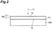
- FIG. 2 is a diagram explaining a cross-sectional configuration of a range image sensor.
- the range image sensor RS is a front-illuminated range image sensor, and includes a semiconductor substrate 1.
- the semiconductor substrate 1 has a first and a second surfaces 1a and 1b opposing each other.
- the second surface 1b is a light incident surface.
- the range image sensor RS is attached on the wiring substrate WB through an adhesive region FL in a state where a first surface 1a side of the semiconductor substrate 1 is opposing the wiring substrate WB.
- the adhesive region FL includes an insulation adhesive or a filler.
- the reflection light Lr is incident onto the range image sensor RS from a second surface 1b side of the semiconductor substrate 1.
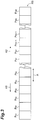
- FIG. 3 is a diagram illustrating a configuration of the range image sensor.
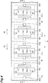
- FIG 4 is a substantially plan view illustrating the range image sensor.
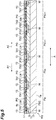
- FIG. 5 is a diagram illustrating a cross-sectional configuration taken along the line V-V of FIG. 4 .
- the range image sensor RS is a line sensor with an array structure that includes a plurality of range sensors P A1 to P AM , and P B1 to P BN (M and N are natural numbers equal to or greater than 2) disposed in a one-dimensional direction A.
- One, or two or more of the range sensors P A1 to P AM and P B1 to P BN constitute one pixel (channel) of the range image sensor RS.
- each of the range sensors P A1 to P AM and P B1 to P BN constitutes one pixel of the range image sensor RS.
- the range image sensor RS includes a light interception layer LI on the second surface 1b which is the light incident surface.
- an aperture LIa is formed in a region corresponding to each of the range sensors P A1 to P AM and P B1 to P BN in the one-dimensional direction A.
- the aperture LIa has a rectangular shape. In the present embodiment, the aperture LIa has an oblong rectangular shape.
- Light passes through the aperture LIa of the light interception layer LI, and is incident onto the semiconductor substrate 1.
- the aperture LIa defines a light receiving region in the semiconductor substrate 1.
- the light interception layer LI is made of, for example, metal, such as aluminum.
- the light interception layer LI is not illustrated in FIGS. 3 and 4 .
- the semiconductor substrate 1 includes a p-type first semiconductor region 3 positioned at the first surface 1a side, and a p - -type second semiconductor region 5 having a lower impurity concentration than the first semiconductor region 3 and positioned at the second surface 1b side.
- the semiconductor substrate 1 can be obtained by, for example, growing, on a p-type semiconductor substrate, a p - -type epitaxial layer having a lower impurity concentration than the semiconductor substrate.
- An insulation layer 7 is formed on the second surface 1b (the second semiconductor region 5) of the semiconductor substrate 1.
- the range sensors P A1 to P AM and P B1 to P BN are disposed on the semiconductor substrate 1 in the one-dimensional direction A. That is, the range sensors P A1 to P AM and P B1 to P BN are positioned in the semiconductor substrate 1 to be aligned along the one-dimensional direction A.
- each of the range sensors P A1 to P AM and P B1 to P BN includes a photo-gate electrode PG, a first and a second signal charge-accumulating regions FD1 and FD2, a first and a second transfer electrodes TX1 and TX2, and a p-type well region W.
- conductors 13 disposed on the first and second signal charge-accumulating regions FD1 and FD2 are omitted.
- each of the range sensors P A1 to P AM has a similar configuration to that of the range sensors P Am and P Am+1 .
- Each of the range sensors P B1 to P BN has a similar configuration to that of the range sensors P Bn and P Bn+1 .
- the photo-gate electrode PG is disposed corresponding to the aperture LIa.
- a region corresponding to the photo-gate electrode PG (a region located below the photo-gate electrode PG in FIG 5 ) in the semiconductor substrate 1 (the second semiconductor region 5) functions as a charge-generating region (a photosensitive region) that generates charges in accordance with incidence of the reflection light Lr of the pulse light Lp reflected off the object OJ.
- the photo-gate electrode PG also corresponds to the shape of the aperture LIa, and has a rectangular shape in a plan view. In the present embodiment, the photo-gate electrode PG has an oblong rectangular shape just like the aperture LIa.
- the photo-gate electrode PG has a planar shape having a first and a second long side-edges L1 and L2, which are orthogonal to the one-dimensional direction A and opposing each other, and a first and a second short side-edges S1 and S2, which are parallel to the one-dimensional direction A and opposing each other.
- the photo-gate electrode PG has the first long side-edge L1 in a side of one direction A1 of the one-dimensional direction A, and the second long side-edge L2 in a side of an another direction A2 of the one-dimensional direction A.
- the first and second signal charge-accumulating regions FD1 and FD2 are disposed to sandwich the photo-gate electrode PG in the one-dimensional direction A.
- the first signal charge-accumulating region FD1 is disposed at a first long side-edge L1 side of the photo-gate electrode PG away from the photo-gate electrode PG
- the second signal charge-accumulating region FD2 is disposed at a second long side-edge L2 side of the photo-gate electrode PG away from the photo-gate electrode PG
- the first signal charge-accumulating region FD1 is disposed at the second long side-edge L2 side of the photo-gate electrode PG separately from the photo-gate electrode PG.
- the second signal charge-accumulating region FD2 is disposed at the first long side-edge L1 side of the photo-gate electrode PG separately from the photo-gate electrode PG. That is, in any one of the range sensors P Am , P Am+1 , P Bn , and P Bn+1 , the first and second signal charge-accumulating regions FD1 and FD2 are disposed away from the charge-generating region (the region located below the photo-gate electrode PG).
- the first and second signal charge-accumulating regions FD1 and FD2 are n-type semiconductor regions, which are formed on the second semiconductor region 5 and have high impurity concentration, and accumulate charges generated in the charge-generating region as signal charges.
- the first and second signal charge-accumulating regions FD1 and FD2 each have a rectangular shape in a plan view.
- the first and second signal charge-accumulating regions FD1 and FD2 each have a square shape in a plan view, and have the same shape.
- the first and second signal charge-accumulating regions FD1 and FD2 are floating diffusion regions.
- the first transfer electrode TX1 is disposed on the insulation layer 7 and between the first signal charge-accumulating region FD1 and the photo-gate electrode PG.
- the first transfer electrode TX1 is disposed away from the first signal charge-accumulating region FD1 and the photo-gate electrode PG.
- the first transfer electrode TX1 allows the charges generated in the charge-generating region in accordance with the first transfer signal S p1 (see FIG. 8 ) to flow into the first signal charge-accumulating region FD1 as the signal charges.
- the second transfer electrode TX2 is disposed on the insulation layer 7 and between the second signal charge-accumulating region FD2 and the photo-gate electrode PG.
- the second transfer electrode TX2 is disposed away from the second signal charge-accumulating region FD2 and the photo-gate electrode PG.
- the second transfer electrode TX2 allows the charges generated in the charge-generating region in accordance with the second transfer signal S p2 (see FIG. 8 ), which is different in phase from the first transfer signal S p1 , to flow into the second signal charge-accumulating region FD2 as the signal charges.
- the first and second transfer electrodes TX1 and TX2 each have a rectangular shape in a plan view.
- the first and second transfer electrodes TX1 and TX2 each have an oblong rectangular shape having long side-edges in the direction orthogonal to the one-dimensional direction A, and have the same shape.
- the length of the long side-edges of the first and second transfer electrodes TX1 and TX2 is shorter than the length of the first and second long side-edges L1 and L2 of the photo-gate electrode PG.
- the first signal charge-accumulating regions FD1 are adjacent to each other in the one-dimensional direction A.
- the second signal charge-accumulating regions FD2 are adjacent to each other in the one-dimensional direction A.
- the first signal charge-accumulating region FD1 and the second signal charge-accumulating region FD2 are adjacent to each other in the one-dimensional direction A.
- the first signal charge-accumulating region FD1 and the second signal charge-accumulating region FD2 are adjacent to each other in the one-dimensional direction A.
- the first signal charge-accumulating regions FD1 are adjacent to each other in the one-dimensional direction A in a range sensor (for example, the range sensor P Am ) positioned in a center of the three range sensors and a range sensor (for example, the range sensor P Bn ) positioned next to the range sensor in one direction A1.
- the first signal charge-accumulating region FD1 and the second signal charge-accumulating region FD2 are adjacent to each other in the one-dimensional direction A.
- the second signal charge-accumulating regions FD2 are adjacent to each other in the one-dimensional direction A in the range sensor P Am+1 positioned in a center of the three range sensors P Am , P Am+1 , P Bn+1 and the range sensor P Bn+1 positioned next to the range sensor P Am+1 in the other direction A2.
- the first signal charge-accumulating region FD1 and the second signal charge-accumulating region FD2 are adjacent to each other in the one-dimensional direction A.
- the range image sensor RS includes a plurality of first range sensor groups including the two range sensors P Am and P Bn in which the first signal charge-accumulating regions FD1 are adjacent to each other in the one-dimensional direction A, and a plurality of second range sensor groups including the two range sensors P Am+1 and P Bn+1 in which the second signal charge-accumulating regions FD2 are adjacent to each other in the one-dimensional direction A.
- the plurality of first range sensor groups and the plurality of second range sensor groups are alternately aligned in the one-dimensional direction A.
- the first transfer electrodes TX1 are adjacent to each other in the one-dimensional direction A.
- the second transfer electrodes TX2 are adjacent to each other in the one-dimensional direction A.
- the first transfer electrode TX1 and the second transfer electrode TX2 are adjacent to each other in the one-dimensional direction A.
- the first transfer electrode TX1 and the second transfer electrode TX2 are adjacent to each other in the one-dimensional direction A.
- the first transfer electrode TX1 and the second transfer electrode TX2 are adjacent to each other in the one-dimensional direction A.
- the well region W is formed in the second semiconductor region 5 to surround the photo-gate electrode PG, the first and second transfer electrodes TX1 and TX2, and the first and second signal charge-accumulating regions FD1 and FD2 when viewed from the direction orthogonal to the second surface 1b.
- the well region W is overlapped by a portion of each of the first and second signal charge-accumulating regions FD1 and FD2 when viewed from the direction orthogonal to the second surface 1b.
- a periphery of the well region W substantially conforms to a periphery of each of the range sensors P A1 to P AM and P B1 to P BN .
- the well region W is the same conductive type as the conductive type of the second semiconductor region 5, and has higher impurity concentration than the impurity concentration of the second semiconductor region 5.
- the well region W suppresses the coupling between a depletion layer expanded by applying voltage to the photo-gate electrode PG and a depletion layer expanded from the first and second signal charge-accumulating regions FD1 and FD2. Accordingly, a crosstalk is suppressed.
- the insulation layer 7 is provided with contact holes for exposing the surface of the second semiconductor region 5.
- the conductors 13 are disposed in the contact holes to connect the first and second signal charge-accumulating regions FD1 and FD2 to the outside thereof.
- the "high impurity concentration” means that impurity concentration is, for example, about 1 ⁇ 10 17 cm -3 or more, and is indicated by adding "+” to a conductive type.
- the "low impurity concentration” means that impurity concentration is, for example, about 10 ⁇ 10 15 cm -3 or less, and is indicated by adding "-" to a conductive type.
- the thickness/impurity concentration of each semiconductor region is as follows:
- a reference potential (for example, a ground potential) is supplied to the semiconductor substrate 1 (the first and second semiconductor regions 3 and 5) through a back gate, a through-via electrode, or the like.
- the semiconductor substrate 1 is made of Si
- the insulation layer 7 is made of SiO 2
- the photo-gate electrode PG and the first and second transfer electrodes TX1 and TX2 are made of polysilicon, but they may be made of other materials.
- the phase of the first transfer signal S p1 applied to the first transfer electrode TX1 is shifted by 180° from the phase of the second transfer signal S p2 applied to the second transfer electrode TX2.
- the light incident on the range sensors P A1 to P AM and P B1 to P BN is converted into charges in the semiconductor substrate 1 (the second semiconductor region 5).
- a part of the generated charges moves, as the signal charges, in a direction of the first transfer electrode TX1 or the second transfer electrode TX2 in accordance with a potential gradient formed by voltage applied to the photo-gate electrode PG and the first and second transfer electrodes TX1 and TX2. That is, a part of the generated charges moves, as the signal charges, in a direction parallel to the first and second short side-edges S1 and S2 of the photo-gate electrode PG.
- a potential below the first transfer electrode TX1 becomes lower than a potential in the region below the photo-gate electrode PG in the semiconductor substrate 1 (the second semiconductor region 5) with respect to a negative charge (electrons).
- the electrons are drawn in the direction of the first transfer electrode TX1, and accumulated in a potential well formed by the first signal charge-accumulating region FD1.
- a potential below the second transfer electrode TX2 becomes lower than a potential in the region below the photo-gate electrode PG in the semiconductor substrate 1 (the second semiconductor region 5) with respect to a negative charge (electron).
- the electron is drawn in the direction of the second transfer electrode TX2, and accumulated in a potential well formed by the second signal charge-accumulating region FD2.
- An n-type semiconductor contains a positively ionized donor, has a positive potential, and attracts electrons.
- a potential for example, a ground potential
- a potential barrier is generated by the first or second transfer electrode TX1 or TX2.
- FIGS. 6 and 7 are diagrams illustrating potential profiles in the vicinity of the second surface of the semiconductor substrate taken along the line V-V of FIG. 4 .
- the downward direction is the positive direction of a potential.
- a potential ⁇ PG in the region immediately below the photo-gate electrode PG is set slightly higher than a substrate potential due to a potential supplied to the photo-gate electrode PG (for example, an intermediate potential between a higher electric potential and a lower electric potential supplied to the first transfer electrode TX1).
- a potential ⁇ TX1 in the region immediately below the first transfer electrode TX1, a potential ⁇ TX2 in the region immediately below the second transfer electrode TX2, a potential ⁇ PG in the charge-generating region immediately below the photo-gate electrode PG, a potential ⁇ FD1 in the first signal charge-accumulating region FD1, and a potential ⁇ FD2 in the second signal charge-accumulating region FD2 are illustrated.
- the potential ⁇ TX2 in the semiconductor region immediately below the second transfer electrode TX2 does not become lower, and the charge does not flow into the potential well of the second signal charge-accumulating region FD2. Therefore, the signal charges are collected and accumulated in the potential well of the first signal charge-accumulating region FD1. Since the first and second signal charge-accumulating regions FD1 and FD2 are doped with n-type impurities, and the potentials are recessed in the positive direction.
- a positive potential is supplied to the second transfer electrode TX2.
- An inverse potential that is, a potential whose phase is shifted by 180° (for example, a ground potential) is supplied to the first transfer electrode TX1.
- An intermediate potential between the potential supplied to the first transfer electrode TX1 and the potential supplied to the second transfer electrode TX2 is supplied to the photo-gate electrode PG.
- the potential ⁇ TX2 in the semiconductor region immediately below the second transfer electrode TX2 becomes lower than the potential ⁇ PG in the charge-generating region as illustrated in FIG. 7 , and thus negative charge e generated in the charge-generating region flows into the potential well of the second signal charge-accumulating region FD2.
- the potential ⁇ TX1 in the semiconductor region immediately below the first transfer electrode TX1 does not become lower, and the charge does not flow into the potential well of the first signal charge-accumulating region FD1. Therefore, the signal charges are collected and accumulated in the potential well of the second signal charge-accumulating region FD2.
- the signal charges are collected and accumulated in the potential wells of the first and second signal charge-accumulating regions FD1 and FD2.
- the signal charges accumulated in the potential wells of the first and second signal charge-accumulating regions FD1 and FD2 are read out to the outside thereof.
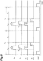
- FIG. 8 is a timing chart of various signals.
- FIG. 8 illustrates various signals in two frame periods T F , which are continuous in time series, among a plurality of frame periods T F .
- a drive signal S D of the light source LS an intensity signal S Lr of the reflection light Lr, a first transfer signal S p1 applied to the first transfer electrode TX1, a second transfer signal S p2 applied to the second transfer electrode TX2, and a reset signal reset are illustrated.
- the intensity signal S Lr of the reflection light Lr is an intensity signal obtained by causing the reflection light Lr of the pulse light Lp at the object OJ to be incident onto the range image sensor RS (the charge-generating region).
- the two frame periods T F each include a period in which the signal charges are accumulated (an accumulation period) T acc and a period in which the signal charges are read out (a readout period) T ro . All of the drive signal S D , the intensity signal S Lr , the first transfer signal S p1 , and the second transfer signal S p2 are pulse signals having the pulse width T p .
- the reset signal reset is applied to the first and second signal charge-accumulating regions FD1 and FD2. Accordingly, the charges accumulated in the first and second signal charge-accumulating regions FD1 and FD2 are discharged to the outside thereof.
- the reset signal reset turns momentarily ON and then turned OFF, the drive signal S D is applied to the light source LS thereafter.
- the first and second transfer signals S p1 and S p2 are applied to the first and second transfer electrodes TX1 and TX2 in an inverse phase to each other.
- the charges are transferred, and the signal charges are accumulated in the first and second signal charge-accumulating regions FD1 and FD2. Then, during the readout period T r0 , the signal charges accumulated in the first and second signal charge-accumulating regions FD1 and FD2 are read out.
- the first transfer signal S p1 is output in synchronization with the drive signal S D at the phase difference 0
- the second transfer signal S p2 is output in synchronization with the drive signal S D at the phase difference 180°.
- the output of the first and second transfer signals S p1 and S p2 is controlled by the controlling unit CONT.
- the controlling unit CONT outputs the first transfer signal S p1 to the first transfer electrode TX1 so that the charges generated in the charge-generating region flow into the first signal charge-accumulating region FD1 as the signal charges and outputs the second transfer signal S p2 different in phase from the first transfer signal S p1 to the second transfer electrode TX2 so that the charges generated in the charge-generating region flow into the second signal charge-accumulating region FD2 as the signal charges, to synchronize with the emission of the pulse light Lp.
- the charge quantity q 1 corresponds to an overlap between the intensity signal S Lr and the first transfer signal S p1 output in synchronization with the drive signal S D at the phase difference 0 is accumulated in the first signal charge-accumulating region FD1.
- the charge quantity q 2 corresponds to an overlap between the intensity signal S Lr of the reflection light Lr and the second transfer signal S p2 output in synchronization with the drive signal S D at the phase difference 180° is accumulated in the second signal charge-accumulating region FD2.
- the phase difference Td between the intensity signal S Lr and the signal output in synchronization with the drive signal S D at the phase difference 0 is equal to the flight time of the light, and indicates the distance d from the range image sensor RS to the object OJ.
- the distance d is calculated by the arithmetic unit ART using a ratio of the charge quantity q 1 and the charge quantity q 2 in one frame period T F with the following expression (1).
- c is the speed of light.
- Distance d c / 2 ⁇ T P ⁇ q 2 / q 1 + q 2
- the arithmetic unit ART reads out the charge quantity q 1 and q 2 of the signal charges accumulated in the first and second signal charge-accumulating regions FD1 and FD2 per each frame period T F , and calculates the distance d to the object OJ based on the readout charge quantities q 1 and q 2 .
- a charge-distributing type range image sensor including a plurality of range sensors disposed in a one-dimensional direction
- charge crosstalk leakage
- the influence of the charge crosstalk on ranging can be different between the adjacent range sensors. If the influence of the charge crosstalk on the ranging is different between the adjacent range sensors, it is difficult to appropriately perform the ranging.
- each of the range sensors includes, for example, the first signal charge-accumulating region and the first transfer electrode closer to one side of the one-dimensional direction than the photo-gate electrode, and includes the second signal charge-accumulating region and the second transfer electrode closer to an another side of the one-dimensional direction than the photo-gate electrode.
- the first signal charge-accumulating region and the second signal charge-accumulating region are adjacent to each other in the one-dimensional direction.
- the range sensor when reflection light is incident into, for example, the range sensor positioned in the center of the three range sensors, charges are generated in the range sensor (hereinafter, referred to as an incident range sensor) in accordance with the reflection light.
- the generated charges are distributed to the first and second signal charge-accumulating regions of the incident range sensor in accordance with the first and second transfer signals.
- a part of the charges leaks into the first and second signal charge-accumulating regions of the two range sensors other than the incident range sensor.
- the leakage quantity largely varies depending on whether the first and second signal charge-accumulating regions are disposed at the incident range sensor side.
- the first signal charge-accumulating region is disposed closer to the incident range sensor side than the charge-generating region, and the second signal charge-accumulating region is disposed closer to the opposite side to the incident range sensor than the charge-generating region.
- the second signal charge-accumulating region is disposed closer to the incident range sensor side than the charge-generating region, and the first signal charge-accumulating region is disposed closer to the opposite side to the incident range sensor than the charge-generating region.
- the leakage quantity to the first signal charge-accumulating region is larger than the leakage quantity to the second signal charge-accumulating region in the one-side range sensor.
- the leakage quantity to the second signal charge-accumulating region is larger than the leakage quantity to the first signal charge-accumulating region in the other-side range sensor.
- a range sensor positioned next to the arbitrary range sensor in the one direction A1 in a case where the first signal charge-accumulating region FD1 is positioned closer to the other direction A2 side than the charge-generating region, the first signal charge-accumulating region FD1 is positioned closer to the one direction A1 side than the charge-generating region in a range sensor positioned next to the arbitrary range sensor in the other direction A2.
- the second signal charge-accumulating region FD2 is positioned closer to the other direction A2 side than the charge-generating region, the second signal charge-accumulating region FD2 is positioned closer to the one direction A1 side than the charge-generating region in the range sensor positioned next to the arbitrary range sensor in the other direction A2.
- the signal charge-accumulating regions positioned at the arbitrary range sensor side are the first signal charge-accumulating regions FD1 or the second signal charge-accumulating regions FD2, and the same types of signal charge-accumulating regions.
- the leaking charges flow into the first signal charge-accumulating regions FD1 or the second signal charge-accumulating regions FD2 of two range sensors.
- the charges leaking into the above two range sensors are accumulated in the first signal charge-accumulating regions FD1 or the second signal charge-accumulating regions FD2 of the two range sensors.
- the types of the signal charge-accumulating regions, in which the leaking charges are accumulated are the same in the two range sensors positioned at both sides among any three of three range sensors consecutively aligned in the one-dimensional direction A. For this reason, and the influence of the charge crosstalk on ranging between the range sensors adjacent to each other in the one-dimensional direction A is similar.
- the range sensors P A1 to P AM and P B1 to P BN each include one first transfer electrode TX1, one second transfer electrode TX2, one first signal charge-accumulating region FD1, and one second signal charge-accumulating region FD2, but are not limited thereto.
- the range sensors P A1 to P AM and P B1 to P BN each may include two or more first transfer electrodes TX1, two or more second transfer electrodes TX2, two or more first signal charge-accumulating regions FD1, and two or more second signal charge-accumulating regions FD2.
- the range sensors P A1 to P AM and P B1 to P BN each may further include an unnecessary charge-discharging region and a third transfer electrode.
- the unnecessary charge-discharging region discharges the charges generated in the charge-generating region to the outside thereof as unnecessary charges.
- the third transfer electrode is disposed between the unnecessary charge-discharging region and the charge-generating region, and allows the charges generated in the charge-generating region into the unnecessary charge-discharging region as the unnecessary charges in accordance with a third transfer signal different in phase from the first and second transfer signals.
- the unnecessary charges can be discharged to the outside thereof, and it is possible to improve ranging accuracy.
- the unnecessary charge-discharging region and the third transfer electrode each may be two or more.
- the drive signals S D are successively applied, and in synchronization with which, the first transfer signal S p1 and the second transfer signal S p2 may be successively output.
- the signal charges are integrated and accumulated in the first and second signal charge-accumulating regions FD1 and FD2.
- the range image sensor RS is the line sensor that includes the plurality of range sensors P A1 to P AM and P B1 to P BN disposed one-dimensionally
- the range sensors P A1 to P AM and P B1 to P BN may be disposed two-dimensionally. In this case, a two-dimensional image can be easily obtained.
- a two-dimensional image can be obtained by rotating the line sensor or by scanning with two line sensors.
- the range image sensor RS is not limited to the front-illuminated range image sensor.
- the range image sensor RS may be a back-illuminated range image sensor.
- the charge-generating region that generates the charges in accordance with incident light may include a photodiode (for example, an embedded photodiode).
- the p-type and n-type of conductive types in the range image sensor RS according to the present embodiment may be replaced by each other to be inversed to those in the above description.
- the present invention can be applicable to a charge-distributing type range image sensor.
- ranging device A: one-dimensional direction
- FD1 first signal charge-accumulating region
- FD2 second signal charge-accumulating region
- PG photo-gate electrode
- RS range image sensor
- S p1 first transfer signal
- S p2 second transfer signal
- TX1 first transfer electrode
- TX2 second transfer electrode.
Landscapes
- Engineering & Computer Science (AREA)
- Physics & Mathematics (AREA)
- General Physics & Mathematics (AREA)
- Radar, Positioning & Navigation (AREA)
- Remote Sensing (AREA)
- Computer Networks & Wireless Communication (AREA)
- Electromagnetism (AREA)
- Solid State Image Pick-Up Elements (AREA)
- Measurement Of Optical Distance (AREA)
- Optical Radar Systems And Details Thereof (AREA)
Claims (1)
- Entfernungsbildsensor, umfassend eine Vielzahl von Entfernungssensoren (PA1 bis PAM; PB1 bis PBM), angeordnet in einer eindimensionalen Richtung (A), wobei jeder der Vielzahl von Entfernungssensoren umfasst:einen Ladungserzeugungsbereich, der Ladungen gemäß einfallendem Licht erzeugt;einen ersten und einen zweiten Signalladungsakkumulationsbereich (FD1, FD2), entfernt angeordnet von dem Ladungserzeugungsbereich, um den Ladungserzeugungsbereich in der eindimensionalen Richtung einzuschließen und die in dem Ladungserzeugungsbereich erzeugten Ladungen als Signalladungen zu akkumulieren;eine erste Übertragungselektrode (TX1), angeordnet zwischen dem ersten Signalladungsakkumulationsbereich (FD1) und dem Ladungserzeugungsbereich und konfiguriert zum Zulassen, dass die Ladungen, die in dem Ladungserzeugungsbereich erzeugt wurden, in den ersten Signalladungsakkumulationsbereich fließen, während das Signal gemäß einem ersten Übertragungssignal lädt; undeine zweite Übertragungselektrode (TX2), angeordnet zwischen dem zweiten Signalladungsakkumulationsbereich (FD2) und dem Ladungserzeugungsbereich und konfiguriert zum Zulassen, dass die Ladungen, die in dem Ladungserzeugungsbereich erzeugt wurden, in den zweiten Signalladungsakkumulationsbereich fließen, während das Signal gemäß einem zweiten Übertragungssignal lädt, das eine andere Phase als das erste Übertragungssignal aufweist,dadurch gekennzeichnet, dassin drei beliebigen der Entfernungssensoren, die nacheinander in der eindimensionalen Richtung ausgerichtet sind, zwei erste Signalladungsakkumulationsbereiche unterschiedlicher Entfernungssensoren oder zwei zweite Signalladungsakkumulationsbereiche unterschiedlicher Entfernungssensoren in der eindimensionalen Richtung einander benachbart sind in einem Entfernungssensor, der in einer Mitte der drei Entfernungssensoren positioniert ist, und einem Entfernungssensor, der näher an einer Seite der eindimensionalen Richtung angeordnet ist als der Entfernungssensor, der in der Mitte der drei Entfernungssensoren positioniert ist, und zwei erste Signalladungsakkumulationsbereich und der zweite Signalladungsakkumulationsbereich unterschiedlicher Entfernungssensoren in der eindimensionalen Richtung einander benachbart sind in dem Entfernungssensor, der in einer Mitte der drei Entfernungssensoren positioniert ist, und einem Entfernungssensor, der näher an einer anderen Seite der eindimensionalen Richtung angeordnet ist als der Entfernungssensor, der in der Mitte der drei Entfernungssensoren positioniert ist.
Applications Claiming Priority (2)
| Application Number | Priority Date | Filing Date | Title |
|---|---|---|---|
| JP2014096703A JP6386777B2 (ja) | 2014-05-08 | 2014-05-08 | 距離画像センサ |
| PCT/JP2015/052465 WO2015170487A1 (ja) | 2014-05-08 | 2015-01-29 | 距離画像センサ |
Publications (3)
| Publication Number | Publication Date |
|---|---|
| EP3141927A1 EP3141927A1 (de) | 2017-03-15 |
| EP3141927A4 EP3141927A4 (de) | 2018-03-28 |
| EP3141927B1 true EP3141927B1 (de) | 2019-04-03 |
Family
ID=54392342
Family Applications (1)
| Application Number | Title | Priority Date | Filing Date |
|---|---|---|---|
| EP15789629.1A Active EP3141927B1 (de) | 2014-05-08 | 2015-01-29 | Abstandsbildsensor |
Country Status (6)
| Country | Link |
|---|---|
| US (1) | US10224354B2 (de) |
| EP (1) | EP3141927B1 (de) |
| JP (1) | JP6386777B2 (de) |
| KR (1) | KR102216698B1 (de) |
| CN (1) | CN106461761B (de) |
| WO (1) | WO2015170487A1 (de) |
Families Citing this family (8)
| Publication number | Priority date | Publication date | Assignee | Title |
|---|---|---|---|---|
| JP6659447B2 (ja) | 2016-05-02 | 2020-03-04 | 浜松ホトニクス株式会社 | 距離センサ |
| JP6659448B2 (ja) * | 2016-05-02 | 2020-03-04 | 浜松ホトニクス株式会社 | 距離センサ及び距離センサの駆動方法 |
| CN115137336A (zh) | 2017-02-28 | 2022-10-04 | 松下知识产权经营株式会社 | 处理方法、系统及存储介质 |
| JP7045639B2 (ja) * | 2017-02-28 | 2022-04-01 | パナソニックIpマネジメント株式会社 | 作業適正度判定システム |
| US11221402B2 (en) * | 2017-12-31 | 2022-01-11 | NewSight Imaging Ltd. | Active pixel array for a time of flight detector |
| US10892295B2 (en) | 2018-01-10 | 2021-01-12 | Microsoft Technology Licensing, Llc | Germanium-modified, back-side illuminated optical sensor |
| KR102615195B1 (ko) | 2018-07-19 | 2023-12-18 | 삼성전자주식회사 | ToF 기반의 3D 이미지 센서 및 그 이미지 센서를 구비한 전자 장치 |
| JP7172963B2 (ja) * | 2018-12-14 | 2022-11-16 | 株式会社デンソー | 光学的測距装置、レーザ発光装置の製造方法 |
Family Cites Families (17)
| Publication number | Priority date | Publication date | Assignee | Title |
|---|---|---|---|---|
| JPS63177460A (ja) * | 1987-01-16 | 1988-07-21 | Sony Corp | 固体撮像装置 |
| EP1356664A4 (de) * | 2000-12-11 | 2009-07-22 | Canesta Inc | Cmos-kompatible dreidimensionale bilderfassung durch quanteneffizienzmodulation |
| JP4280822B2 (ja) * | 2004-02-18 | 2009-06-17 | 国立大学法人静岡大学 | 光飛行時間型距離センサ |
| CN100394609C (zh) * | 2004-09-07 | 2008-06-11 | 三洋电机株式会社 | 固体摄像装置 |
| US7781811B2 (en) * | 2005-08-30 | 2010-08-24 | National University Corporation Shizuoka University | Semiconductor range-finding element and solid-state imaging device |
| WO2007119626A1 (ja) * | 2006-03-31 | 2007-10-25 | National University Corporation Shizuoka University | 半導体測距素子及び固体撮像装置 |
| JP2009047661A (ja) * | 2007-08-22 | 2009-03-05 | Hamamatsu Photonics Kk | 測距装置 |
| JP5483689B2 (ja) * | 2009-11-24 | 2014-05-07 | 浜松ホトニクス株式会社 | 距離センサ及び距離画像センサ |
| JP5558999B2 (ja) * | 2009-11-24 | 2014-07-23 | 浜松ホトニクス株式会社 | 距離センサ及び距離画像センサ |
| JP5244076B2 (ja) * | 2009-11-24 | 2013-07-24 | 浜松ホトニクス株式会社 | 距離センサ及び距離画像センサ |
| JP5620087B2 (ja) * | 2009-11-30 | 2014-11-05 | 浜松ホトニクス株式会社 | 距離センサ及び距離画像センサ |
| JP2012083214A (ja) * | 2010-10-12 | 2012-04-26 | Hamamatsu Photonics Kk | 距離センサ及び距離画像センサ |
| JP2012083213A (ja) * | 2010-10-12 | 2012-04-26 | Hamamatsu Photonics Kk | 距離センサ及び距離画像センサ |
| JP5518667B2 (ja) * | 2010-10-12 | 2014-06-11 | 浜松ホトニクス株式会社 | 距離センサ及び距離画像センサ |
| JP5502694B2 (ja) * | 2010-10-12 | 2014-05-28 | 浜松ホトニクス株式会社 | 距離センサ及び距離画像センサ |
| JP6026755B2 (ja) * | 2012-02-28 | 2016-11-16 | 浜松ホトニクス株式会社 | 距離センサ及び距離画像センサ |
| US9134401B2 (en) * | 2012-03-27 | 2015-09-15 | Hamamatsu Photonics K. K. | Range sensor and range image sensor |
-
2014
- 2014-05-08 JP JP2014096703A patent/JP6386777B2/ja active Active
-
2015
- 2015-01-29 KR KR1020167033867A patent/KR102216698B1/ko active Active
- 2015-01-29 US US15/308,668 patent/US10224354B2/en active Active
- 2015-01-29 CN CN201580023670.8A patent/CN106461761B/zh active Active
- 2015-01-29 EP EP15789629.1A patent/EP3141927B1/de active Active
- 2015-01-29 WO PCT/JP2015/052465 patent/WO2015170487A1/ja not_active Ceased
Non-Patent Citations (1)
| Title |
|---|
| None * |
Also Published As
| Publication number | Publication date |
|---|---|
| KR102216698B1 (ko) | 2021-02-17 |
| CN106461761B (zh) | 2020-03-27 |
| JP2015215182A (ja) | 2015-12-03 |
| JP6386777B2 (ja) | 2018-09-05 |
| EP3141927A1 (de) | 2017-03-15 |
| EP3141927A4 (de) | 2018-03-28 |
| KR20170002544A (ko) | 2017-01-06 |
| US10224354B2 (en) | 2019-03-05 |
| WO2015170487A1 (ja) | 2015-11-12 |
| CN106461761A (zh) | 2017-02-22 |
| US20170194370A1 (en) | 2017-07-06 |
Similar Documents
| Publication | Publication Date | Title |
|---|---|---|
| EP3141927B1 (de) | Abstandsbildsensor | |
| EP3141930B1 (de) | Distanzmessvorrichtung und verfahren zur stromversorgung einer distanzmessvorrichtung | |
| EP2506036B1 (de) | Bereichssensor und bereichsbildsensor | |
| CN103155150B (zh) | 距离传感器以及距离图像传感器 | |
| US11054522B2 (en) | Distance measuring device | |
| EP3506355B1 (de) | Abstandssensor und abstandsbildsensor | |
| US10436908B2 (en) | Range image sensor | |
| EP2821812B1 (de) | Bereichssensor und bereichsbildsensor | |
| US9664780B2 (en) | Distance sensor and distance image sensor | |
| JP5502694B2 (ja) | 距離センサ及び距離画像センサ | |
| JP2012083222A (ja) | 距離センサ及び距離画像センサ |
Legal Events
| Date | Code | Title | Description |
|---|---|---|---|
| STAA | Information on the status of an ep patent application or granted ep patent |
Free format text: STATUS: THE INTERNATIONAL PUBLICATION HAS BEEN MADE |
|
| PUAI | Public reference made under article 153(3) epc to a published international application that has entered the european phase |
Free format text: ORIGINAL CODE: 0009012 |
|
| STAA | Information on the status of an ep patent application or granted ep patent |
Free format text: STATUS: REQUEST FOR EXAMINATION WAS MADE |
|
| 17P | Request for examination filed |
Effective date: 20161019 |
|
| AK | Designated contracting states |
Kind code of ref document: A1 Designated state(s): AL AT BE BG CH CY CZ DE DK EE ES FI FR GB GR HR HU IE IS IT LI LT LU LV MC MK MT NL NO PL PT RO RS SE SI SK SM TR |
|
| AX | Request for extension of the european patent |
Extension state: BA ME |
|
| DAX | Request for extension of the european patent (deleted) | ||
| A4 | Supplementary search report drawn up and despatched |
Effective date: 20180227 |
|
| RIC1 | Information provided on ipc code assigned before grant |
Ipc: H01L 27/146 20060101ALI20180221BHEP Ipc: G01S 7/486 20060101AFI20180221BHEP Ipc: G01S 17/89 20060101ALI20180221BHEP |
|
| GRAP | Despatch of communication of intention to grant a patent |
Free format text: ORIGINAL CODE: EPIDOSNIGR1 |
|
| STAA | Information on the status of an ep patent application or granted ep patent |
Free format text: STATUS: GRANT OF PATENT IS INTENDED |
|
| INTG | Intention to grant announced |
Effective date: 20181116 |
|
| GRAS | Grant fee paid |
Free format text: ORIGINAL CODE: EPIDOSNIGR3 |
|
| GRAA | (expected) grant |
Free format text: ORIGINAL CODE: 0009210 |
|
| STAA | Information on the status of an ep patent application or granted ep patent |
Free format text: STATUS: THE PATENT HAS BEEN GRANTED |
|
| AK | Designated contracting states |
Kind code of ref document: B1 Designated state(s): AL AT BE BG CH CY CZ DE DK EE ES FI FR GB GR HR HU IE IS IT LI LT LU LV MC MK MT NL NO PL PT RO RS SE SI SK SM TR |
|
| REG | Reference to a national code |
Ref country code: GB Ref legal event code: FG4D |
|
| REG | Reference to a national code |
Ref country code: CH Ref legal event code: EP Ref country code: AT Ref legal event code: REF Ref document number: 1116401 Country of ref document: AT Kind code of ref document: T Effective date: 20190415 |
|
| REG | Reference to a national code |
Ref country code: DE Ref legal event code: R096 Ref document number: 602015027687 Country of ref document: DE |
|
| REG | Reference to a national code |
Ref country code: IE Ref legal event code: FG4D |
|
| REG | Reference to a national code |
Ref country code: CH Ref legal event code: NV Representative=s name: SERVOPATENT GMBH, CH |
|
| REG | Reference to a national code |
Ref country code: NL Ref legal event code: MP Effective date: 20190403 |
|
| REG | Reference to a national code |
Ref country code: LT Ref legal event code: MG4D |
|
| REG | Reference to a national code |
Ref country code: AT Ref legal event code: MK05 Ref document number: 1116401 Country of ref document: AT Kind code of ref document: T Effective date: 20190403 |
|
| PG25 | Lapsed in a contracting state [announced via postgrant information from national office to epo] |
Ref country code: NL Free format text: LAPSE BECAUSE OF FAILURE TO SUBMIT A TRANSLATION OF THE DESCRIPTION OR TO PAY THE FEE WITHIN THE PRESCRIBED TIME-LIMIT Effective date: 20190403 |
|
| PG25 | Lapsed in a contracting state [announced via postgrant information from national office to epo] |
Ref country code: CZ Free format text: LAPSE BECAUSE OF FAILURE TO SUBMIT A TRANSLATION OF THE DESCRIPTION OR TO PAY THE FEE WITHIN THE PRESCRIBED TIME-LIMIT Effective date: 20190403 Ref country code: NO Free format text: LAPSE BECAUSE OF FAILURE TO SUBMIT A TRANSLATION OF THE DESCRIPTION OR TO PAY THE FEE WITHIN THE PRESCRIBED TIME-LIMIT Effective date: 20190703 Ref country code: PT Free format text: LAPSE BECAUSE OF FAILURE TO SUBMIT A TRANSLATION OF THE DESCRIPTION OR TO PAY THE FEE WITHIN THE PRESCRIBED TIME-LIMIT Effective date: 20190803 Ref country code: FI Free format text: LAPSE BECAUSE OF FAILURE TO SUBMIT A TRANSLATION OF THE DESCRIPTION OR TO PAY THE FEE WITHIN THE PRESCRIBED TIME-LIMIT Effective date: 20190403 Ref country code: SE Free format text: LAPSE BECAUSE OF FAILURE TO SUBMIT A TRANSLATION OF THE DESCRIPTION OR TO PAY THE FEE WITHIN THE PRESCRIBED TIME-LIMIT Effective date: 20190403 Ref country code: AL Free format text: LAPSE BECAUSE OF FAILURE TO SUBMIT A TRANSLATION OF THE DESCRIPTION OR TO PAY THE FEE WITHIN THE PRESCRIBED TIME-LIMIT Effective date: 20190403 Ref country code: HR Free format text: LAPSE BECAUSE OF FAILURE TO SUBMIT A TRANSLATION OF THE DESCRIPTION OR TO PAY THE FEE WITHIN THE PRESCRIBED TIME-LIMIT Effective date: 20190403 Ref country code: ES Free format text: LAPSE BECAUSE OF FAILURE TO SUBMIT A TRANSLATION OF THE DESCRIPTION OR TO PAY THE FEE WITHIN THE PRESCRIBED TIME-LIMIT Effective date: 20190403 Ref country code: LT Free format text: LAPSE BECAUSE OF FAILURE TO SUBMIT A TRANSLATION OF THE DESCRIPTION OR TO PAY THE FEE WITHIN THE PRESCRIBED TIME-LIMIT Effective date: 20190403 |
|
| PG25 | Lapsed in a contracting state [announced via postgrant information from national office to epo] |
Ref country code: LV Free format text: LAPSE BECAUSE OF FAILURE TO SUBMIT A TRANSLATION OF THE DESCRIPTION OR TO PAY THE FEE WITHIN THE PRESCRIBED TIME-LIMIT Effective date: 20190403 Ref country code: RS Free format text: LAPSE BECAUSE OF FAILURE TO SUBMIT A TRANSLATION OF THE DESCRIPTION OR TO PAY THE FEE WITHIN THE PRESCRIBED TIME-LIMIT Effective date: 20190403 Ref country code: BG Free format text: LAPSE BECAUSE OF FAILURE TO SUBMIT A TRANSLATION OF THE DESCRIPTION OR TO PAY THE FEE WITHIN THE PRESCRIBED TIME-LIMIT Effective date: 20190703 Ref country code: PL Free format text: LAPSE BECAUSE OF FAILURE TO SUBMIT A TRANSLATION OF THE DESCRIPTION OR TO PAY THE FEE WITHIN THE PRESCRIBED TIME-LIMIT Effective date: 20190403 Ref country code: GR Free format text: LAPSE BECAUSE OF FAILURE TO SUBMIT A TRANSLATION OF THE DESCRIPTION OR TO PAY THE FEE WITHIN THE PRESCRIBED TIME-LIMIT Effective date: 20190704 |
|
| PG25 | Lapsed in a contracting state [announced via postgrant information from national office to epo] |
Ref country code: IS Free format text: LAPSE BECAUSE OF FAILURE TO SUBMIT A TRANSLATION OF THE DESCRIPTION OR TO PAY THE FEE WITHIN THE PRESCRIBED TIME-LIMIT Effective date: 20190803 Ref country code: AT Free format text: LAPSE BECAUSE OF FAILURE TO SUBMIT A TRANSLATION OF THE DESCRIPTION OR TO PAY THE FEE WITHIN THE PRESCRIBED TIME-LIMIT Effective date: 20190403 |
|
| REG | Reference to a national code |
Ref country code: DE Ref legal event code: R097 Ref document number: 602015027687 Country of ref document: DE |
|
| PG25 | Lapsed in a contracting state [announced via postgrant information from national office to epo] |
Ref country code: RO Free format text: LAPSE BECAUSE OF FAILURE TO SUBMIT A TRANSLATION OF THE DESCRIPTION OR TO PAY THE FEE WITHIN THE PRESCRIBED TIME-LIMIT Effective date: 20190403 Ref country code: SK Free format text: LAPSE BECAUSE OF FAILURE TO SUBMIT A TRANSLATION OF THE DESCRIPTION OR TO PAY THE FEE WITHIN THE PRESCRIBED TIME-LIMIT Effective date: 20190403 Ref country code: DK Free format text: LAPSE BECAUSE OF FAILURE TO SUBMIT A TRANSLATION OF THE DESCRIPTION OR TO PAY THE FEE WITHIN THE PRESCRIBED TIME-LIMIT Effective date: 20190403 Ref country code: EE Free format text: LAPSE BECAUSE OF FAILURE TO SUBMIT A TRANSLATION OF THE DESCRIPTION OR TO PAY THE FEE WITHIN THE PRESCRIBED TIME-LIMIT Effective date: 20190403 |
|
| PLBE | No opposition filed within time limit |
Free format text: ORIGINAL CODE: 0009261 |
|
| STAA | Information on the status of an ep patent application or granted ep patent |
Free format text: STATUS: NO OPPOSITION FILED WITHIN TIME LIMIT |
|
| PG25 | Lapsed in a contracting state [announced via postgrant information from national office to epo] |
Ref country code: IT Free format text: LAPSE BECAUSE OF FAILURE TO SUBMIT A TRANSLATION OF THE DESCRIPTION OR TO PAY THE FEE WITHIN THE PRESCRIBED TIME-LIMIT Effective date: 20190403 Ref country code: SM Free format text: LAPSE BECAUSE OF FAILURE TO SUBMIT A TRANSLATION OF THE DESCRIPTION OR TO PAY THE FEE WITHIN THE PRESCRIBED TIME-LIMIT Effective date: 20190403 |
|
| 26N | No opposition filed |
Effective date: 20200106 |
|
| PG25 | Lapsed in a contracting state [announced via postgrant information from national office to epo] |
Ref country code: TR Free format text: LAPSE BECAUSE OF FAILURE TO SUBMIT A TRANSLATION OF THE DESCRIPTION OR TO PAY THE FEE WITHIN THE PRESCRIBED TIME-LIMIT Effective date: 20190403 |
|
| PG25 | Lapsed in a contracting state [announced via postgrant information from national office to epo] |
Ref country code: SI Free format text: LAPSE BECAUSE OF FAILURE TO SUBMIT A TRANSLATION OF THE DESCRIPTION OR TO PAY THE FEE WITHIN THE PRESCRIBED TIME-LIMIT Effective date: 20190403 |
|
| REG | Reference to a national code |
Ref country code: CH Ref legal event code: PCAR Free format text: NEW ADDRESS: WANNERSTRASSE 9/1, 8045 ZUERICH (CH) |
|
| PG25 | Lapsed in a contracting state [announced via postgrant information from national office to epo] |
Ref country code: MC Free format text: LAPSE BECAUSE OF FAILURE TO SUBMIT A TRANSLATION OF THE DESCRIPTION OR TO PAY THE FEE WITHIN THE PRESCRIBED TIME-LIMIT Effective date: 20190403 |
|
| GBPC | Gb: european patent ceased through non-payment of renewal fee |
Effective date: 20200129 |
|
| REG | Reference to a national code |
Ref country code: BE Ref legal event code: MM Effective date: 20200131 |
|
| PG25 | Lapsed in a contracting state [announced via postgrant information from national office to epo] |
Ref country code: GB Free format text: LAPSE BECAUSE OF NON-PAYMENT OF DUE FEES Effective date: 20200129 Ref country code: LU Free format text: LAPSE BECAUSE OF NON-PAYMENT OF DUE FEES Effective date: 20200129 Ref country code: FR Free format text: LAPSE BECAUSE OF NON-PAYMENT OF DUE FEES Effective date: 20200131 |
|
| PG25 | Lapsed in a contracting state [announced via postgrant information from national office to epo] |
Ref country code: BE Free format text: LAPSE BECAUSE OF NON-PAYMENT OF DUE FEES Effective date: 20200131 |
|
| PG25 | Lapsed in a contracting state [announced via postgrant information from national office to epo] |
Ref country code: IE Free format text: LAPSE BECAUSE OF NON-PAYMENT OF DUE FEES Effective date: 20200129 |
|
| PG25 | Lapsed in a contracting state [announced via postgrant information from national office to epo] |
Ref country code: MT Free format text: LAPSE BECAUSE OF FAILURE TO SUBMIT A TRANSLATION OF THE DESCRIPTION OR TO PAY THE FEE WITHIN THE PRESCRIBED TIME-LIMIT Effective date: 20190403 Ref country code: CY Free format text: LAPSE BECAUSE OF FAILURE TO SUBMIT A TRANSLATION OF THE DESCRIPTION OR TO PAY THE FEE WITHIN THE PRESCRIBED TIME-LIMIT Effective date: 20190403 |
|
| PG25 | Lapsed in a contracting state [announced via postgrant information from national office to epo] |
Ref country code: MK Free format text: LAPSE BECAUSE OF FAILURE TO SUBMIT A TRANSLATION OF THE DESCRIPTION OR TO PAY THE FEE WITHIN THE PRESCRIBED TIME-LIMIT Effective date: 20190403 |
|
| P01 | Opt-out of the competence of the unified patent court (upc) registered |
Effective date: 20230517 |
|
| REG | Reference to a national code |
Ref country code: CH Ref legal event code: U11 Free format text: ST27 STATUS EVENT CODE: U-0-0-U10-U11 (AS PROVIDED BY THE NATIONAL OFFICE) Effective date: 20260201 |
|
| PGFP | Annual fee paid to national office [announced via postgrant information from national office to epo] |
Ref country code: DE Payment date: 20251203 Year of fee payment: 12 |
|
| PGFP | Annual fee paid to national office [announced via postgrant information from national office to epo] |
Ref country code: CH Payment date: 20260201 Year of fee payment: 12 |